2 layers164 × 126.5 mm

 borenw/oled-7t1c-pixel-pcb
7T1C AMOLED pixel, discrete scale model PCB (KiCad, 100x100 mm, Analog Discovery ready)
Oled 7t1c pixel is an open-source printed circuit board by borenw, from the borenw/oled-7t1c-pixel-pcb repository on GitHub. It is a 2-layer board of 100 × 100 mm with 67 parts on 36 nets, routed with 206 tracks and 41 vias.
It is built around the AP2112K-3.3, SI2301CDS and OS102011MS2QN1, with the LTST-C191KGKT, USB4125-GF-A and WP710A10LID among its other parts. Its parts include 12 connectors, 7 resistors, 4 capacitors, 1 IC and 1 diode. It belongs with the lEDs and displays boards of this library.


A 100 x 100 mm two-layer board that rebuilds the classic 7T1C P-type AMOLED pixel with discrete Si2301CDS PMOS transistors, a C0G storage capacitor and a low-current red LED as the OLED. The front silkscreen draws the pixel schematic with each device in its schematic position; the copper follows the drawn wires. Run it by hand from USB-C, or drive it from an Analog Discovery.
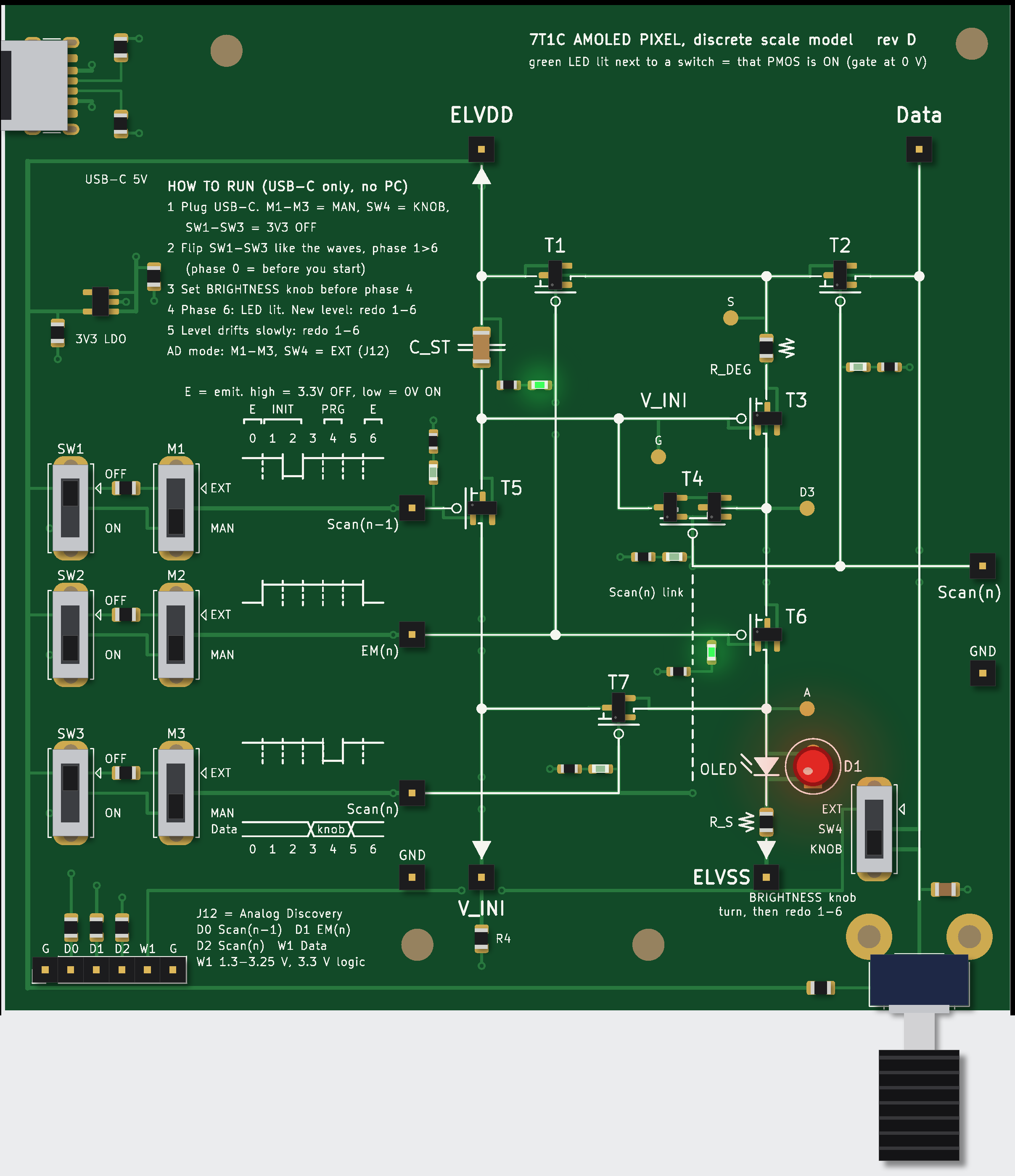
A green 0603 LED sits next to the gate of each switch transistor (T1, T2, T4, T5, T6, T7). It lights when that gate is at 0 V, i.e. when the PMOS is ON. Circuit: ELVDD -> 15 kOhm -> LED -> gate net, about 0.1 mA, so it adds no load in manual mode and under 0.15 V of gate lift when driven by the Analog Discovery.
Set M1-M3 = EXT and SW4 = EXT, then use J12:
| J12 pin | Signal | AD connection |
|---|---|---|
| 1, 6 | GND | GND |
| 2 | Scan(n-1) | DIO0 (0 V = ON, 3.3 V = OFF) |
| 3 | EM(n) | DIO1 |
| 4 | Scan(n) | DIO2 |
| 5 | Data | W1, DC 1.3-3.25 V (lower = brighter) |
Scope: CH1 across R_S gives LED current (10 mV per mA). CH2 on test point G (10x probe) shows the Vth-compensated gate sample. In EXT, each gate idles OFF through a 100 kOhm pull-up; 470 Ohm series resistors protect the DIO if a manual switch is also driving.
| Item | Value |
|---|---|
| Supply | USB-C 5 V (4.4-5.25 V) -> AP2112K -> 3.3 V |
| LED current | (3.3 V - Data) / 680 Ohm, about 0-1.9 mA, worst case about 2.3 mA |
| Transistors | Si2301CDS, Vth -0.4 to -1.0 V, max stress 3.3 V of 20 V |
| T4 | back-to-back pair (common source) so its body diode cannot leak C_ST |
| Path | Contents |
|---|---|
kicad/ | KiCad 7+ board (.kicad_pcb, .kicad_pro) |
fab/gerbers.zip | Gerbers + drill, upload to JLCPCB / PCBWay |
fab/BOM.csv, fab/pick_and_place.csv | Parts with MPNs, placement |
fab/drc_report.txt | KiCad DRC: 0 errors, 0 unconnected (only USB connector silk past edge) |
scripts/ | build.py + ctrl.py regenerate the whole board with KiCad's pcbnew Python API |
scripts/.Pixel topology: the standard 7T1C AMOLED compensation pixel from the open literature. Design by Bo (borenw).
| Qty | Value | Footprint | References |
|---|---|---|---|
| 10 | pin | PinHeader_1x01_P2.54mm_Vertical | J1, J2, J3, J4, J5, J6, J7, J8, J9, J10 |
| 8 | Si2301CDS | SOT-23 | T1, T2, T3, T4A, T4B, T5, T6, T7 |
| 7 | OS102011MS2QN1 | SW_Slide_SPDT_Straight_CK_OS102011MS2Q | M1, M2, M3, SW1, SW2, SW3, SW4 |
| 6 | 15k | R_0603_1608Metric | RL1, RL2, RL4, RL5, RL6, RL7 |
| 6 | LTST-C191KGKT | LED_0603_1608Metric | DL1, DL2, DL4, DL5, DL6, DL7 |
| 4 | M3 | MountingHole_3.2mm_M3 | H1, H2, H3, H4 |
| 4 | TP | TestPoint_Pad_D1.5mm | TP1, TP2, TP3, TP4 |
| 3 | 100k | R_0805_2012Metric | RP1, RP2, RP3 |
| 3 | 470R | R_0805_2012Metric | RS1, RS2, RS3 |
| 2 | 5.1k | R_0805_2012Metric | R5, R6 |
| 1 | 0R | R_0805_2012Metric | R4 |
| 1 | 100nF | C_0805_2012Metric | C3 |
| 1 | 10R | R_0805_2012Metric | R2 |
| 1 | 10k lin | Potentiometer_Bourns_PTV09A-2_Single_Horizontal | RV1 |
| 1 | 10nF C0G | C_1206_3216Metric | C1 |
| 1 | 1uF | R_0805_2012Metric | C5 |
| 1 | 240R | R_0805_2012Metric | R7 |
| 1 | 4.7uF | R_0805_2012Metric | C4 |
| 1 | 6.8k | R_0805_2012Metric | R8 |
| 1 | 680R | R_0805_2012Metric | R1 |
| 1 | AD port | PinHeader_1x06_P2.54mm_Vertical | J12 |
| 1 | AP2112K-3.3 | SOT-23-5 | U2 |
| 1 | USB4125-GF-A | USB_C_Receptacle_GCT_USB4125-xx-x_6P_TopMnt_Horizontal | J11 |
| 1 | WP710A10LID | LED_D3.0mm | D1 |

uw-roamr/roamr
turn your phone into a robot running SLAM with two motors, two control boards, and a bluetooth chip

Lucas-Poulos/uwb-rescue-locator
The fixed reference station. Open bay-station.kicadpro in KiCad.

r4hulrr/ausign
Real-time Auslan (Australian Sign Language) to English speech translation glove. Built with ESP32-S3, flex sensors, IMU on a custom PCB, and a Bluetooth-connected Python GUI.

juleswwebb/portfolio
A static engineering portfolio for https://juleswwebb.github.io/portfolio/.

ginomcfino/auv-sensor-hub
STM32-based sensor hub for autonomous underwater vehicles, integrating CAN bus communication, inertial and pressure sensing, and multi-rail power regulation.

jpconstantineau/NRF52-Board
This Repository is a collection of NRF5x boards.

It measures 100 × 100 mm and has 2 copper layers, 1.6 mm thick.
67 parts, built around the AP2112K-3.3, SI2301CDS, OS102011MS2QN1 and LTST-C191KGKT. The full list of its parts is on this page, with links to each part's symbol and footprint where PCBKit's library has them.
From the borenw/oled-7t1c-pixel-pcb repository on GitHub, at the commit this page was made from: the board is kicad/oled_7t1c_pixel.kicad_pcb. PCBKit opens the board in the browser, with nothing to install.
Its repository states no licence, so its author keeps all rights: ask borenw before reusing the design.