

2 layers254 × 43.2 mm
NODE DATAPAC 256K historical reproduction
bkw777/NODE_DATAPAC
Reproduction & documentation of Node Systems DATAPAC
25 parts7

 bkw777/NODE_DATAPAC7
Reproduction & documentation of Node Systems DATAPAC
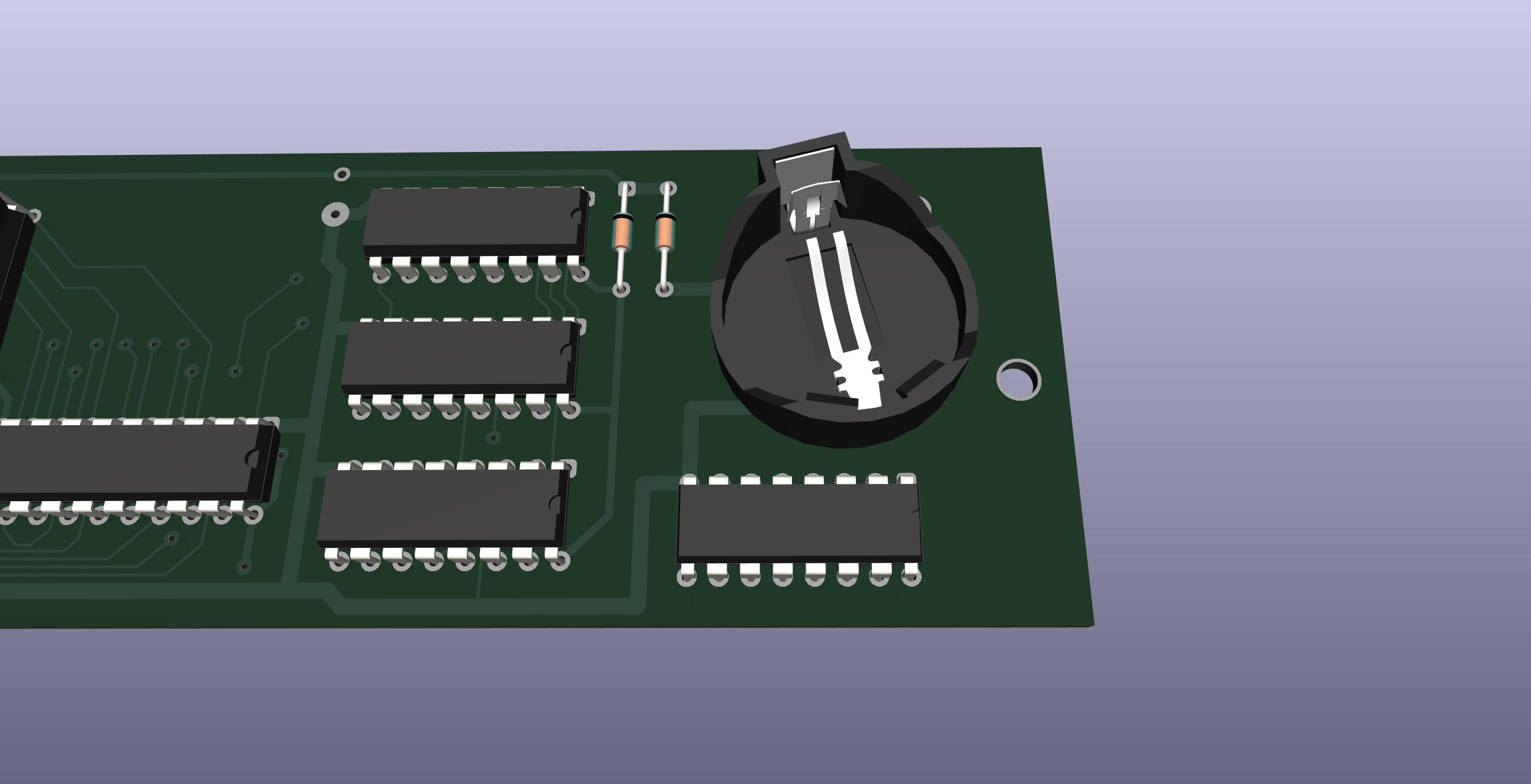
NODE DATAPAC 256K bkw is an open-source printed circuit board by bkw777, from the bkw777/NODE_DATAPAC repository on GitHub. It is a 2-layer board of 255.3 × 43.2 mm with 31 parts on 76 nets, routed with 729 tracks and 161 vias.
It is built around the HC138 and CR2032. Its parts include 10 ICs, 7 capacitors, 3 diodes, 2 resistors and 1 connector.
This repo documents the NODE Systems DATAPAC, rampac, and a new clone, the MiniNDP.
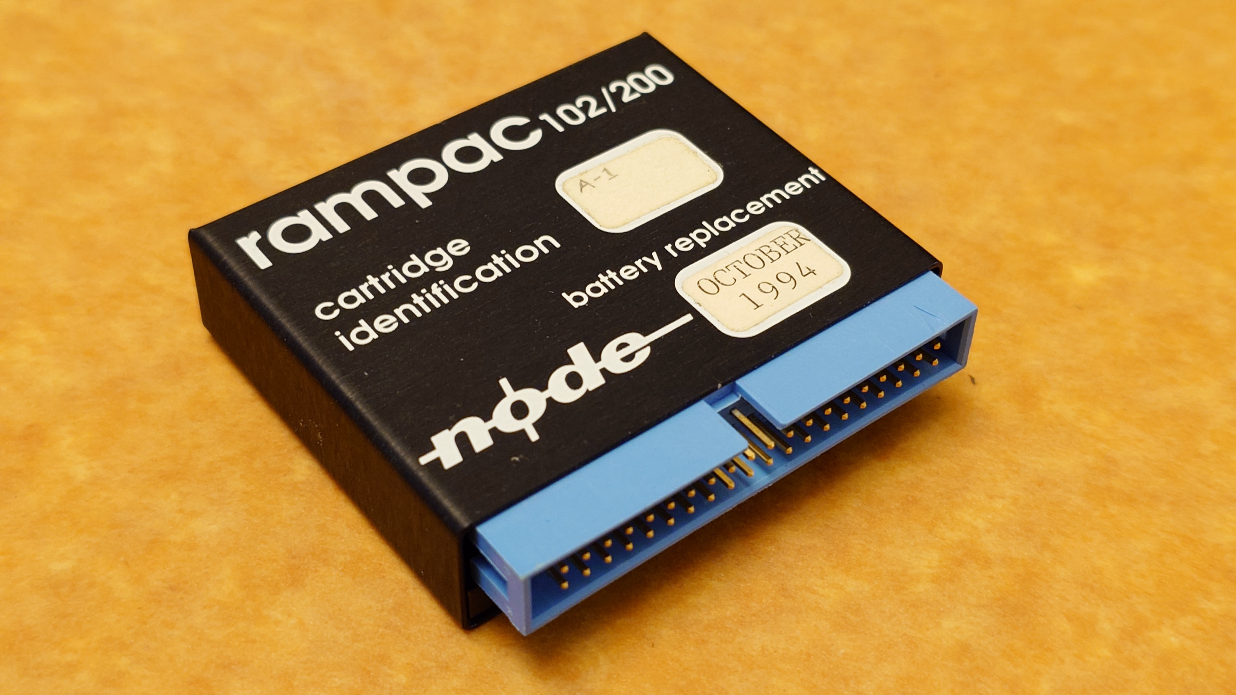
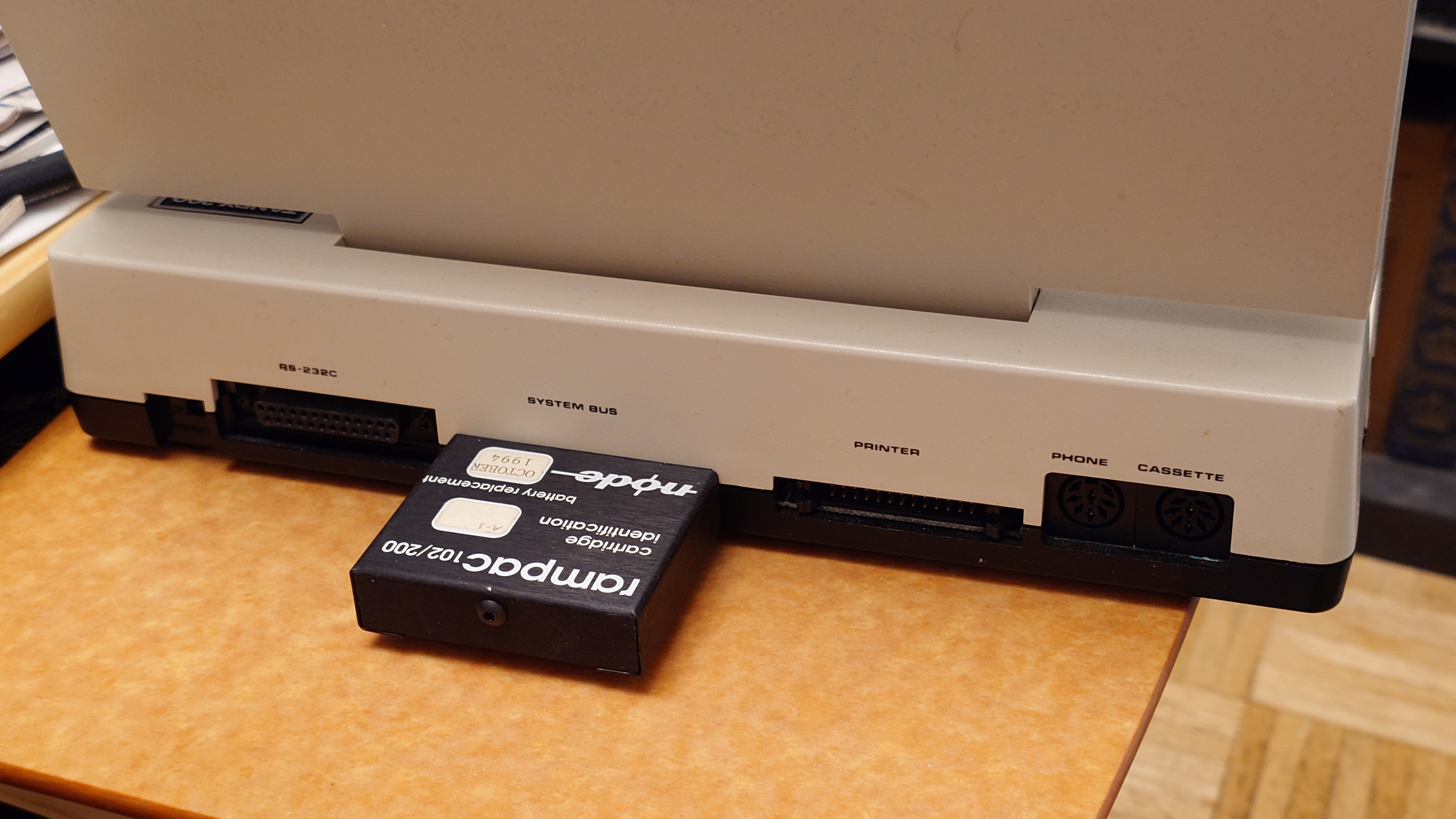
The NODE Systems DATAPAC/rampac was a popular ram disk peripheral for TRS-80 / TANDY Models 100, 102, & 200 computers.
The schematic and PCB below documents the DATAPAC.
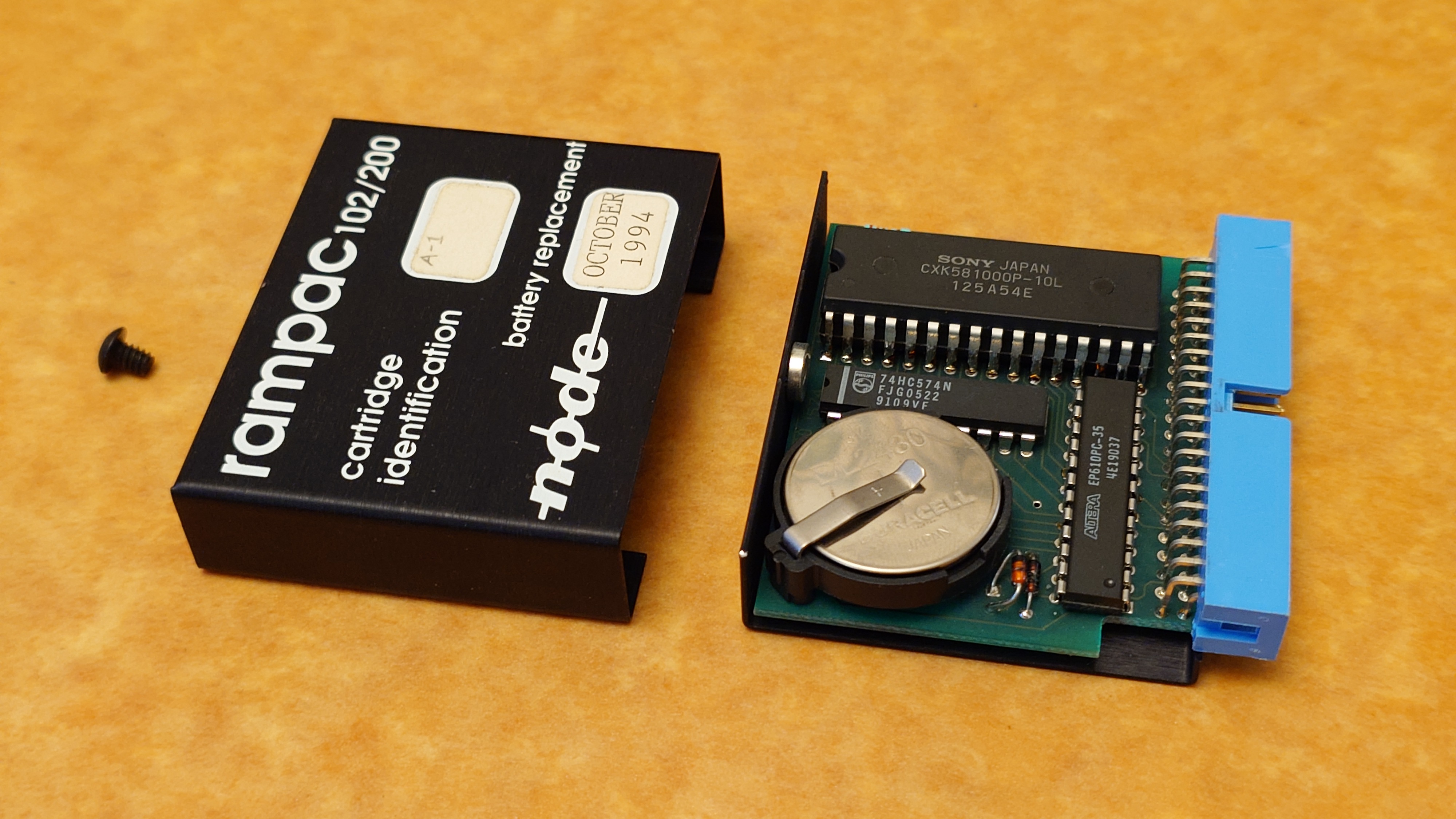
rampac is a smaller later version of the same device that uses fewer larger sram chips and replaces most of the discrete logic IC's with a single PLD, but functions exactly the same.
Here is some disorganized INFO mostly gathered from the M100SIG archive and club100.
TLDR: To use the hardware, install RAMDSK, and what you get is a ram disk of 128k to 1M depending on model and installed ram.
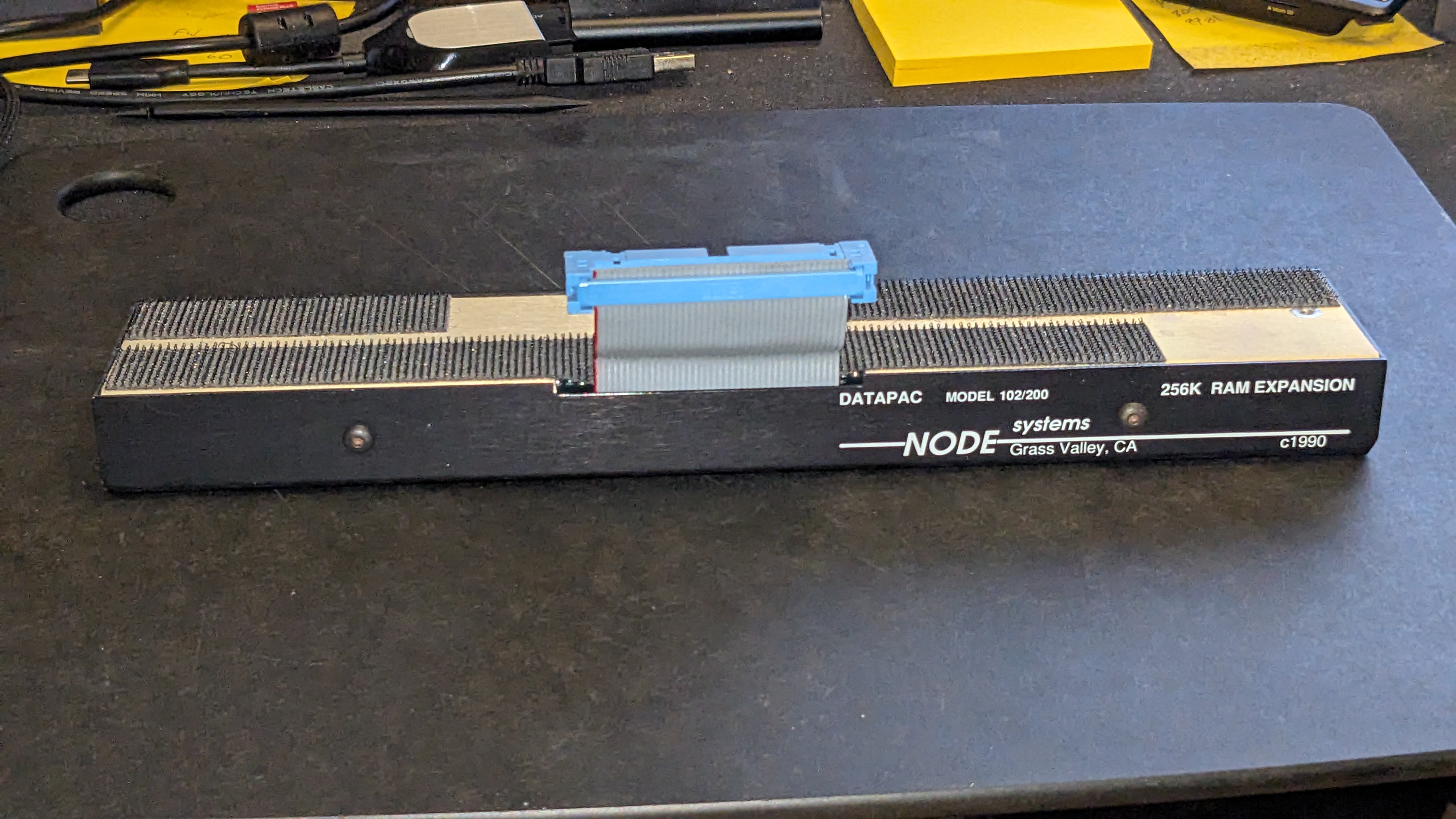
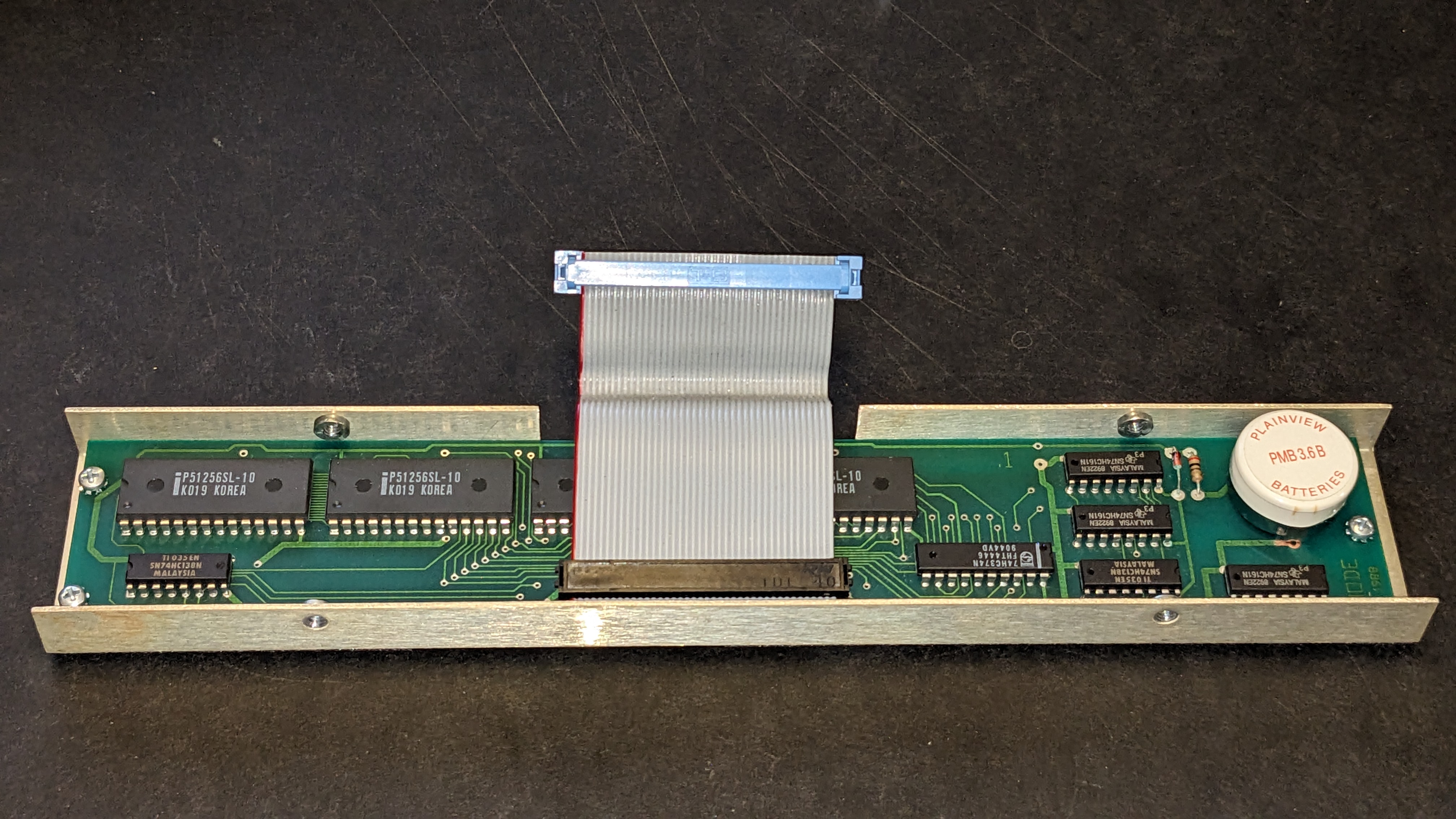
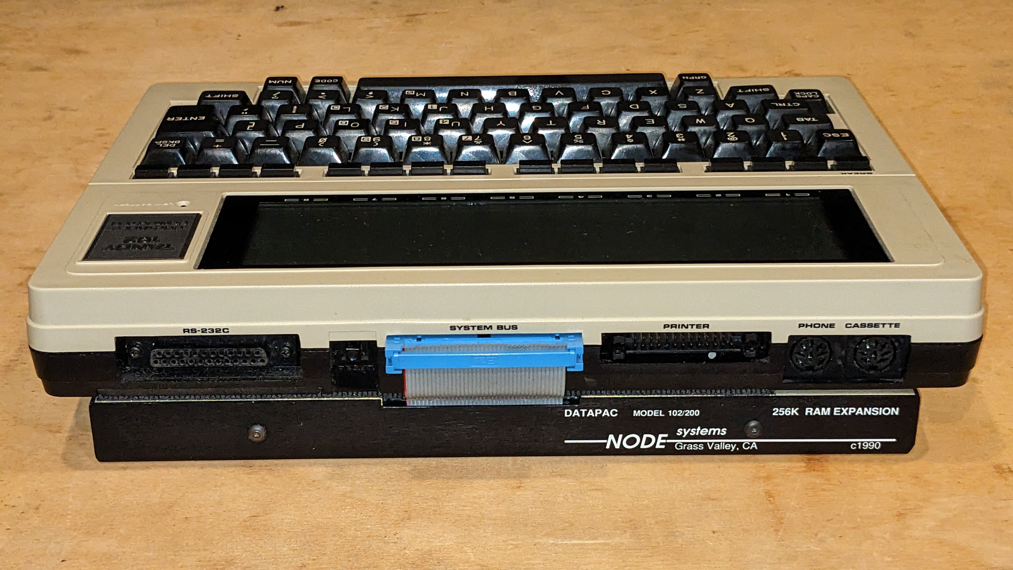
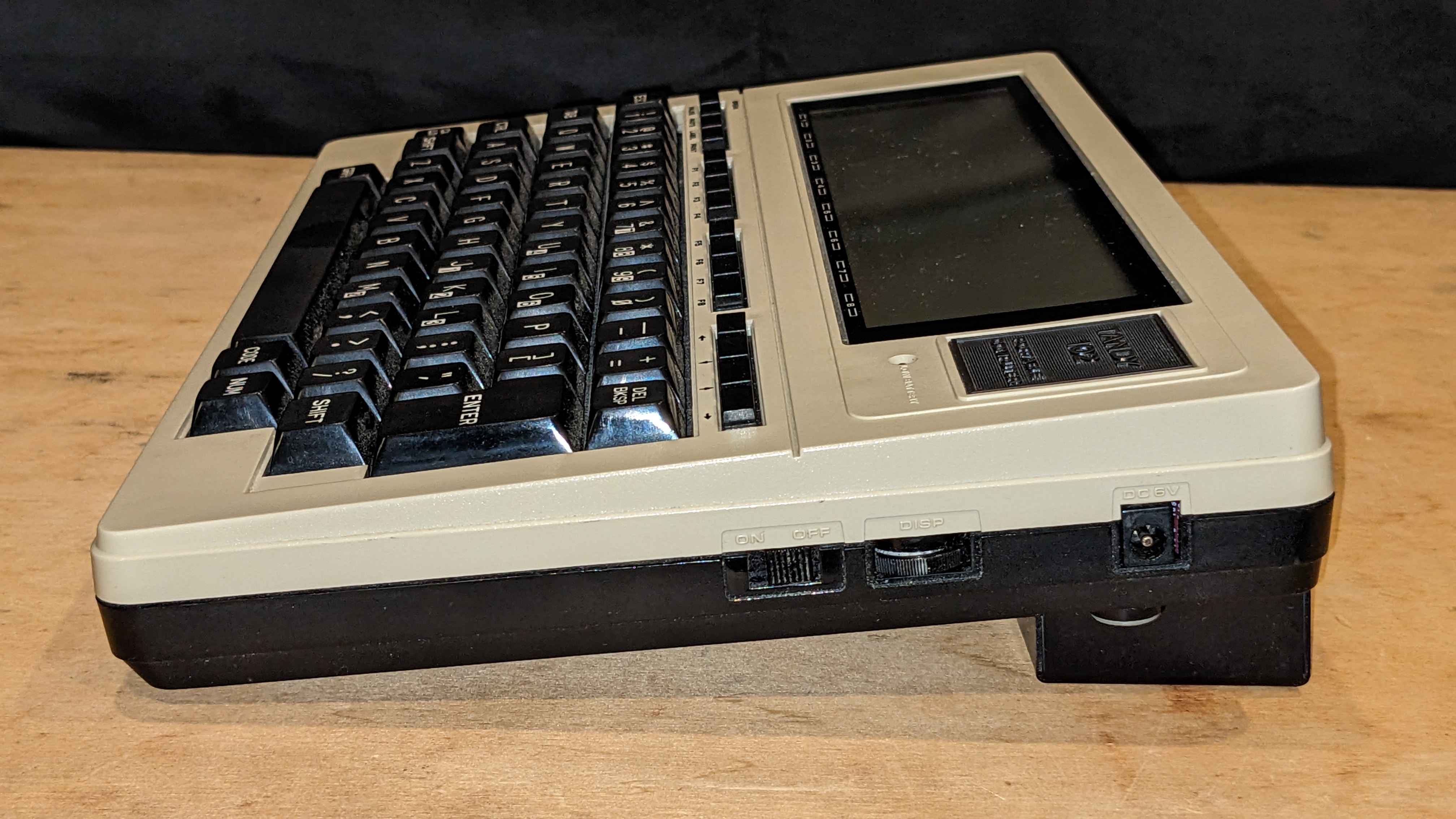
The original text file manual RAMDSK.DO.
The NODE ROM that came with the unit generates this file when formatting a device.
There are also some discussions in the M100SIG archive and Paul Globmans software on club100.
Most of these are collected in docs.
See also the docs for the various bits of software.
Other References
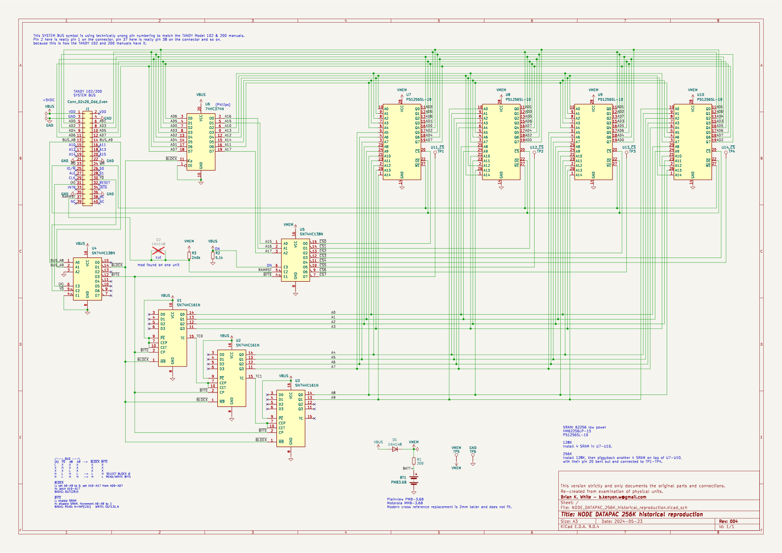
This is a new drawing but aims to reflect the original actual device as exactly as possible.
It's meant to be a form of documentation or reference describing the original hardware as it was.
For instance, the ungrounded inputs on the 161's, the inconsistent thickness of power traces, the fact that only 1 of the 2 bus VDD pins is connected, the VCC trace that almost touches one of the mounting screw heads, etc, are all exactly as in the original.
(I added a fiber washer to that screw in my units after noticing that. The case is not connected to ground, but still...)
For a historical reproduction version of the original PCB (minus the NODE copyright mark), see: NODE_DATAPAC_256K_historical_reproduction.kicad_pro
For a version of the original PCB that still uses the same components and fits in the same case, but cleans up a few things, see: NODE_DATAPAC_256K_bkw.kicad_pro
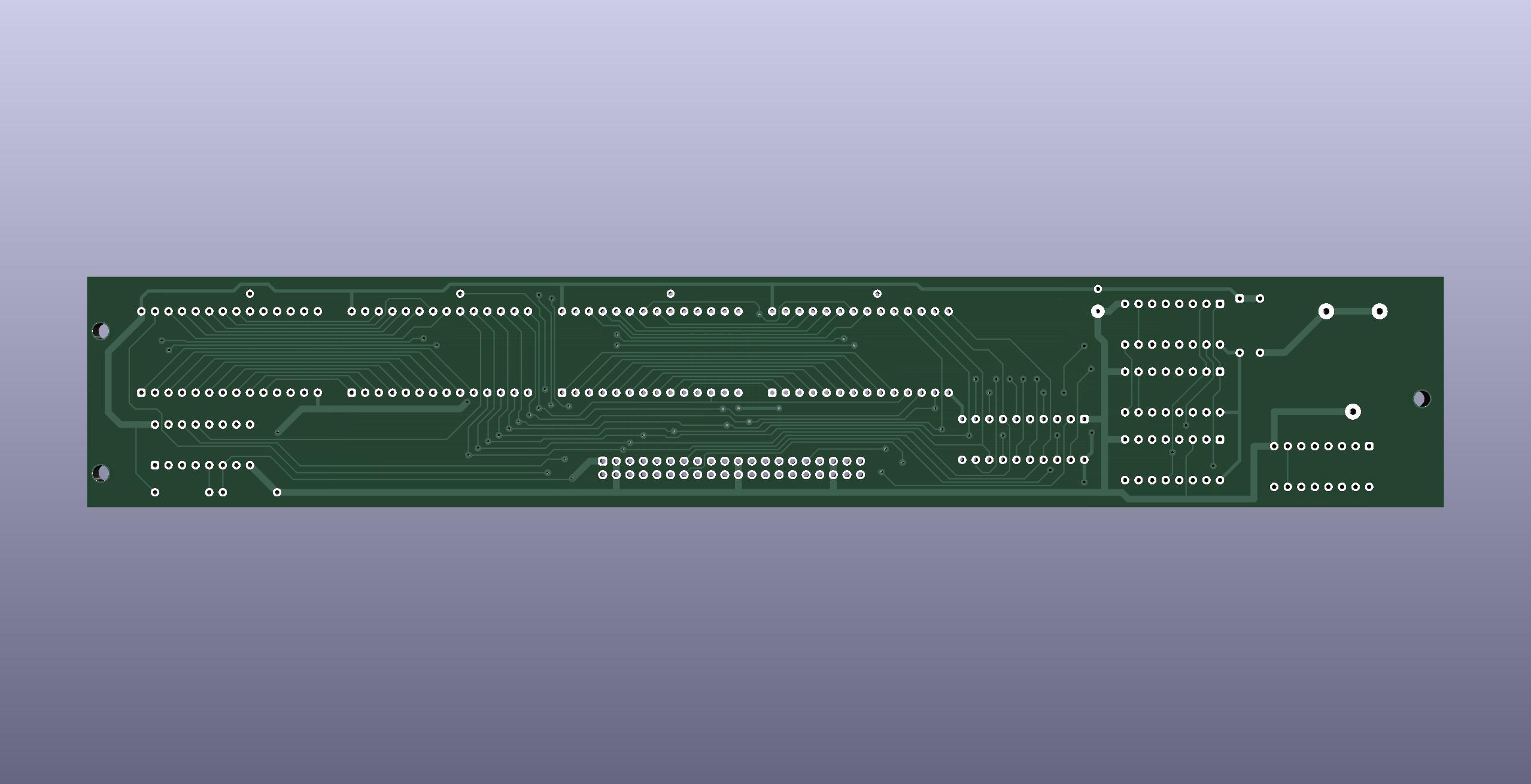
PCB TOP
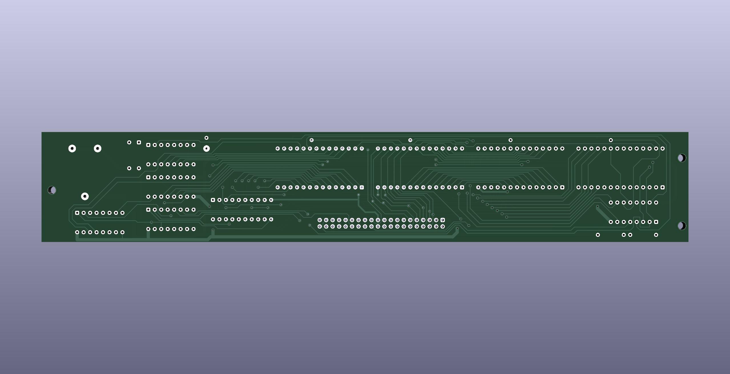
PCB BOTTOM
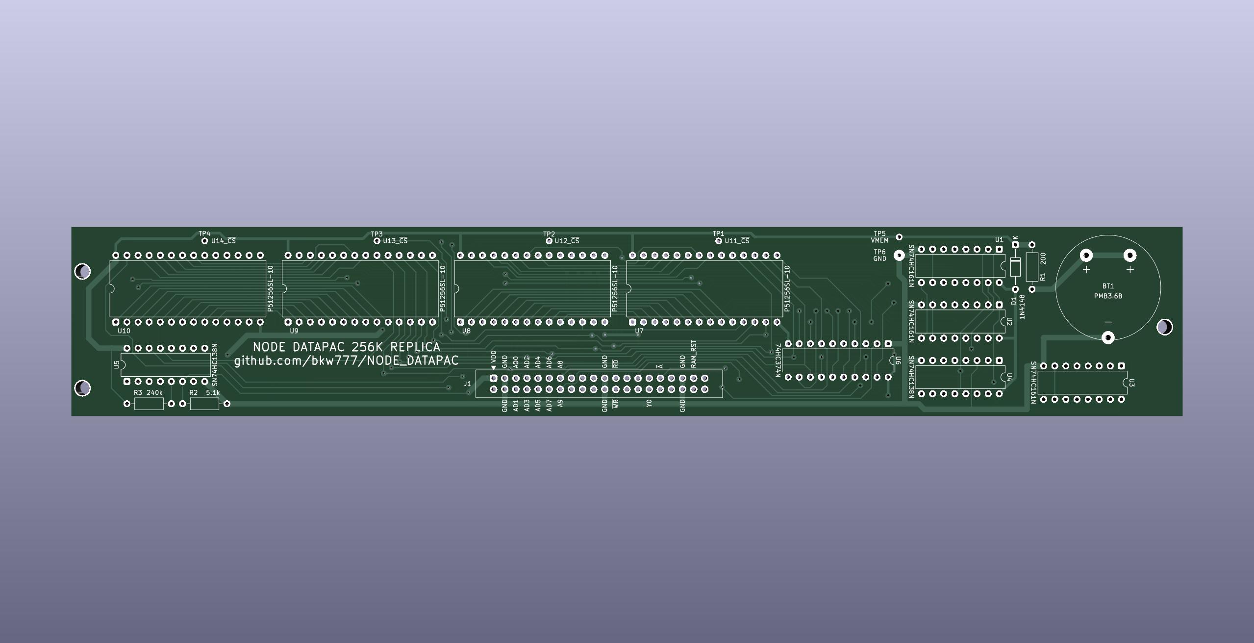
The original PCB has no silkscreen. This image has silkscreen added to show where the components from the schematic go.
The circuit has 2 functions, SELECT-BLOCK and READ/WRITE-BYTE, controlled by the internal active-low signals /BLOCK and /BYTE.
The U4 HC138 monitors four lines from the bus, /Y0 (A) A8 A9, and based on that asserts either /BLOCK or /BYTE or neither.
If neither /BLOCK nor /BYTE is asserted then the bus traffic has no effect on any of the other chips.
The 3 HC161 form a 0-1023 counter, setting SRAM address bits A0-A9.
Call this the byte-number or byte-position counter or offset.
The HC374 sets SRAM address bits A10-A17 from the bus data bits AD0-AD7, and latches that value on its outputs until triggered to update to a new value.
Call this the block-number or block selector.
The U5 HC138 converts 3 bits of the block-number into 1 of 8 chip-select to select 1 of 8 32K SRAM chips,
and also monitors both /BYTE and RAMRST and disables all ram while either /BYTE or RAMRST is high.
When /BLOCK goes low:
When /BLOCK goes high:
When /BYTE goes low:
When /BYTE goes high:
The byte-number and block-number combine to form the current address in SRAM at any given time.
The device provides up to 256 blocks (8-bit block-number) of 1024 bytes each (10-bit byte-number).
The host computer first does a SELECT-BLOCK to select a block number from 0-255, then does READ-BYTE or WRITE-BYTE to read or write one byte of data at byte number 0 in that block, then repeats the BYTE operation up to 1023 more times to read or write up to all 1024 bytes in the block.
If you read or write more than 1024 times without selecting a new block, the byte-number counter just rolls over to 0 again.
You can also mix reads and writes in the same block. Each read OR write advances the byte position the same way each time, regardless if the previous operation was a read or a write. For instance in order to skip over 64 bytes without modifying them and then start writing at the 65th byte, you would read-and-ignore 64 times and then start writing.
"ramdisk" is an appropriate term because the device actually does operate like a disk even though it has no brains or firmware. The block-select latch acts like a track or sector address, and the binary counter acts like a disk or tape head reading or writing a sequential stream of bytes.
Later versions of RAMPAC were offered with 384k or 512k by adding a second bank of up to 256k, and later versions of RAMDSK.CO know how to access the 2nd bank.
In 512K units, the extra 256K is accessed by the state of bus address line A10 during a SELECT-BLOCK operation.
SELECT-BLOCK with BUS_A10 low accesses bank0, with BUS_A10 high accesses bank1.
All other aspects are the same, so accessing bank0 on a a 512K device is the same as accessing the only bank on a 256K device. Old software is still compatible with bank0 on new hardware, new software is still compatible with old hardware.
What this all means from the host computer software side of things
The original battery is no longer made, and the modern cross-reference is almost 2mm taller and does not fit inside the enclosure.
NODE Systems themselves used to perform an update to older units to replace the original rechargeable NiCD cell with a non-rechargeable lithium cell which was supposed to last about 5 years.
The change is simple and easy, and the parts are common. You just remove the old battery and the 200 ohm resistor, and replace them with a CR2032 holder and a diode. That's it. Both parts fit and solder right in the same locations where the old parts came out. Point the diode stripe away from the battery, just like the other diode that is right there next to it. Any standard diode will do. Schottky is not recommended because the reverse leakage is not good for a lithium cell. Another 1N4148 like the one that's already there is perfect.
This should give at least 4 years of memory.
(The original NiCD battery may have only lasted as little as a few months per charge according to a review in the archives. So the coin cell mod is not merely more conveniently available with current parts, it's an improvement.)
BEFORE
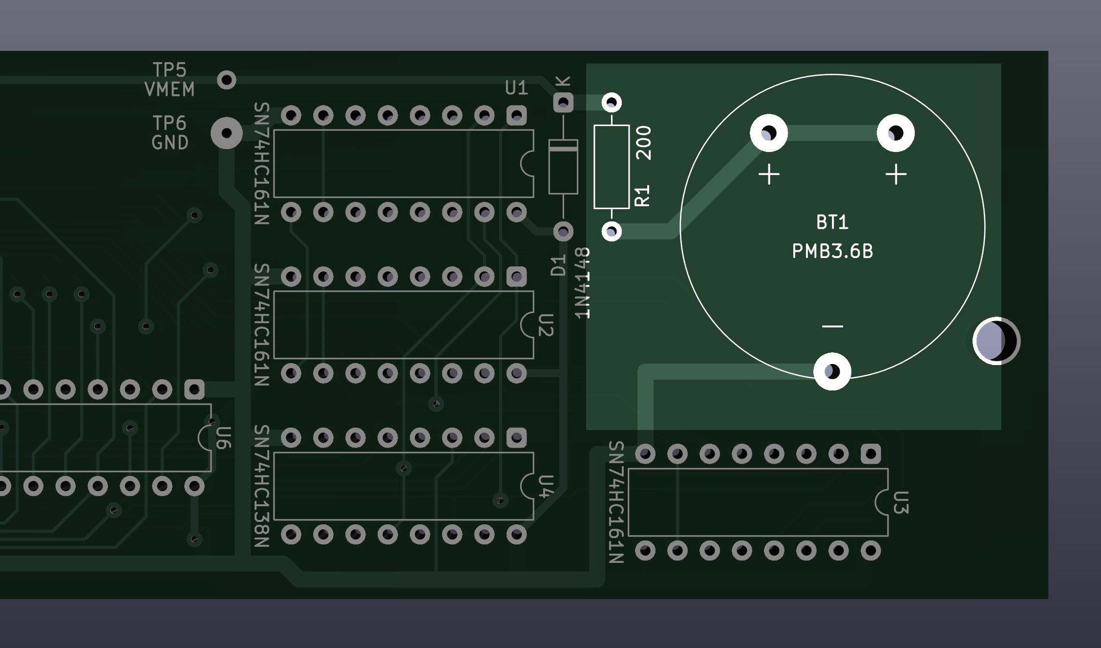
AFTER
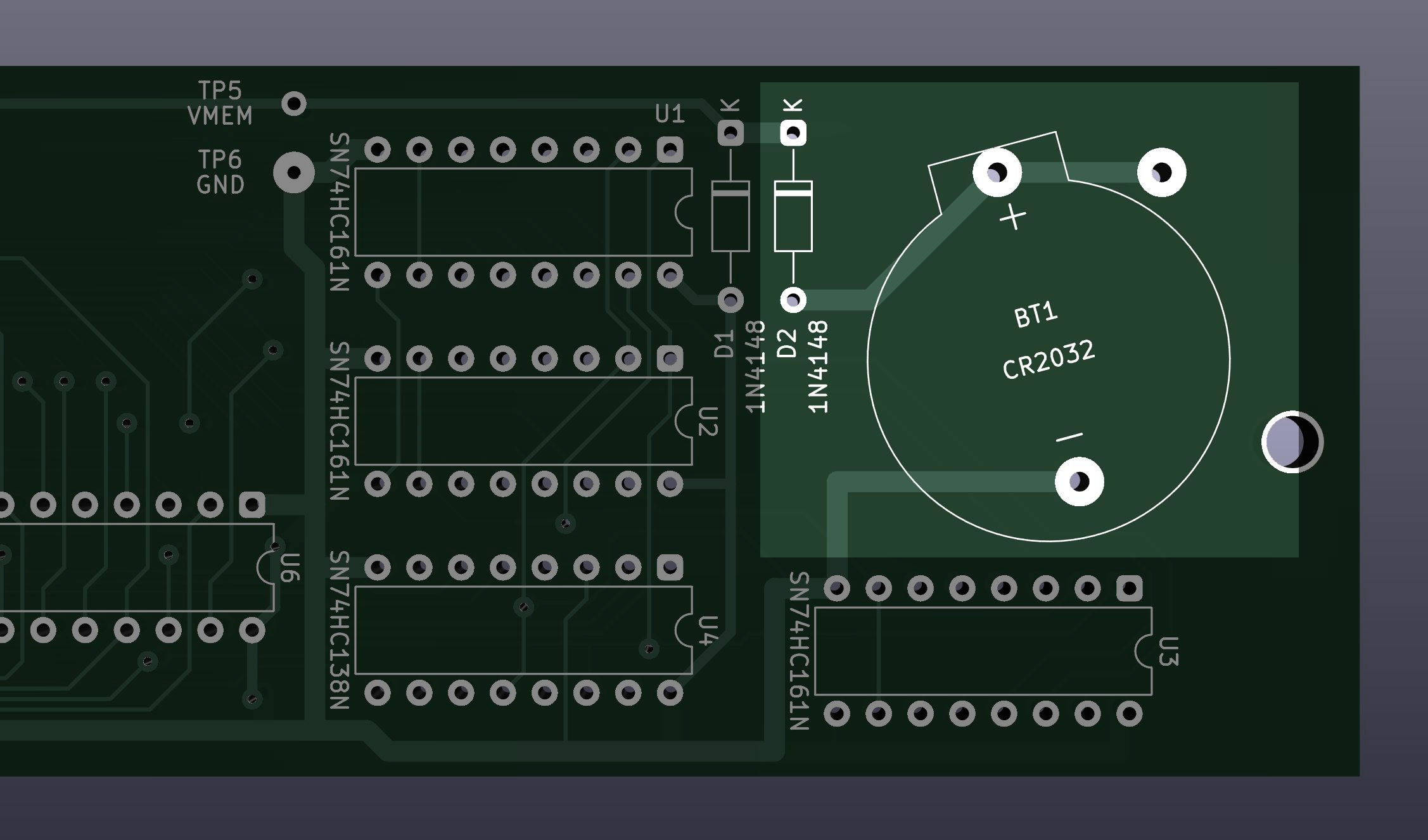
STEPS
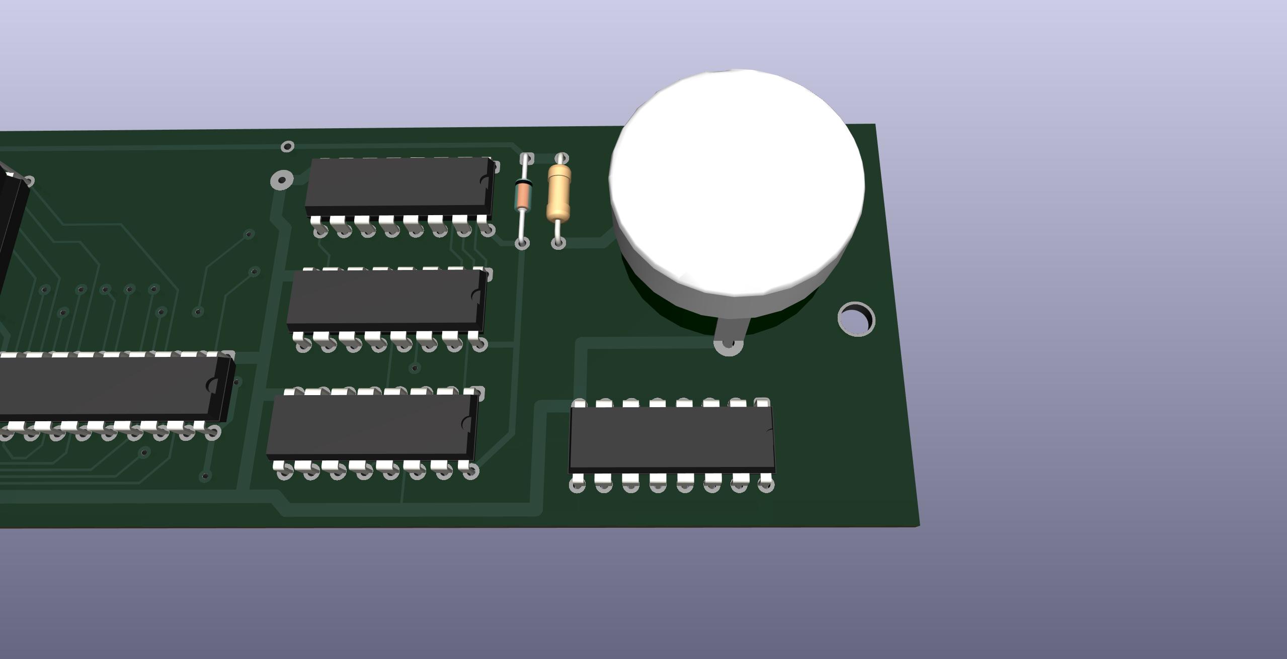
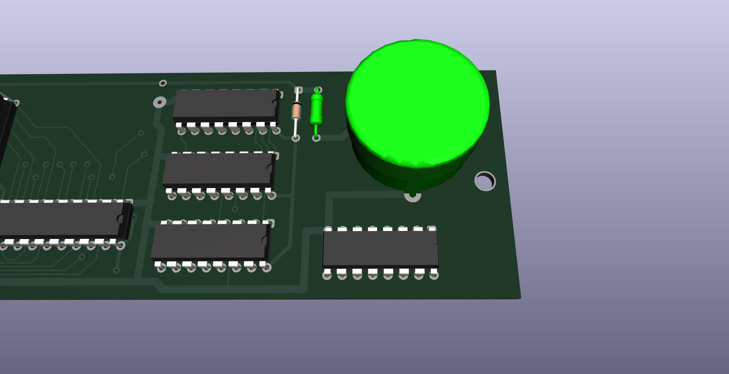
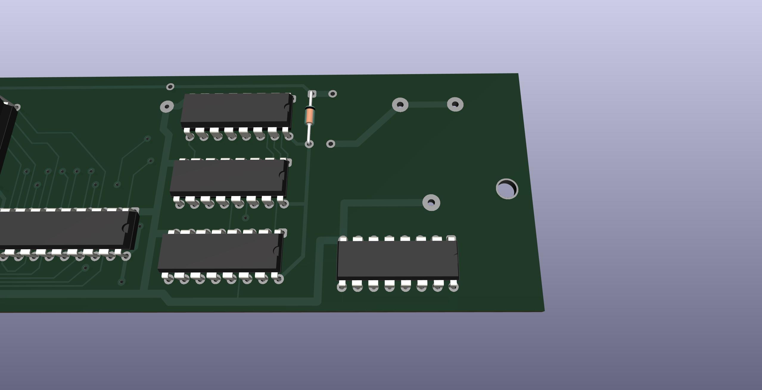
If you wish to keep using a rechargeable battery, then one suitable option is FL3/V80H. That is 3 16x5.8mm NiMH button cells in a flat in-line pack with wire leads. It fits perfectly in the space next to the ribbon cable. It needs to be secured with hot glue or foam mounting tape, and connected with wires run to the original battery location.

The charging circuit is utterly basic, so do not connect any other type of battery except NiCD or NiMH.
You can use any cell form factor and any larger or smaller mAh capacity, but must be 3.6v and only NiCD or NiMH chemistry.
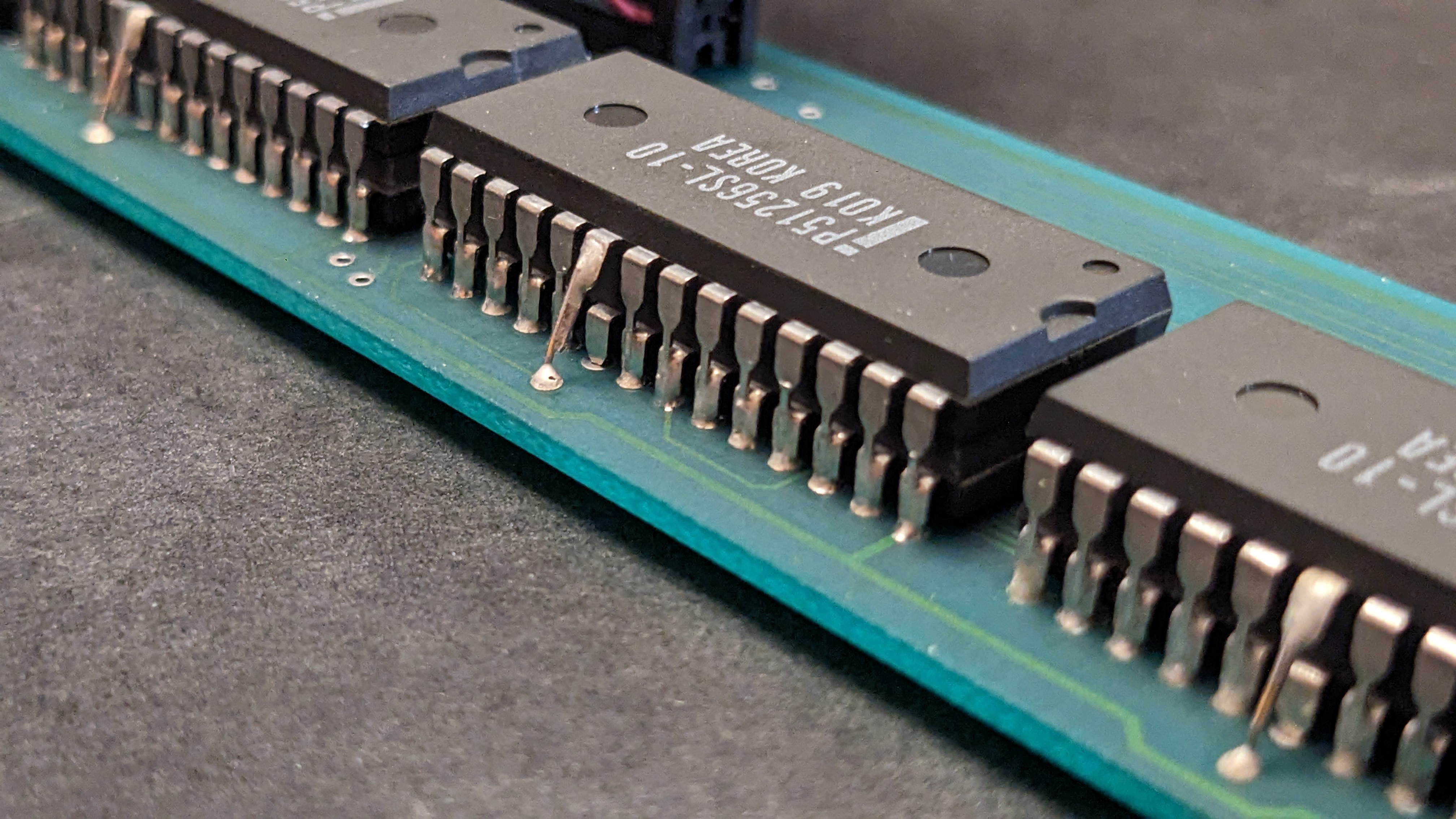
A 128k unit may be upgraded to 256k by just adding 4 more SRAM chips piggy-backed onto the existing chips.
The PCB has 4 DIP-28 footprints for the SRAM chips.
Each DIP-28 footprint also has an extra via close to pin 20.
A 128k unit has a low-power 62256 installed in each footprint, and nothing connected to the via near pin 20.
To get 256k, a second set of chips are soldered piggyback on top of the first four.
All pins except pin 20 (chip-select) are simply soldered to the chip below.
Pin 20 is bent out and connected to the extra via on the pcb (with a short bit of wire to reach) and not connected to the chip below.
No other parts or changes are needed to upgrade an existing 128k unit to 256k.
Any 62256 will work, but for old parts you want the low-power version for standby battery life.
New parts already naturally have as low or lower standby current than the low-power versions of old parts even if they don't say "low power".
Old standard: HM62256 70uA
Old lowpower: HM62256LP 4uA
Old lowpower: P51256SL 2uA
New standard: AS6C62256 1uA
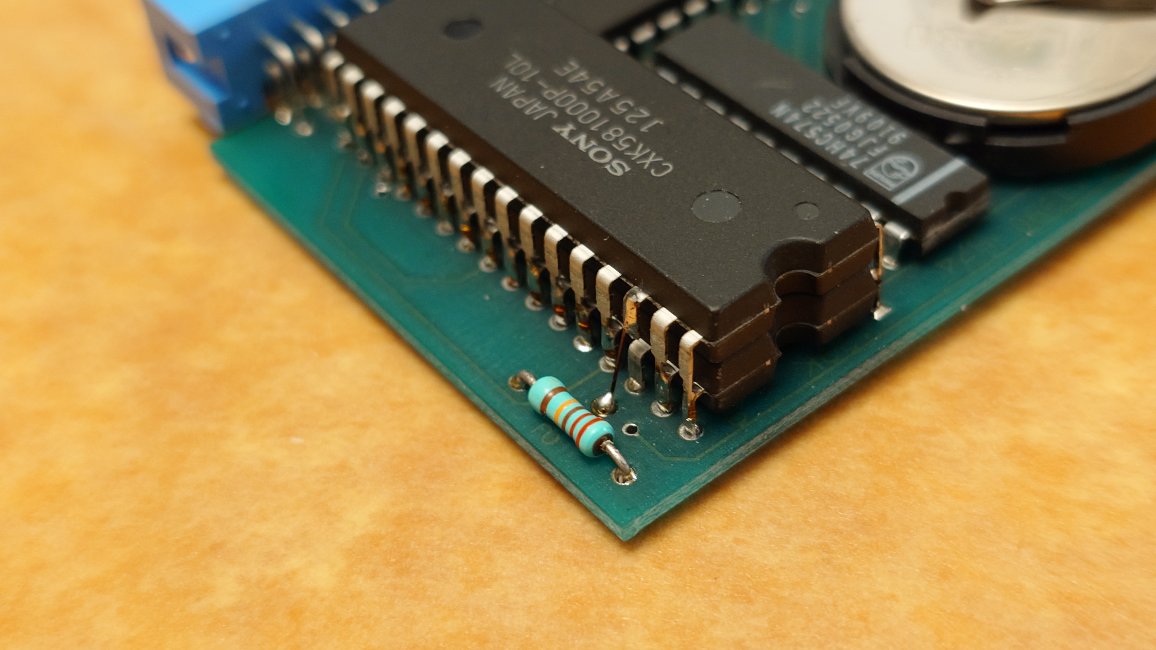
The same is true for rampac. Except:
Originally only North-American Models 100, 102, & 200 were ever supported.
Kyotronic KC-85 and Olivetti M-10 are also supported today because RAMDSK has been disassembled and ported, and the assembly source means the international models could be added as well.
The device is not compatible with NEC PC-8201/PC-8300.
Although the DATAPAC was primarily designed for Model 102 & 200, the crimp-on boxed male IDC pin header on the cable does not actually fit into a 200 without enlarging the opening around the bus connector on the 200. If you want to connect an original DATAPAC to a 200 without hacking up the 200's case or modifying the DATAPAC cable, you can build a small adapter by just soldering a male & female solder-type 2x20 boxed pin headers back to back. The solder box header does fit in the opening.


The DATAPAC case says "102/200", but it also works on Model 100, K85, and M10 with the right adapter cable. It's electrically compatible with everything but NEC.
For 100 & K85 the cable is just an IDC-DIP-40 aka "DIP-40 wire-to-board" connector and a standard 2x20 female IDC connector, both crimped onto a 40-pin ribbon cable about 8 inches long.
The Model 100 adapter part of this 3-part Disk/Video Interface Cable is the same thing.
For Olivetti M-10 the cable is even simpler, a standard female to female IDC 40-pin ribbon cable.
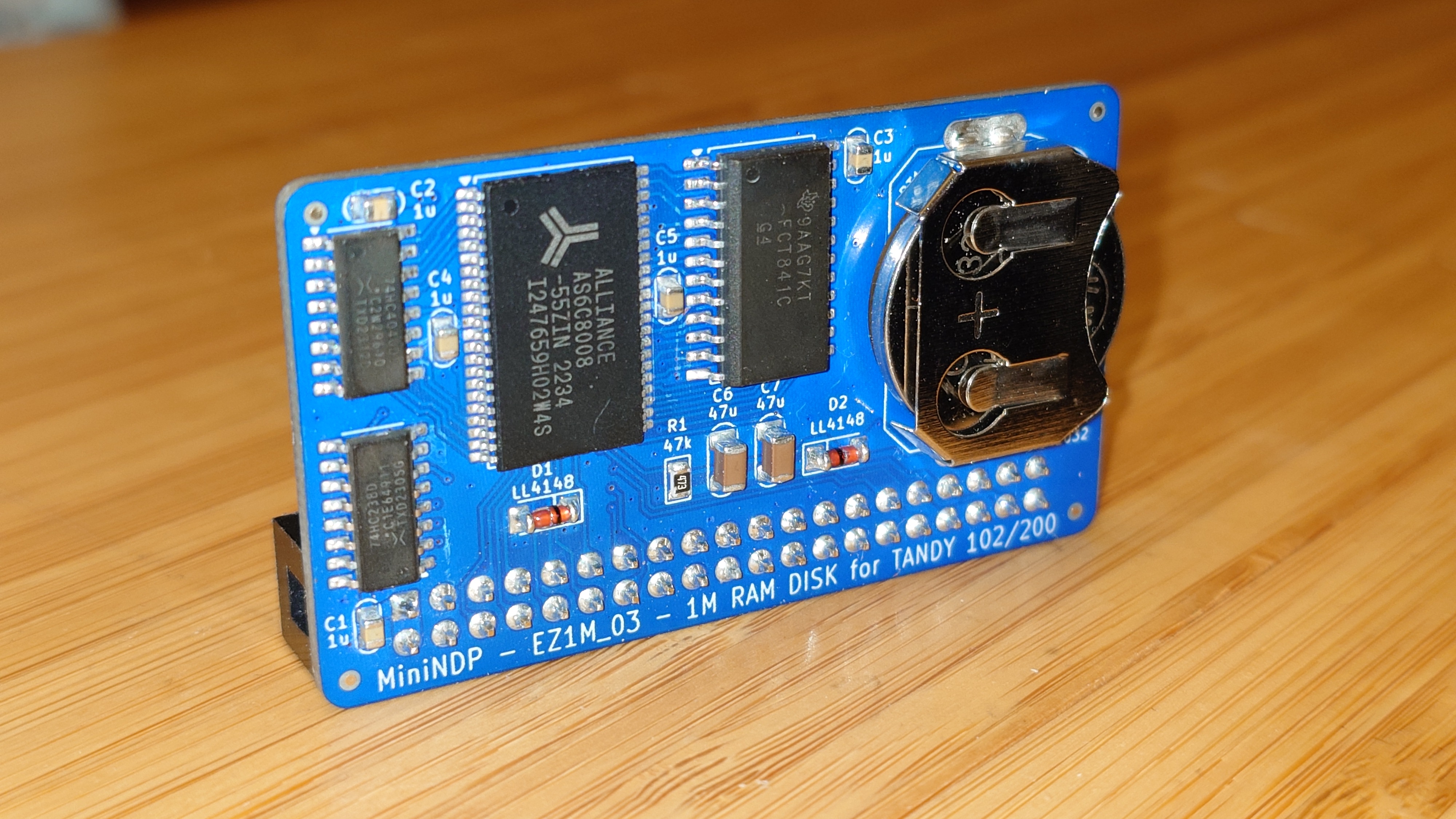
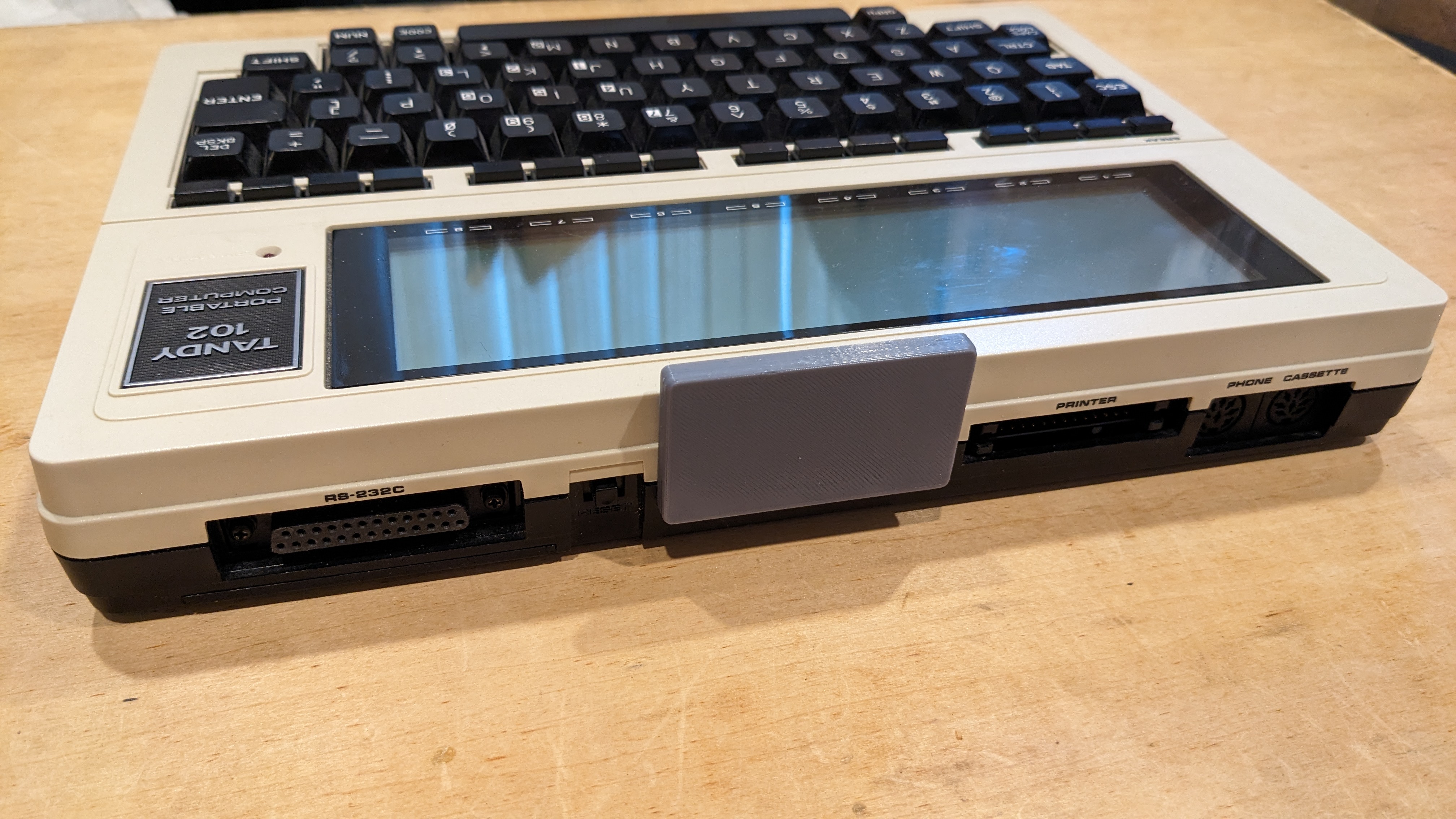
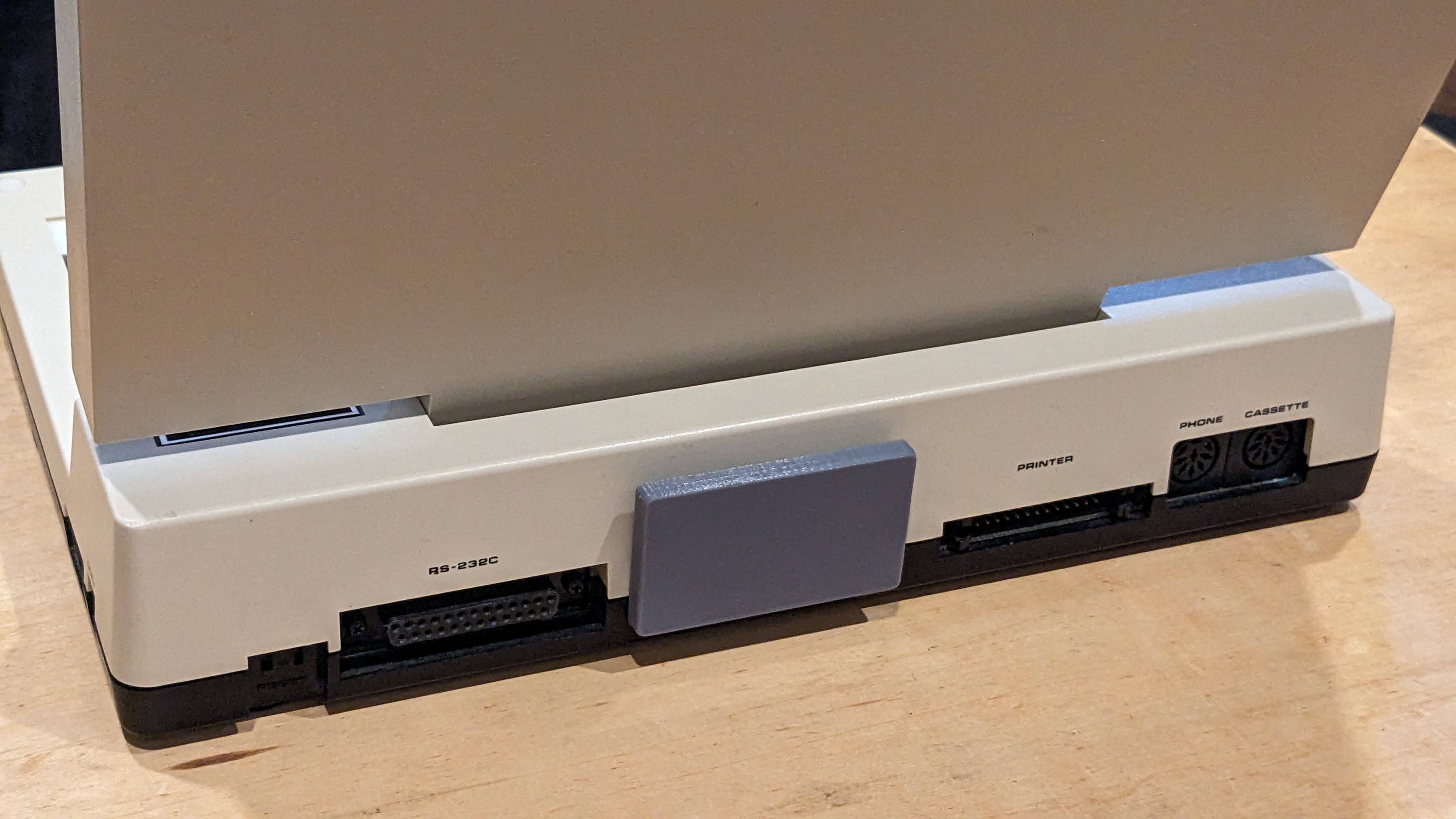
MiniNDP fits directly on both 102 and 200 with no adapter or cable, or M10 with a female-female ribbon cable at least 5 inches long.
MiniNDP_u1M fits directly in the bus socket of 100 or K85 with no adapter or cable, and the cover can even be closed over it.
Originally these shipped with an OPTION ROM from NODE called RAMDISK.
Later, Paul Globman wrote RAMDSK.CO, and that was eventually licensed by NODE and shipped with new units.
Later still, RAMDSK was updated with 2 changes:
Recently, RAMDSK has been updated yet further:
Some other software culled from the M100SIG archive and Club100 are collected here in the software directory.
How to access the hardware from BASIC.
See RAMDSK.DO for the NODE ROM routines.
See RAMDSK.TIP for the RAM100.CO/RAM200.CO routines.
But note, the addresses in RAMDSK.TIP are incorrect for RAMDSK v2. We don't have a copy of RAMDSK v1 for 100 but we do for 200. So you can't follow those directions exactly except with RAMDSK v1 on 200.
The latest RAMDSK built from the new source includes *.calls files that give the current addresses to the routines in those binaries, but actually using them has not been tested.
There are two low level operations that you use to access the device,
BLOCK and BYTE, and each of those has two variations, for four total ops.
Select a BLOCK from BANK 0
OUT 129,n
Selects block# n (0-255) in bank 0, and resets the byte position to 0.
Select a BLOCK from BANK 1
OUT 133,n
Selects block# n (0-255) in bank 1, and resets the byte position to 0.
Read a BYTE
INP(131)
Reads the byte at the current byte position, and advances the byte position by one.
Write a BYTE
OUT 131,n
Writes the value n (0-255) to the current byte position, and advances the byte position by one.
The first read or write after selecting a block# applies to byte #0 of that block.
The byte position advances by one after each read or write, so the next read or write will be byte #1, then byte #2, etc up to 1024.
If you read or write more than 1024 times without selecting some other block, the byte position just rolls over to 0 again.
The position counter advances the same whether reading or writing.
Since the device can only read or write a single unsigned byte at a time, it's most efficient to use integer variables.
Use the % suffix or DEFINT: B%=INP(131) or DEFINT B : B=INP(131)
The general sequence is always:
1 - select a bank+block
2 - read/write byte 0-1024 times
To seek to an arbitrary offset before reading or writing, read-and-ignore that many bytes.
For instance, in RBOOT.DO, to skip over the first 16 bytes of the block, it does FORA=0TO15:N=INP(131):NEXT
N is not actually used, it's just reading 16 times and ignoring the data. This just advances the byte position counter to get from byte #0 past the 10-byte RAMDSK header and 6-byte .CO header to the start of the .CO executable data.
Examples
Select bank 0 block 0
OUT129,0
read a byte, which will be byte #0 of this block
INP(131)
Read and print the ascii of all the bytes in bank 0 block 2.
(this will mess up the display from control bytes if there is a binary .CO file in this block)
10 OUT 129,2
20 FOR I=0 TO 1023
30 PRINT CHR$(INP(131));
40 NEXT
Do the same but in bank 1
change line 10 to:
10 OUT 133,2
Manually repair the first two bytes of block 0 to mark the bank as being formatted without touching any of the data.
This means:
OUT129,0:OUT131,64:OUT131,4
(BTW you usually don't need to do this because RAMDSK.CO will do it for you.)
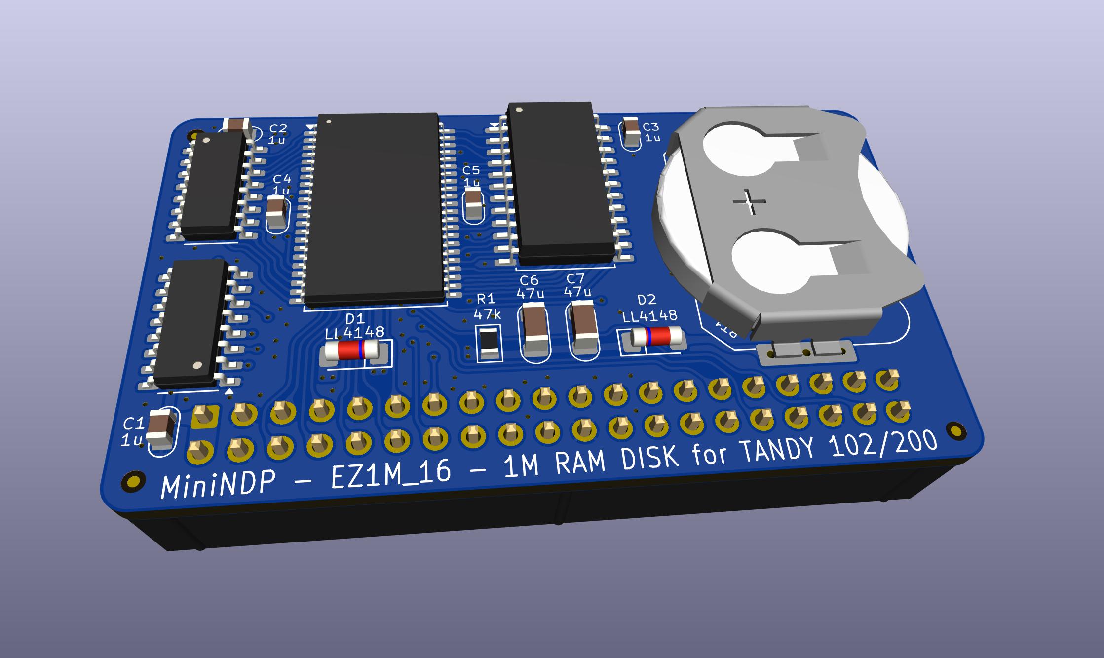
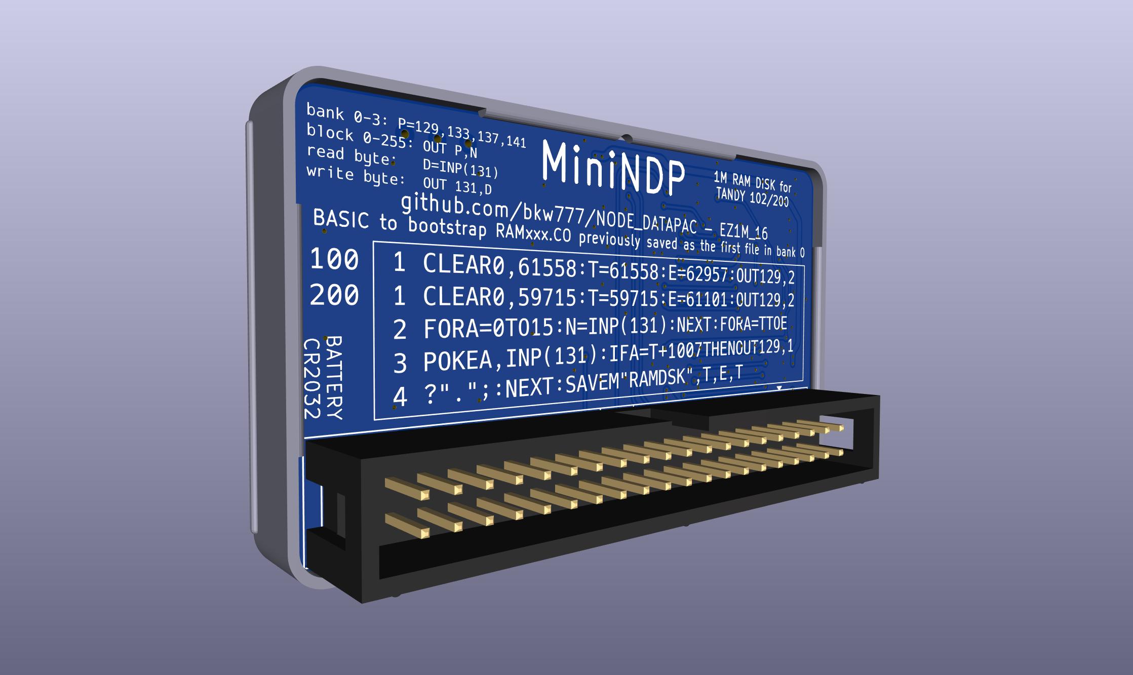
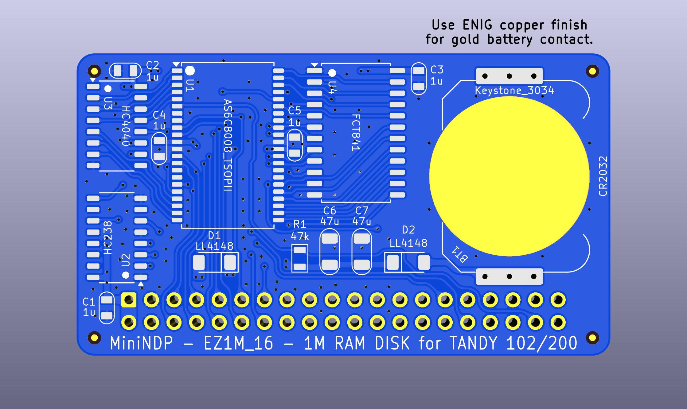
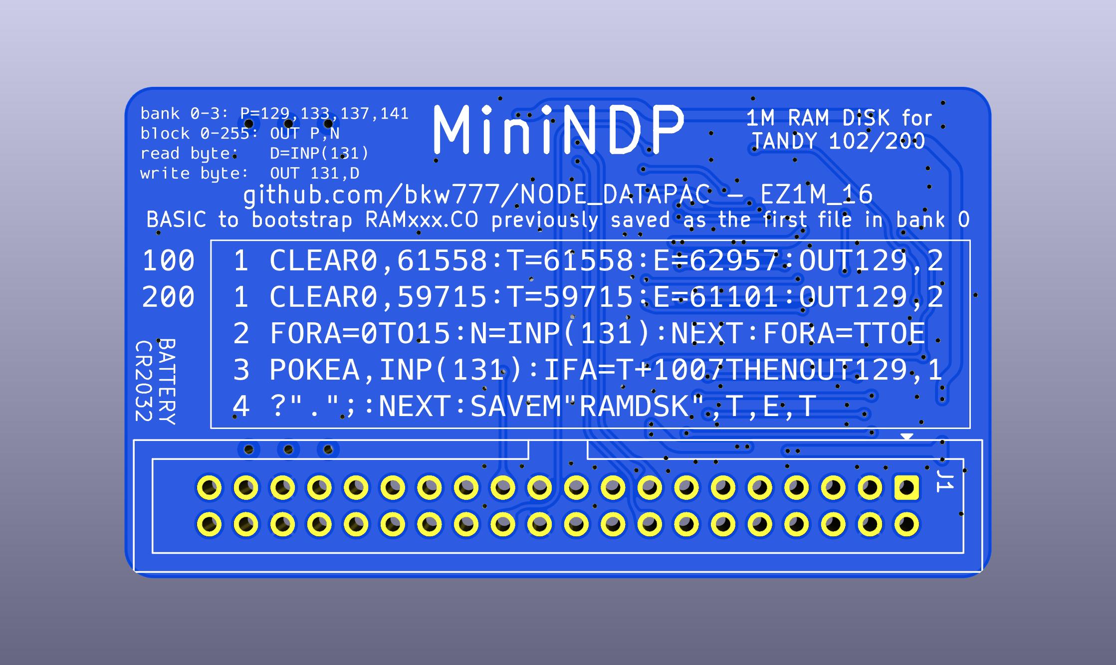
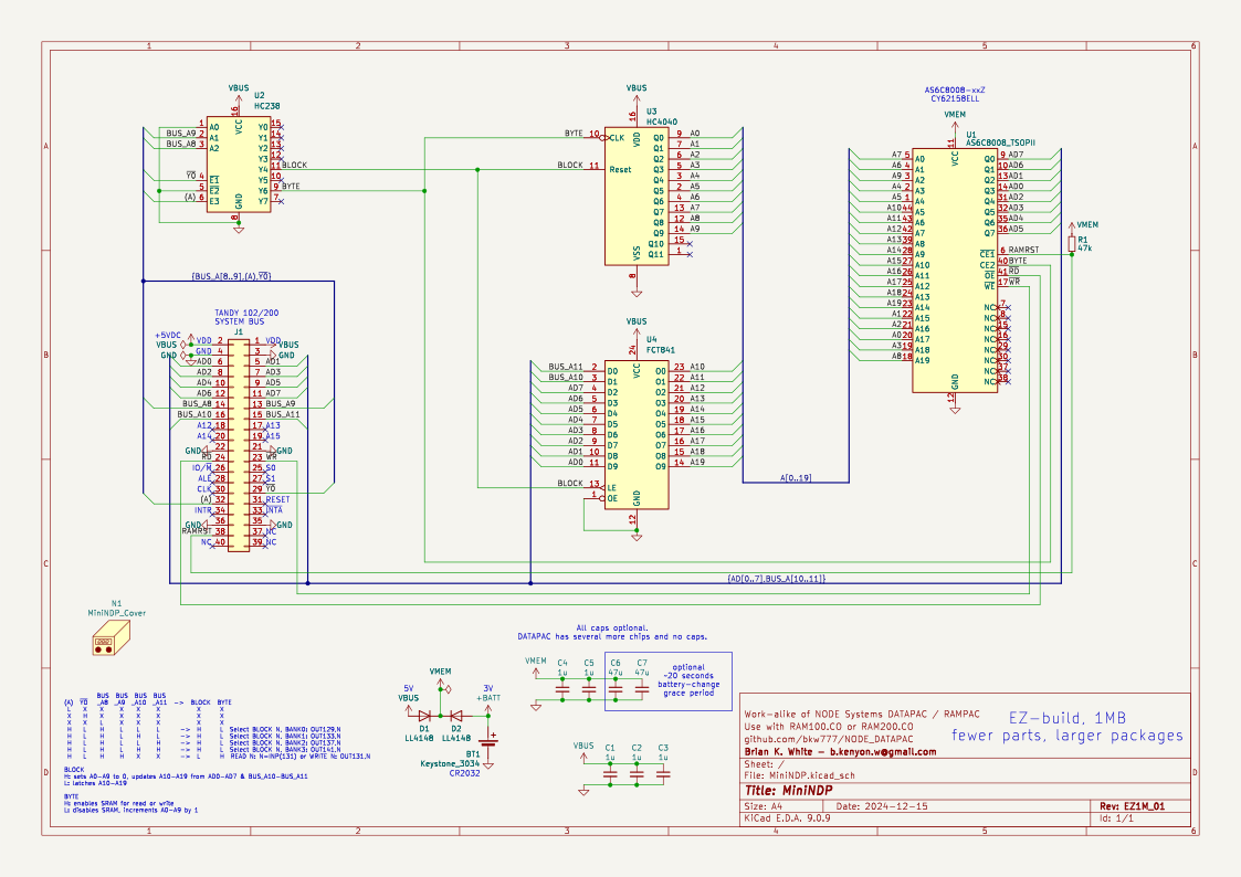
New design that functions the same as DATAPAC/rampac.
1 megabyte in 4 banks of 256k.
How to access all 4 banks:
Select bank 0, block N: OUT 129,N
Select bank 1, block N: OUT 133,N
Select bank 2, block N: OUT 137,N
Select bank 3, block N: OUT 141,N
Everything else works the same as normal DATAPAC/rampac.
Unlike the original DATAPAC, this actually fits into the bus port on the Model 200 without having to hack it's case.
BOM: DigiKey
MiniNDP EZ1M_16 PCB @ OSHPark
Cover: MiniNDP_Cover.stl -- Cover @ JawsTec
Both PCB & Cover @ PCBWAY
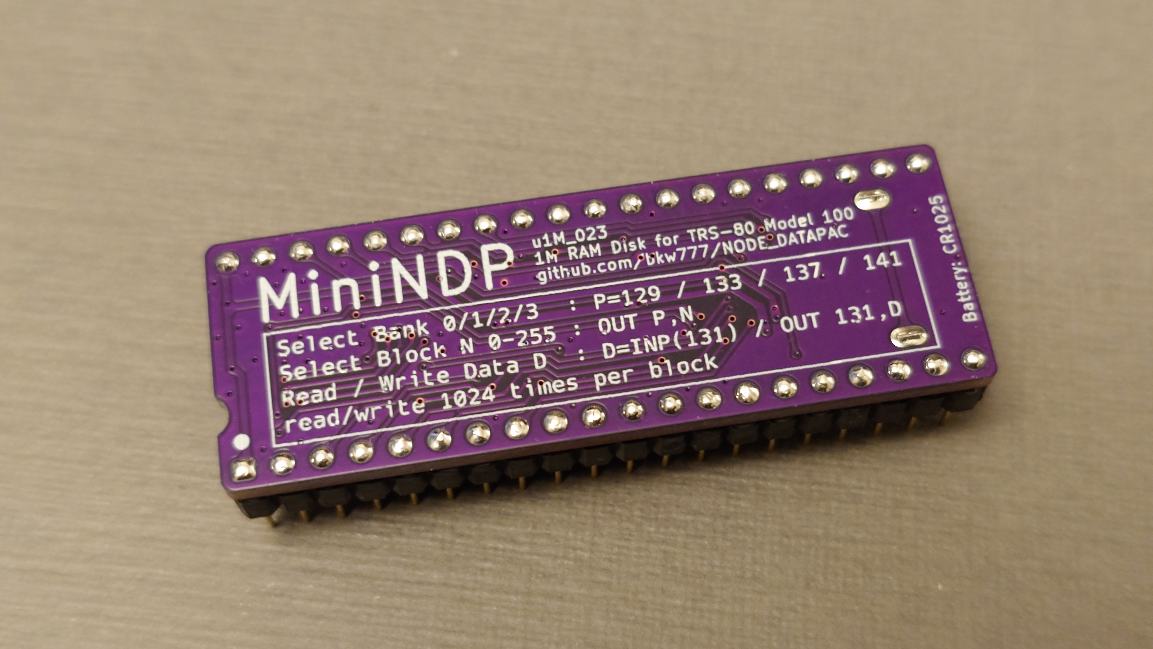
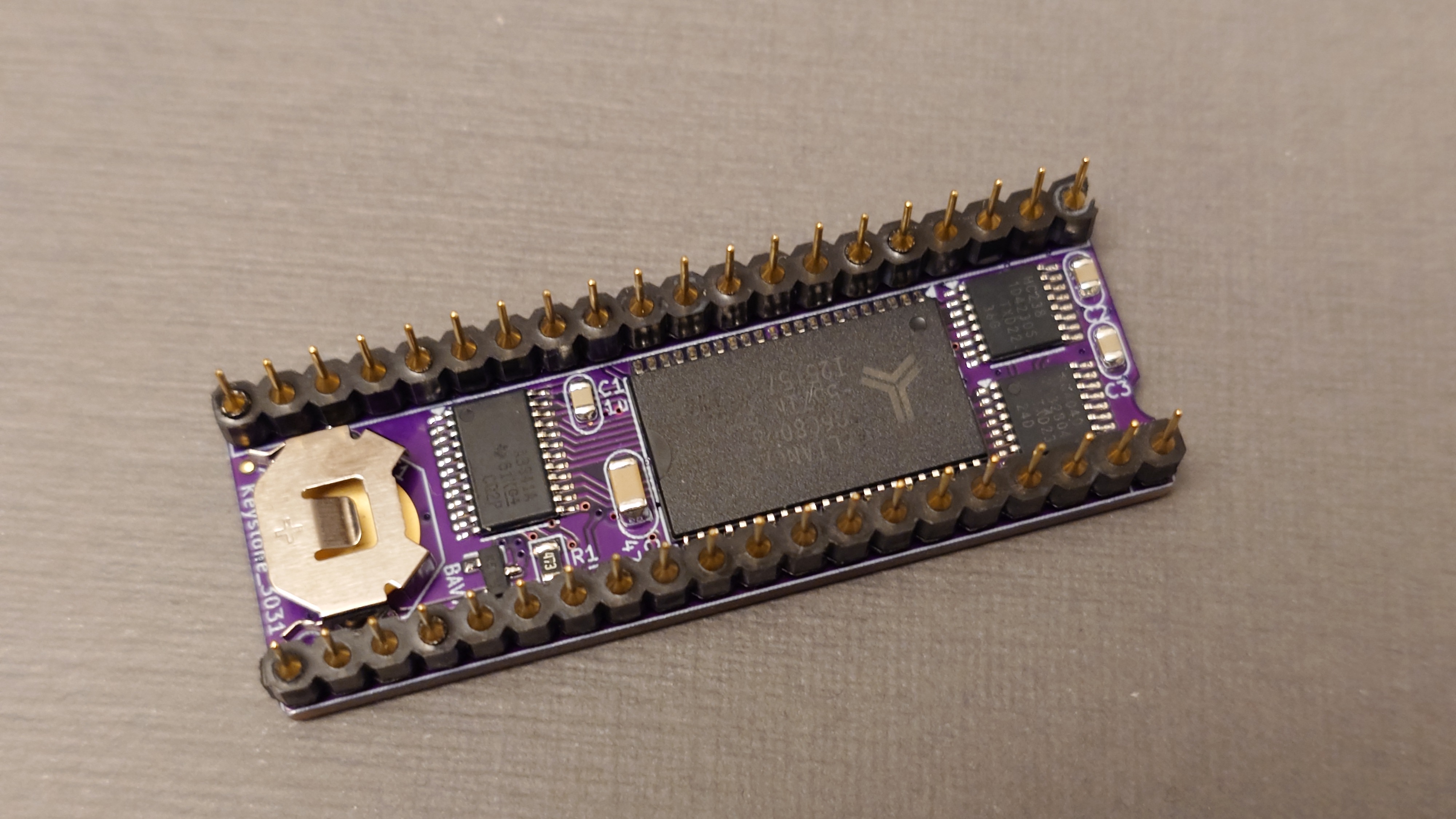
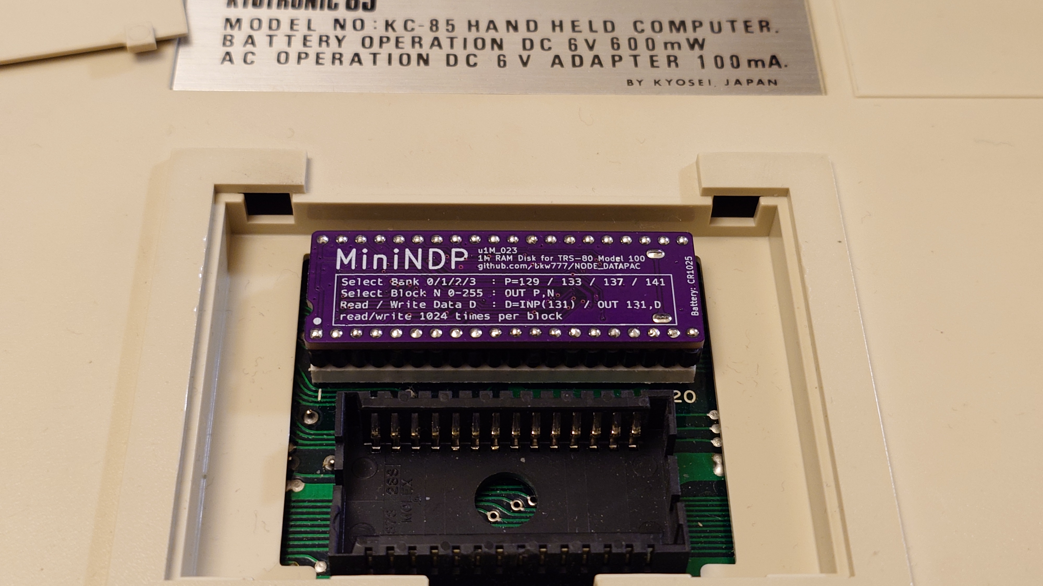
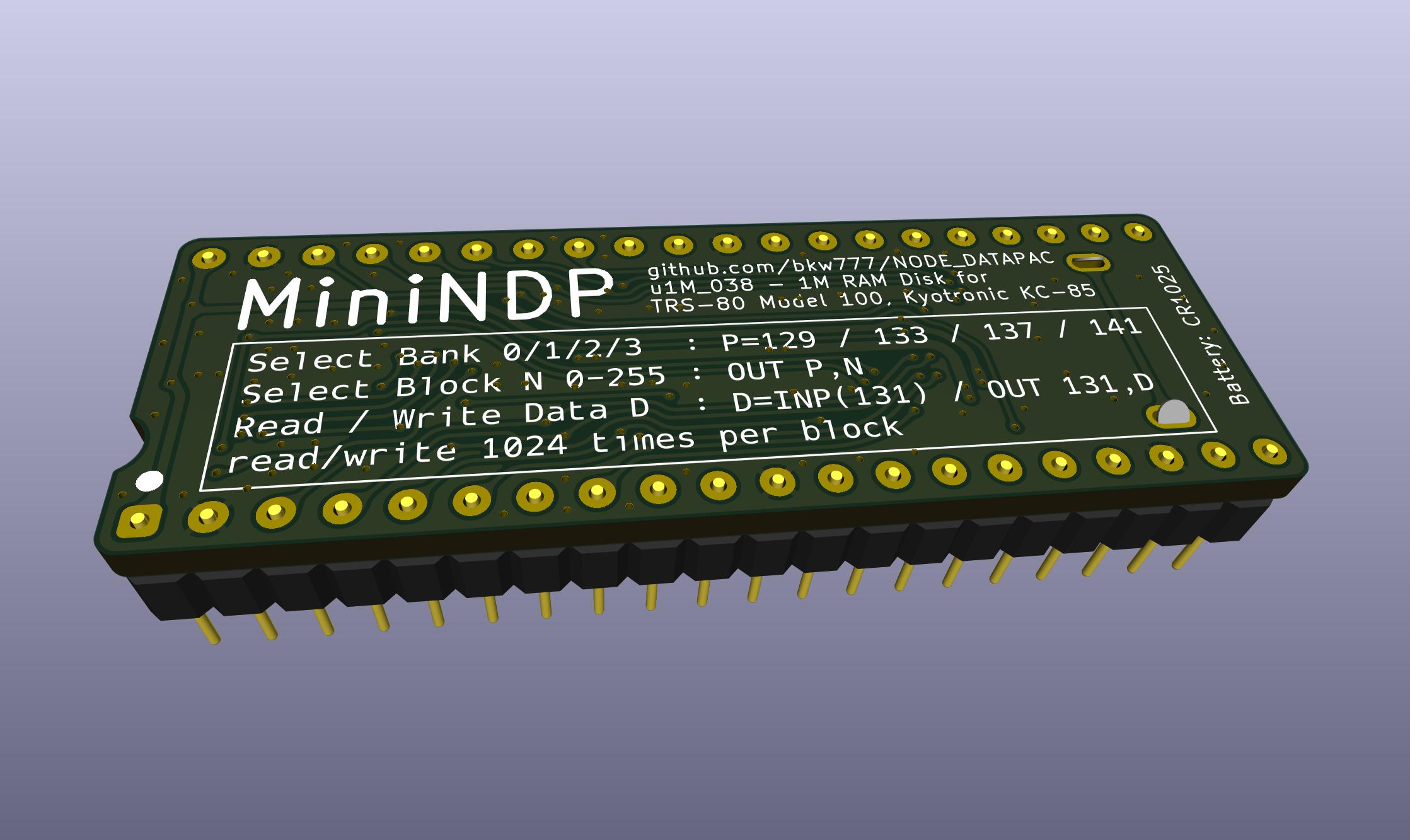
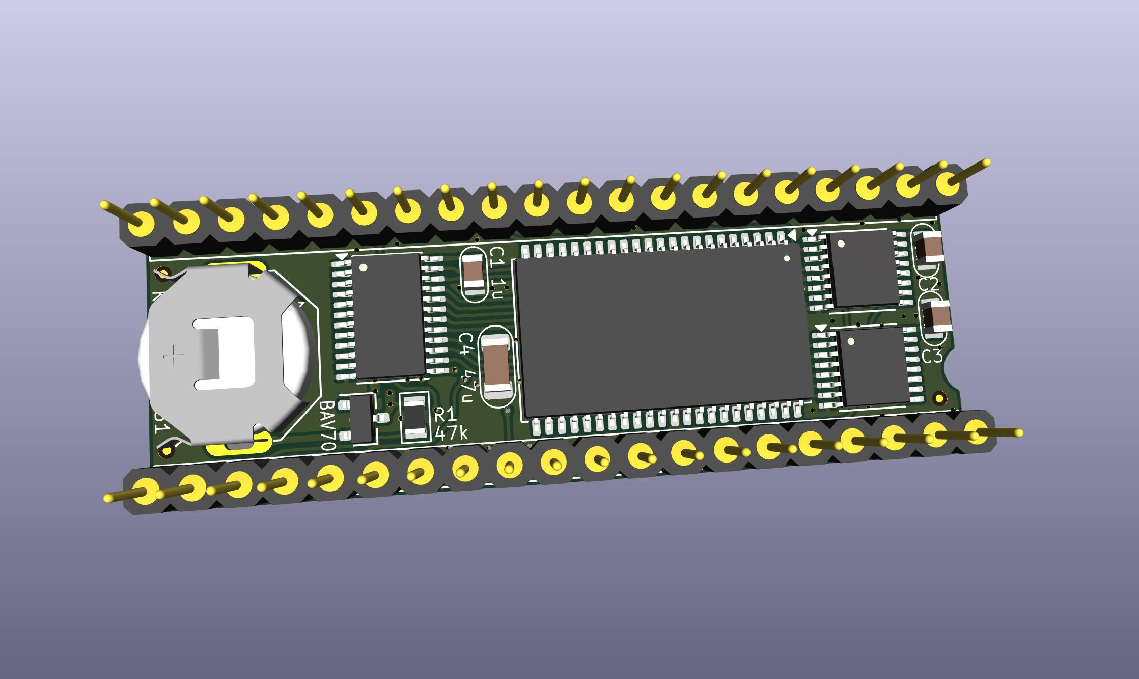
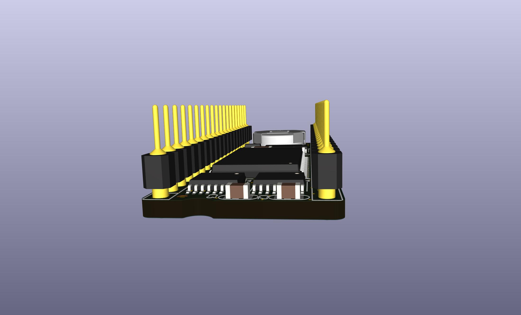
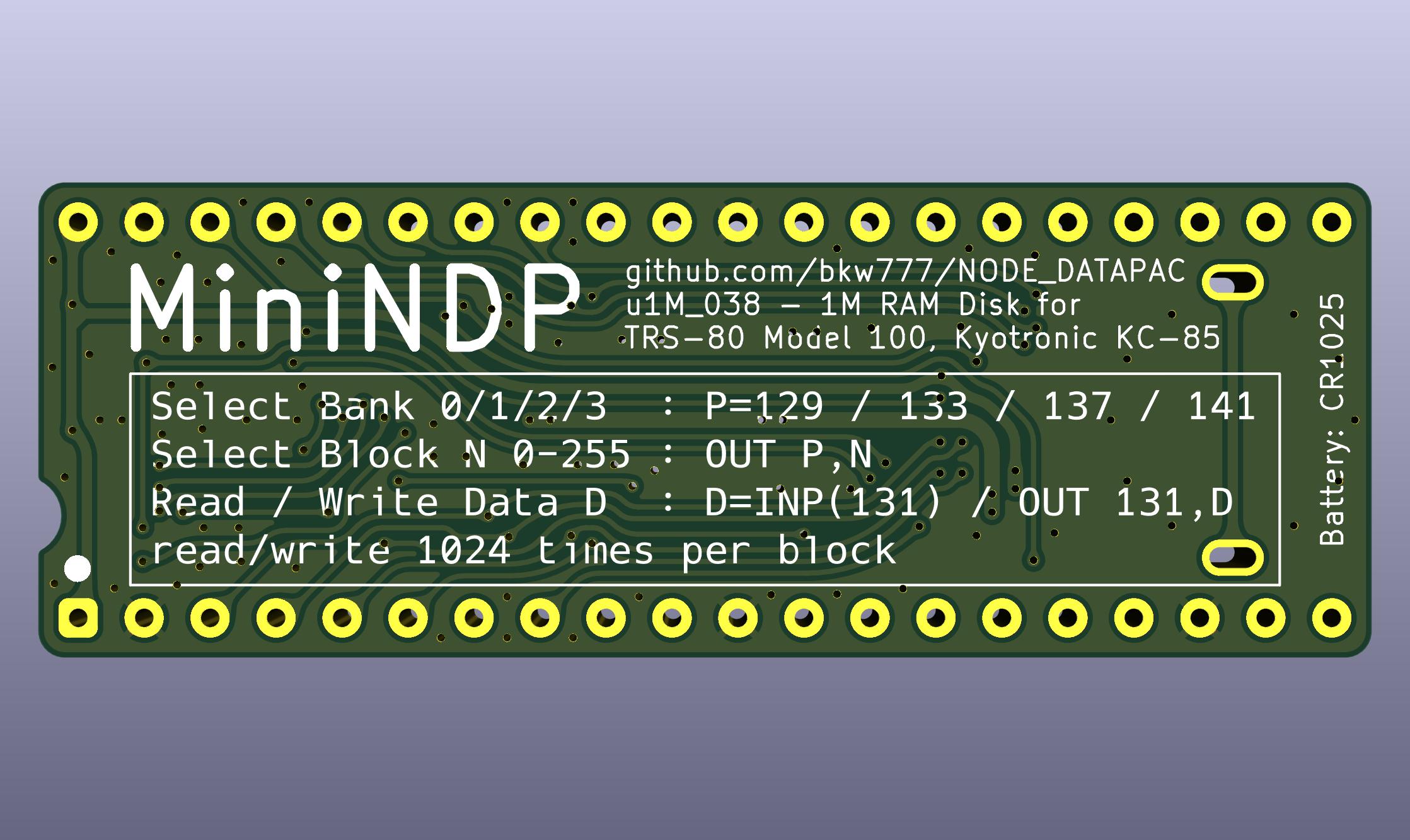
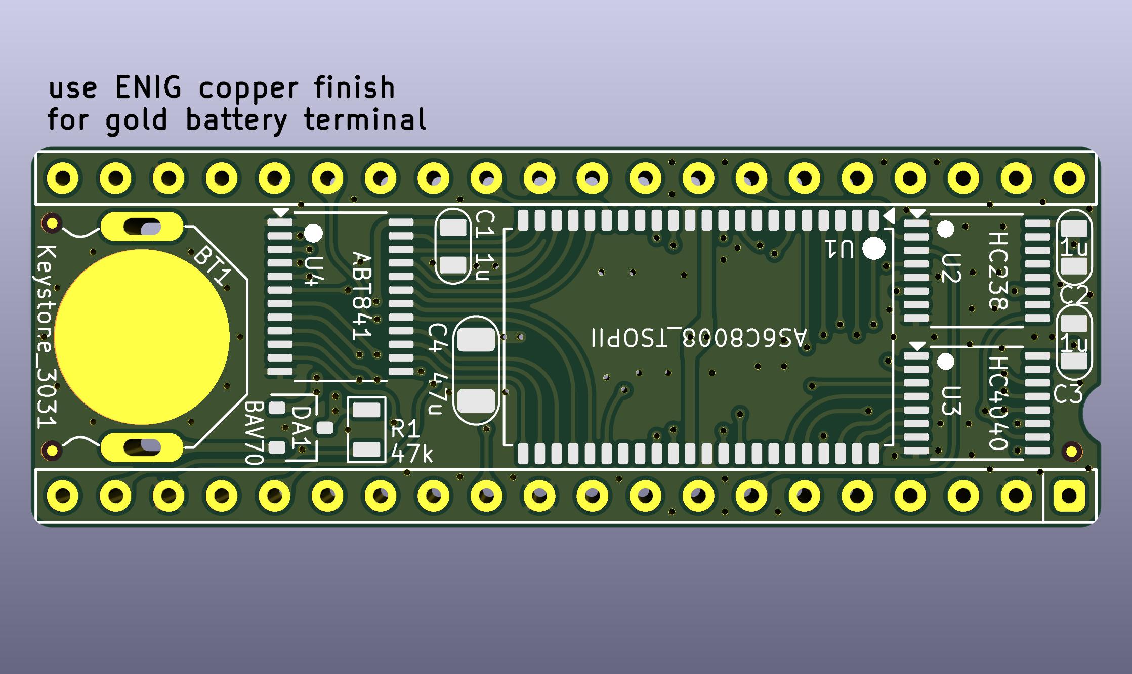
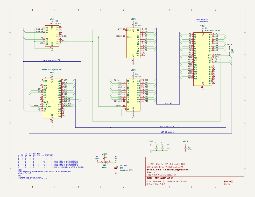
BOM: MiniNDP_u1M.bom.csv
MiniNDP u1M_038 PCB @ OSHPark
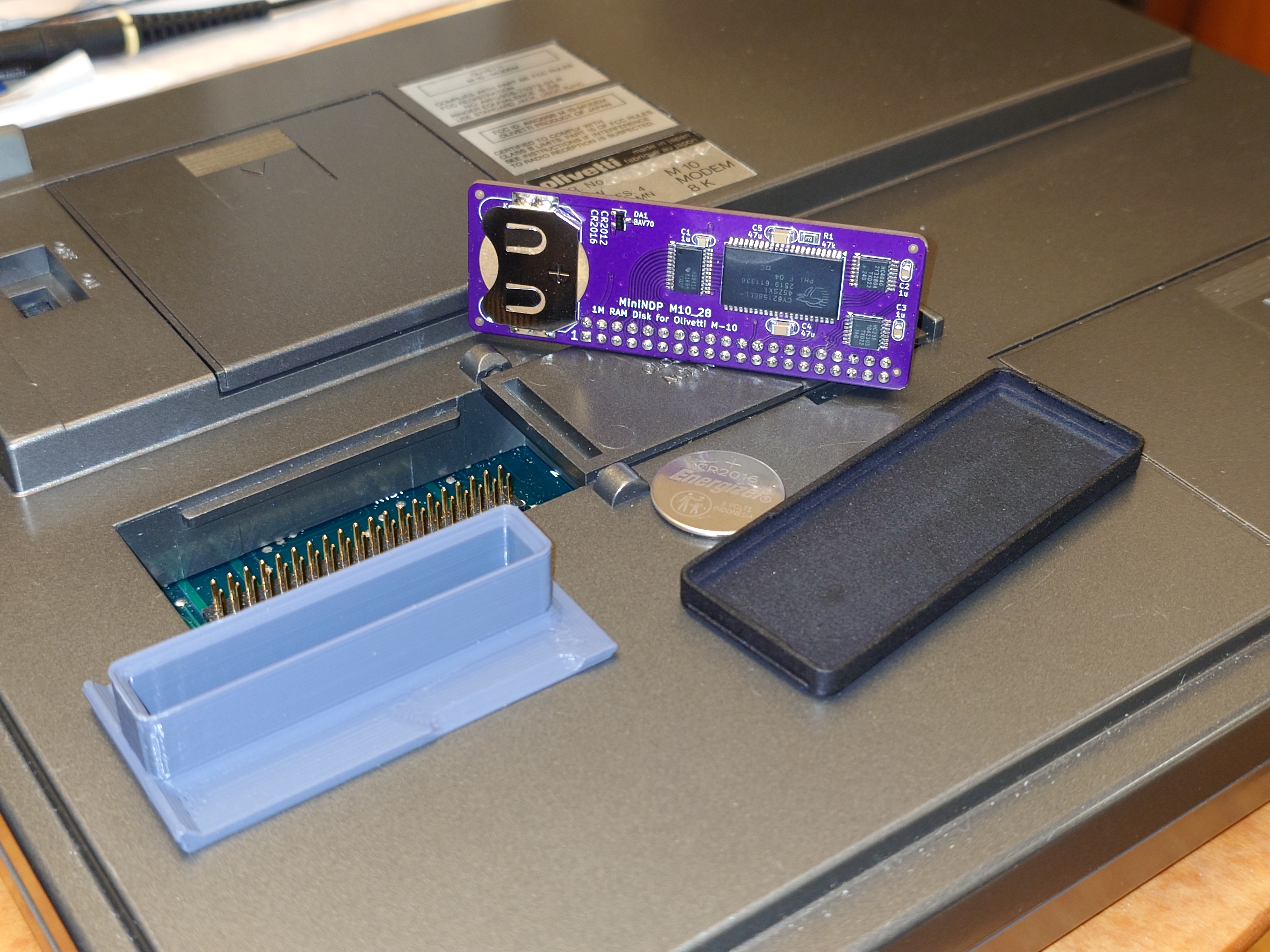
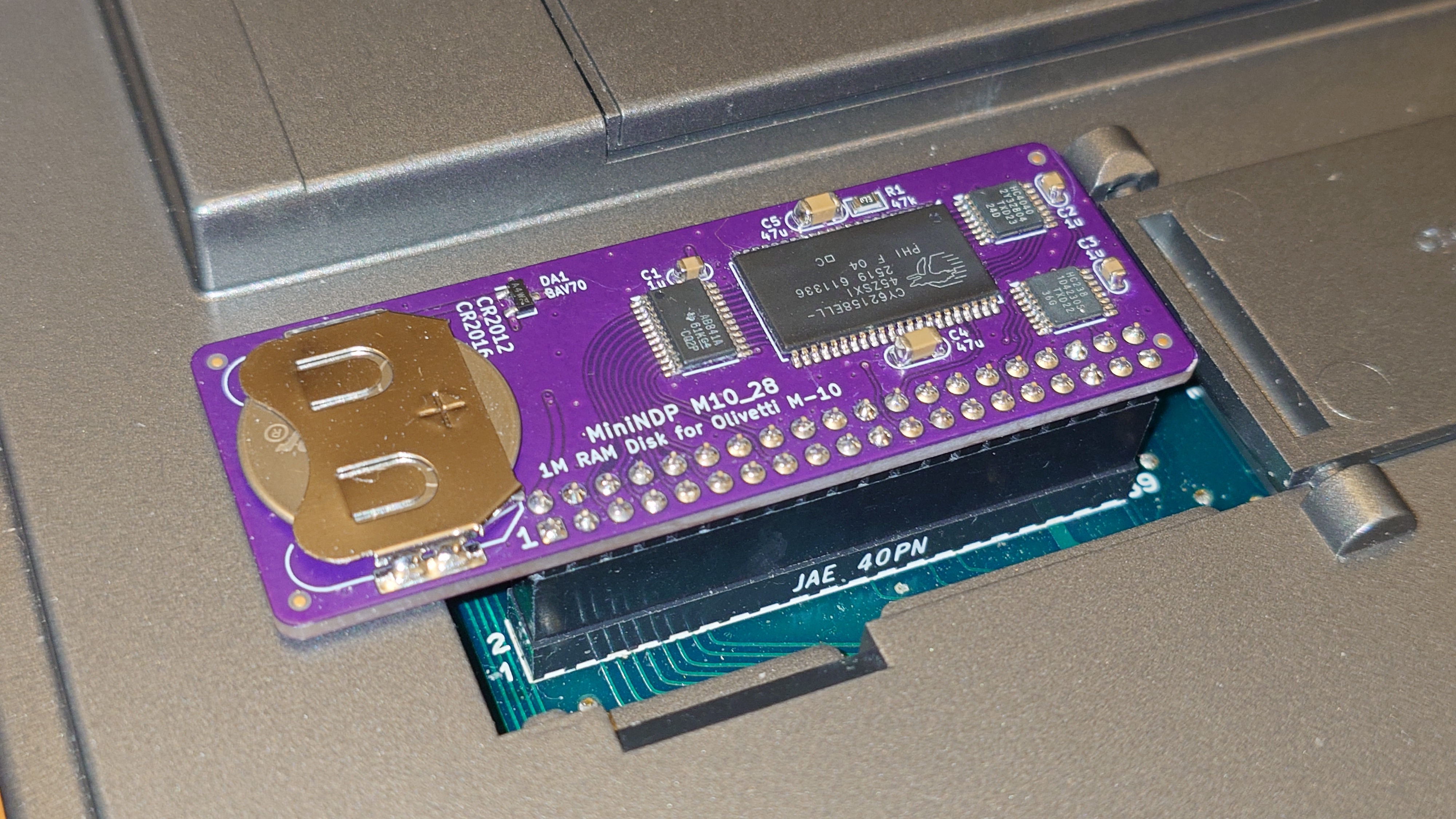
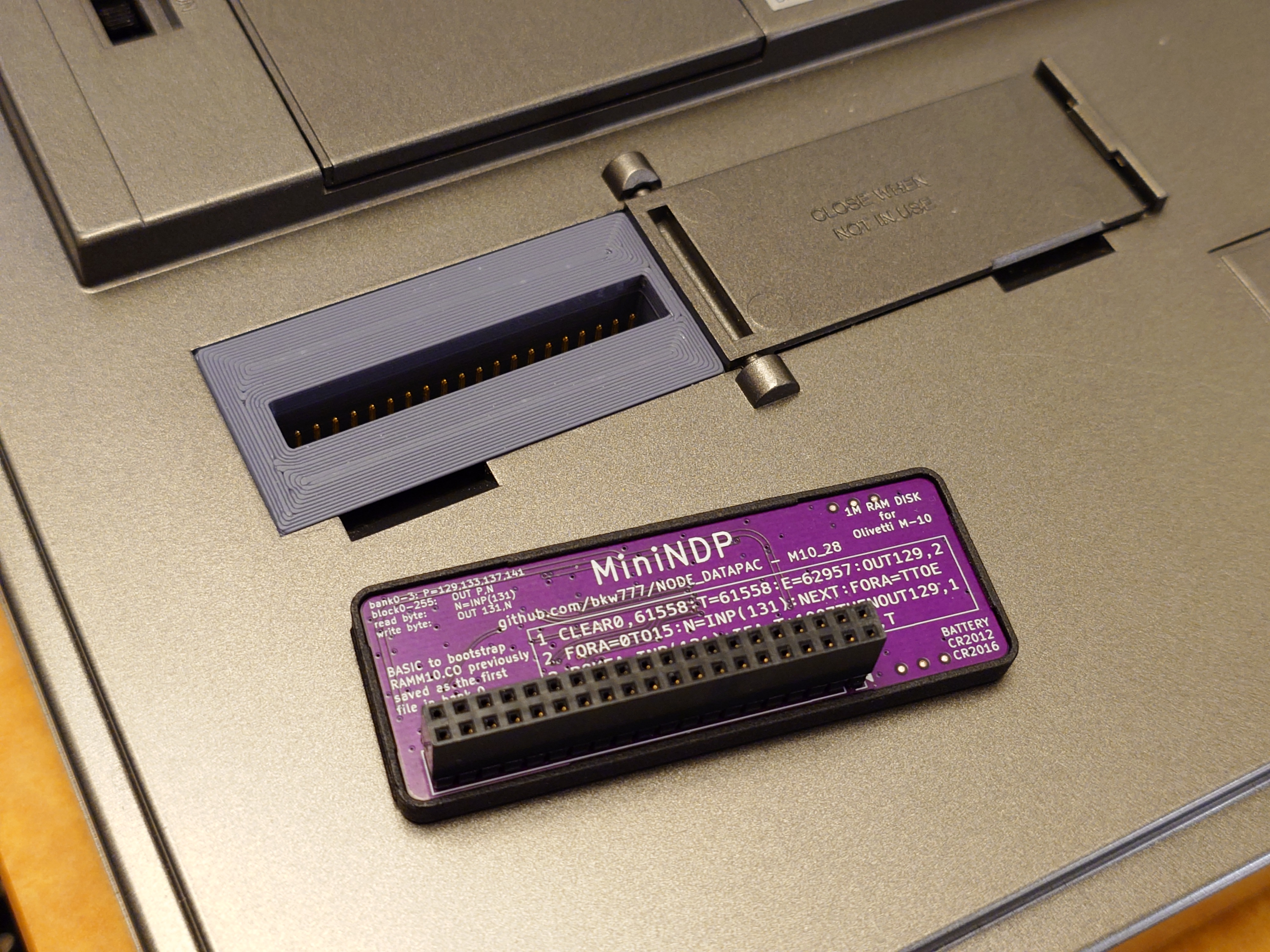
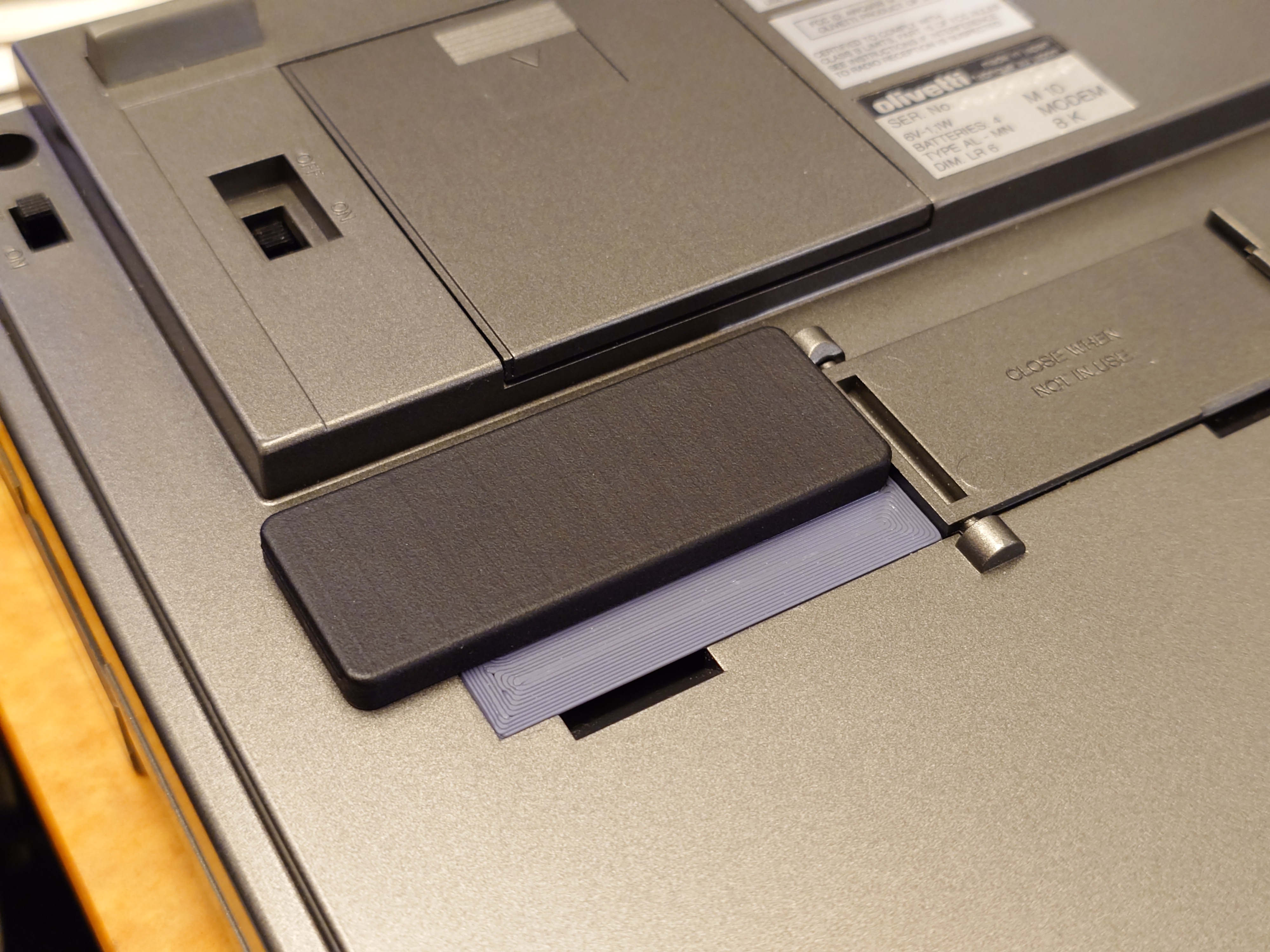
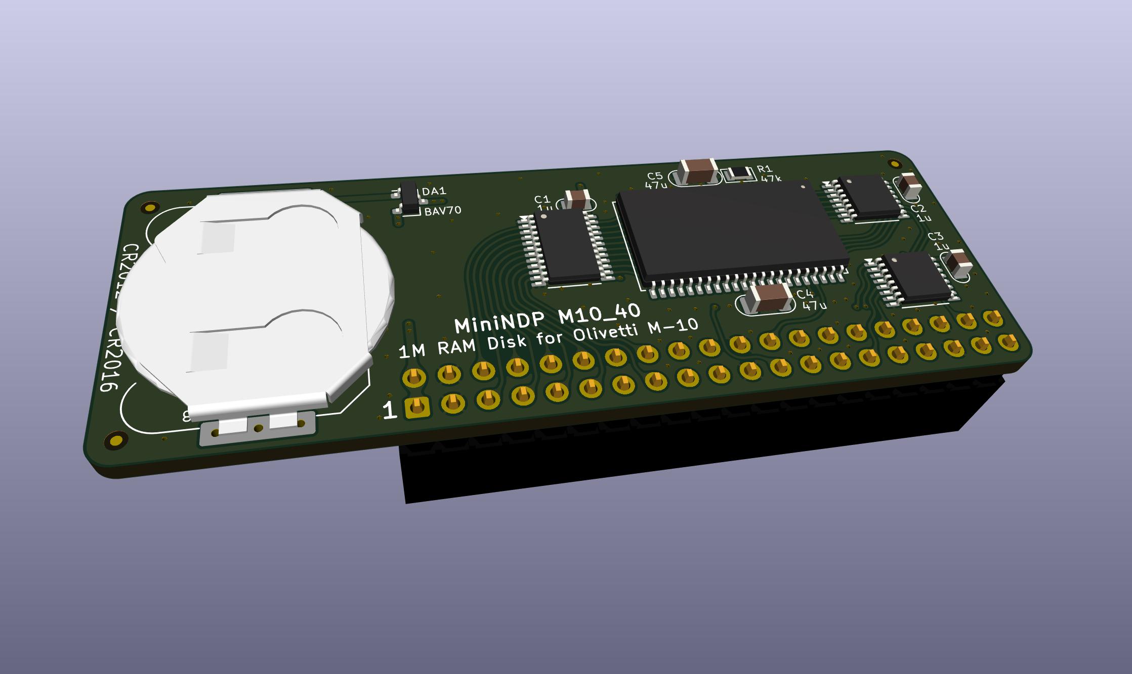
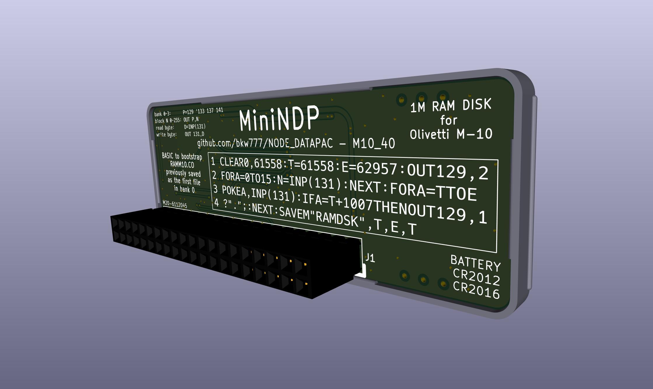
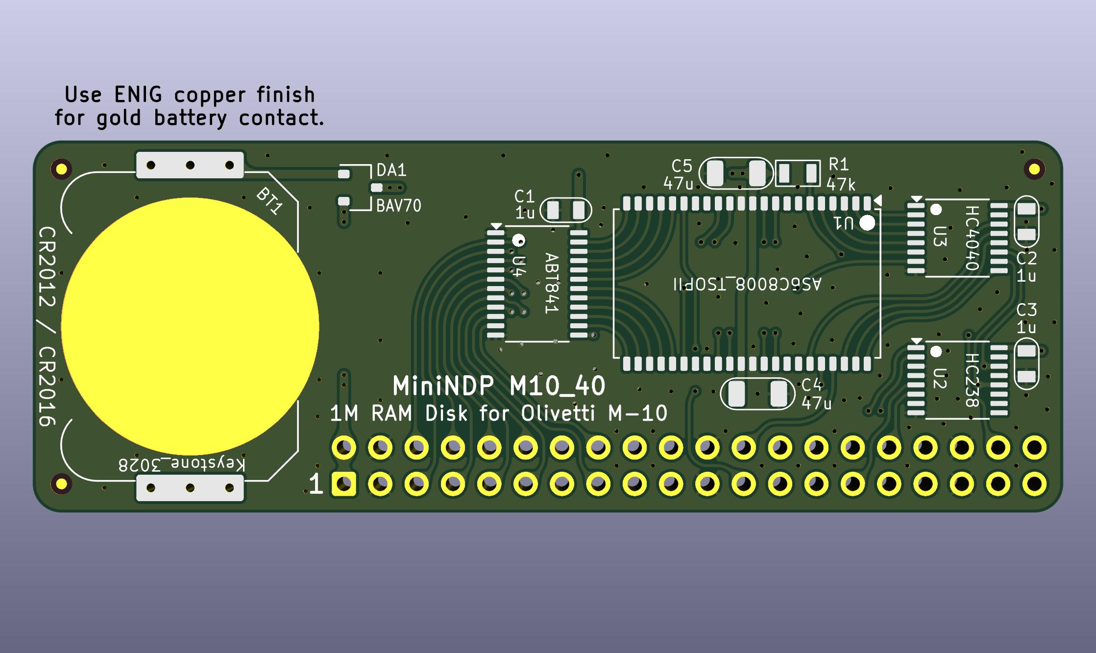
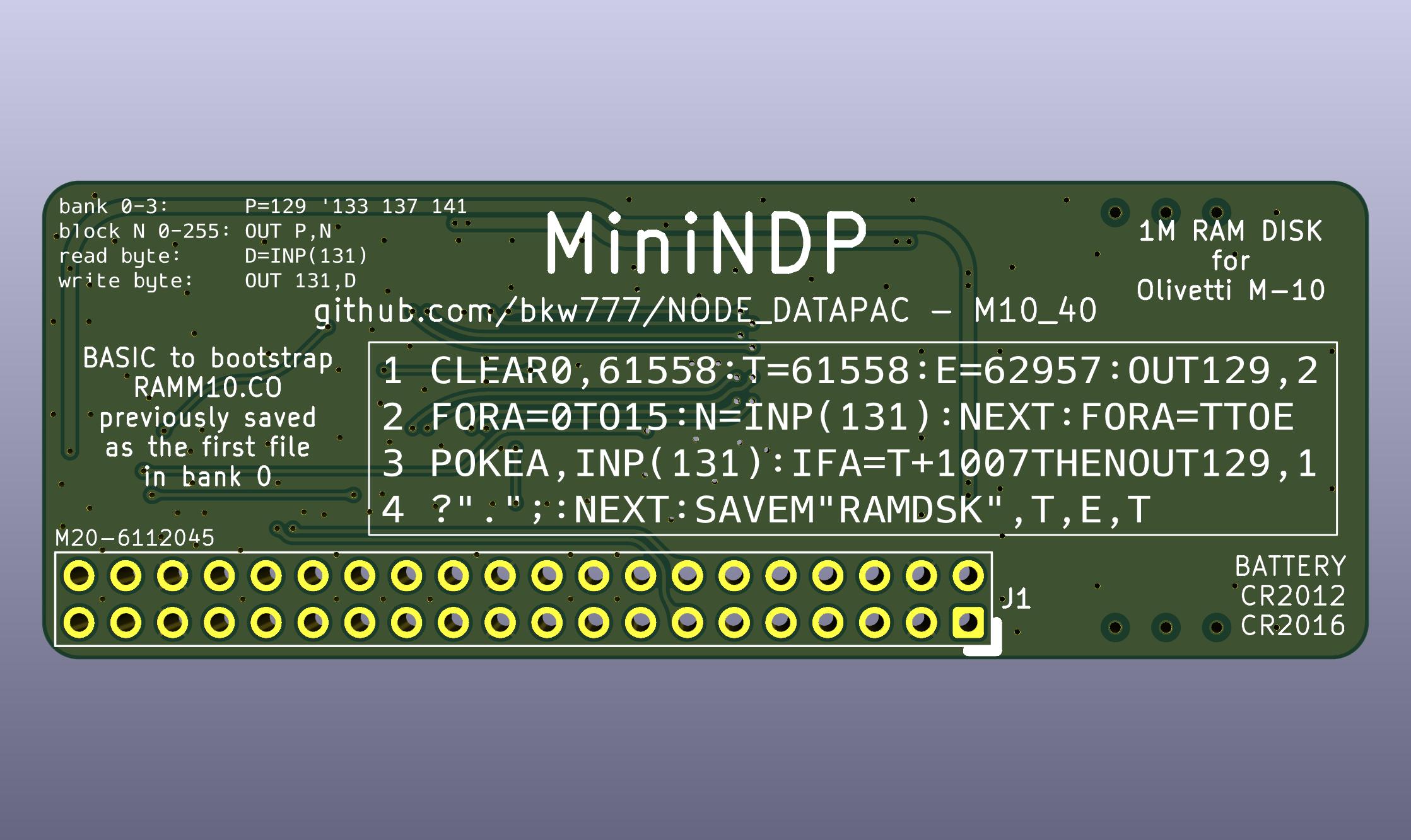
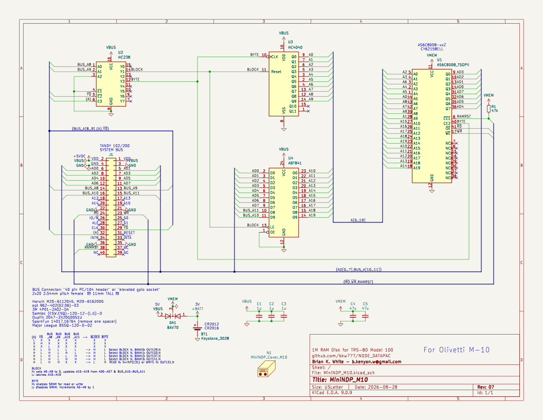
BOM: MiniNDP_M10.bom.csv
MiniNDP M10_40 PCB @ OSHPark
Cover for M10: MiniNDP_Cover_M10.stl -- M10 Cover @ JawsTec
Bus connector guide & filler plate for M10 M10_BUS_Filler_Plate.stl
SL1M - slim 1 meg, all thin chips to make a thin card
T512 - TSOP 128k/256k/512k
EZ512 - SOIC 512k
| Qty | Value | Footprint | References |
|---|---|---|---|
| 7 | 1u | 000_LOCAL:C_cer_tht_p2.5 | C1, C2, C3, C4, C5, C6, C7 |
| 4 | 62256 | 000_LOCAL:DIP-28_W15.24mm | U7, U8, U9, U10 |
| 3 | 1N4148 | 000_LOCAL:D_DO-35_SOD27_P10.16mm_Horizontal | D1, D2, D3 |
| 3 | HC161 | 000_LOCAL:DIP-16_W7.62mm | U1, U2, U3 |
| 3 | MountHole | 000_LOCAL:MountingHole_3.2mm_M3_Pad | H1, H2, H3 |
| 2 | HC138 | 000_LOCAL:DIP-16_W7.62mm | U4, U5 |
| 1 | 240k | 000_LOCAL:R_Axial_DIN0207_L6.3mm_D2.5mm_P10.16mm_Horizontal | R3 |
| 1 | 5.1k | 000_LOCAL:R_Axial_DIN0207_L6.3mm_D2.5mm_P10.16mm_Horizontal | R2 |
| 1 | CR2032 | 000_LOCAL:BH-25x-x | BT1 |
| 1 | Conn_02x20_Odd_Even | 000_LOCAL:IDC_to_board_2x20 | J1 |
| 1 | HC374 | 000_LOCAL:DIP-20_W7.62mm | U6 |
| 1 | U11_~{CS} | 000_LOCAL:TP_THT | TP1 |
| 1 | U12_~{CS} | 000_LOCAL:TP_THT | TP2 |
| 1 | U13_~{CS} | 000_LOCAL:TP_THT | TP3 |
| 1 | U14_~{CS} | 000_LOCAL:TP_THT | TP4 |
bkw777/NODE_DATAPAC
Reproduction & documentation of Node Systems DATAPAC


bkw777/NODE_DATAPAC
Reproduction & documentation of Node Systems DATAPAC

cazacov/PocketComputers
My experiments with programmable calculators and pocket computers


It measures 255.3 × 43.2 mm and has 2 copper layers, 1.6 mm thick.
31 parts, built around the HC138 and CR2032. The full list of its parts is on this page, with links to each part's symbol and footprint where PCBKit's library has them.
From the bkw777/NODE_DATAPAC repository on GitHub, at the commit this page was made from: the board is PCB/NODE_DATAPAC_256K_bkw.kicad_pcb and its schematic PCB/Control_Logic_Reference.kicad_sch. PCBKit opens the board in the browser, with nothing to install.
Its repository states no licence, so its author keeps all rights: ask bkw777 before reusing the design.