4 layers40.3 × 68.8 mm

 besi/esp8266-pcb1
The 16MB flash chip need some special settings when flashing:
Esp8266 is an open-source printed circuit board by besi, from the besi/esp8266-pcb repository on GitHub. It is a 2-layer board of 55.1 × 26 mm with 47 parts on 58 nets, routed with 497 tracks and 145 vias.
It is built around the CH340C, ESP8266EX and HDC1080DMBR, with the W25Q128JVSIQ TR, AP2112K-3.3TRG1(MS) and MCP73831T-2ACI/OT-HXY among its other parts. Its parts include 11 ICs, 10 capacitors, 9 resistors, 2 connectors and 2 inductors. It belongs with the ESP8266 boards of this library.


The 16MB flash chip need some special settings when flashing:
esptool.py -p /dev/cu.usbserial-1412440 \
-c esp8266 -b 460800 write_flash -fm dio \
--flash_size=16MB \
0x0000 ~/Downloads/ESP8266_GENERIC-20240222-v1.22.2.bin \
0xffc000 ~/esp/esp-idf/components/esptool_py/esptool/test/images/esp8266_sdk/esp_init_data_default.bin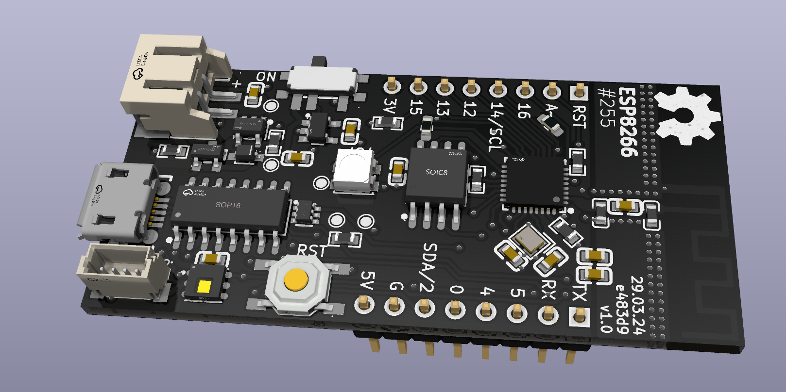
I created the following alias to download the footprints:
# ~/.zshrc
alias jlc='JLC2KiCadLib -dir lib -symbol_lib jlc_symbols -symbol_lib_dir "." -footprint_lib jlc_footprints.pretty'
So I can for example run jlc C123455 to download both the symbol and the footprint for a given component.
jlc C77967 --no_symbol # ESP8266EX chip
jlc C505111 --no_symbol # Micro USB adapter
jlc C7464026 --no_symbol # USB2UART chip
jlc C160390 # I2C connector
jlc C82227 # Temperature and humidity sensor
jlc C2922787 # SK6812 Neopixel
jlc C51118 # 3V3 AP2112K voltage regulator
jlc C62892 # NPN transistor array
jlc C318884 # Tactile switches
jlc C424093 # Battery management IC
jlc C97521 # flash chip (alternative: C5127618)
jlc C295747 # JST battery connector
jlc C963206 # slide switch
jlc C15127 # FET for switching between VUSB and VBAT
jlc C155590 # Zener Diode D3

jlc C22975 # 2k R4
jlc C19666 # 4.7uF
jlc C25804 # 10k
jlc C155590 # Shottkydiode D3
jlc C15127 # p channel mosfet
jlc C15849 # 1uF
jlc C23630 # 2.2uF
jlc C19702 # 10uF| Qty | Value | Footprint | References |
|---|---|---|---|
| 5 | TestPoint | TestPoint:TestPoint_Pad_D1.0mm | TP1, TP4, TP5, TP6, TP9 |
| 4 | 10k | jlc_footprints:R0603 | R3, R5, R6, R7 |
| 3 | 100n | jlc_footprints:C0603 | C2, C8, C10 |
| 2 | 10p | jlc_footprints:C0603 | C3, C4 |
| 2 | 2k | Resistor_SMD:R_0603_1608Metric_Pad0.98x0.95mm_HandSolder | R8, R9 |
| 2 | Conn_01x08 | Connector_PinHeader_2.54mm:PinHeader_1x08_P2.54mm_Vertical | J1, J2 |
| 2 | DNP | jlc_footprints:L0603 | L1, L2 |
| 1 | + | jlc_footprints:CONN-SMD_P2.00_S2B-PH-SM4-TB-LF-SN | U7 |
| 1 | 10u | jlc_footprints:C0603 | C1 |
| 1 | 12k | jlc_footprints:R0603 | R1 |
| 1 | 1u | jlc_footprints:C0603 | C7 |
| 1 | 2.2u | jlc_footprints:C0603 | C9 |
| 1 | 200 | jlc_footprints:R0603 | R2 |
| 1 | 26Mhz | jlc_footprints:CRYSTAL-SMD_4P-L2.0-W1.6-BL | Y1 |
| 1 | 2k | jlc_footprints:R0603 | R4 |
| 1 | 4.7u | jlc_footprints:C0603 | C5 |
| 1 | 5.6p | jlc_footprints:C0603 | C6 |
| 1 | AO3401A | jlc_footprints:SOT-23_L2.9-W1.3-P1.90-LS2.4-BR | Q1 |
| 1 | AP2112K-3_3TRG1 | jlc_footprints:SOT-25-5_L2.9-W1.6-P0.95-LS2.8-BL | U3 |
| 1 | Antenna_Trace | RF_Antenna:Texas_SWRA117D_2.4GHz_Right | E2 |
| 1 | BAT20JFILM | jlc_footprints:SOD-323_L1.8-W1.3-LS2.5-RD | D3 |
| 1 | BM04B-SRSS-TB(LF)(SN) | jlc_footprints:CONN-SMD_BM04B-SRSS-TB | REF1 |
| 1 | CH340C | jlc_footprints:SOP-16_L10.0-W3.9-P1.27-LS6.0-BL | U13 |
| 1 | ESP8266EX | jlc_footprints:QFN-32_L5.0-W5.0-P0.50-BL-EP3.7 | U2 |
| 1 | HDC1080DMBR | jlc_footprints:SENSOR-SMD_HDC1080DMBR | U4 |
| 1 | MCP73831T-2ACI_OT | jlc_footprints:SOT-23-5_L3.0-W1.7-P0.95-LS2.8-BL | U5 |
| 1 | ON | jlc_footprints:SW-SMD_MK-12C02-G020 | U6 |
| 1 | RST | jlc_footprints:SW-SMD_4P-L5.1-W5.1-P3.70-LS6.5-TL-2 | U10 |
| 1 | SK6812MINI-HS | jlc_footprints:LED-SMD_4P-L3.5-W3.5-BR_SK6812MINI-HS | U8 |
| 1 | UMH3N | jlc_footprints:SC-70-6_L2.2-W1.3-P0.65-LS2.1-BR | U9 |
| 1 | USB_B_Micro | jlc_footprints:MICRO-USB-SMD_1050171001 | JP1 |
| 1 | W25Q128JVSIQTR | jlc_footprints:SOIC-8_L5.3-W5.3-P1.27-LS8.0-BL | U11 |
| 1 | deep-sleep | Jumper:SolderJumper-2_P1.3mm_Open_TrianglePad1.0x1.5mm | JP2 |
| 1 | locked | Symbol:OSHW-Symbol_6.7x6mm_SilkScreen | OSHW1 |

CodeSakshamY/Half-life-HackClub
custom pcb for my psycon wearable project. designed in easyeda.

stevfu/eis_capstone
Utilization of Electrochemical Impedance Spectroscopy for the Detection of Drugs


rogerclarkmelbourne/STM32_Pill_Boards
Various STM32 boards in a form factor similar to the Maple Mini or Blue Pill board
It measures 55.1 × 26 mm and has 2 copper layers, 1.6 mm thick.
47 parts, built around the CH340C, ESP8266EX, HDC1080DMBR and W25Q128JVSIQ TR. The full list of its parts is on this page, with links to each part's symbol and footprint where PCBKit's library has them.
From the besi/esp8266-pcb repository on GitHub, at the commit this page was made from: the board is esp8266.kicad_pcb and its schematic esp8266.kicad_sch. PCBKit opens the board in the browser, with nothing to install.
Its repository states no licence, so its author keeps all rights: ask besi before reusing the design.