2 layers96 × 26 mm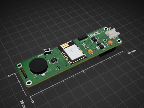

 bansalsaksham/PressLog1
Manufacturing-ready PCB design for an industrial IoT downtime-logging edge node. Offline-first firmware architecture, KiCad schematics, Gerbers, and BOM.
PressLog Edge Node is an open-source printed circuit board by bansalsaksham, from the bansalsaksham/PressLog repository on GitHub. It is a 2-layer board of 117 × 81.5 mm with 45 parts on 52 nets, routed with 286 tracks and 10 vias.
It is built around the ESP32-S3-WROOM-1-N8, LM2596S-5.0 and AMS1117, with the DS3231MZ+ among its other parts. Its parts include 16 resistors, 14 capacitors, 7 connectors, 4 ICs and 2 diodes. It belongs with the home automation and IoT boards and the ESP32 boards of this library.


A manufacturing-ready PCB and firmware architecture for capturing machine downtime reasons on a factory floor.
Origin: The original design brief (see
Original Case Study Brief.pdf) was given as a second-round technical case study during an internship interview process. I completed the full PCB design and firmware architecture independently and am sharing it here as my own project.
Status: PCB design and firmware architecture complete. DRC/ERC clean, Gerbers and BOM generated for fabrication. Not yet physically built/soldered — this repository documents the design and engineering rationale, not a deployed product.
OEE (Overall Equipment Effectiveness) is only as good as its data. But capturing downtime reasons at the machine edge is a human-interface problem as much as a software one. The factory floor kills conventional UX.
| Constraint | Root Cause | Why Standard Solutions Fail |
|---|---|---|
| Gloved hands | Thick Kevlar + metallic dust make capacitive screens useless | Tablet solutions require bare fingers: 15–30s to glove off/on. Fails the 5-second window. |
| Patchy Wi-Fi | VFDs, metal shielding, and RF interference create 2-hour dead zones | Cloud-first designs lose events silently. Operator never knows. OEE has invisible gaps. |
| 5-second window | Operator moves to the next task seconds after a machine stops | Any UI requiring navigation or multiple confirmations is abandoned. |
device_id, machine_id, reason_code, operator_uid (NFC badge tap), UTC timestamp, and a sequence number. Sequence gaps are auto-detected downstream so any connectivity hole is visible to plant management.Designed specifically for high-noise industrial environments.
| Engineering Decision | Why It Matters |
|---|---|
| RC hardware debounce matrix (10kΩ/0.1µF) on all 6 inputs | Software-only debouncing fails near VFDs and heavy machinery — this prevents ghost button events at the hardware level |
| Isolated I2C routing for DS3231 RTC | Routed completely clear of the 150kHz buck converter switching node — prevents inductive noise from corrupting timestamps. If the timestamp is wrong, the offline queue is worthless. |
| DFM: thermal vias 0.2mm → 0.3mm | Standard drill size reduces fabrication cost without sacrificing thermal performance |
| RF-notched board edge | Lets the ESP32 antenna hang off the fiberglass substrate, preventing signal attenuation |
| Component | Specification |
|---|---|
| Platform | ESP32-S3, dual-core 240MHz |
| Buttons | 6× 30mm illuminated tactile (5N actuation) |
| Connectivity | Wi-Fi 802.11n + BLE 5.0 |
| Offline queue | 8MB LittleFS (~65,000 events) |
| RTC | DS3231, ±2ppm, coin-cell backup |
| Power | 24VDC input + 2000mAh LiPo backup (8h) |
| Identity | PN532 NFC module |
Offline-first data flow:
Button Press → RTC Timestamp → Flash Queue (always written first) → Wi-Fi Check → Cloud Sync (batch HTTPS POST)Defense-in-depth: the hardware RC filter kills high-frequency spikes; a 50ms software debounce is the secondary safety net.
// Button ISR with secondary 50ms software debounce
void IRAM_ATTR isr_btn_0() {
  uint32_t now = millis();
  if (!pressed[0] && (now - last[0]) > 50) {
    pressed[0] = true;
    last[0] = now;
  }
}

// Queue write — always before network attempt
queueWrite(seq, rtc.now().unixtime(), buttonIdx); // flash first
confirmFeedback(buttonIdx);                       // LED + buzzer + vibration
if (wifiOnline) syncQueue();                       // attempt immediate sync
Event payload schema:
{
  "device_id": "DL-CNC07-A3",
  "seq": 1042,
  "ts": "2026-04-08T14:22:08Z",
  "ts_source": "rtc",
  "reason_code": "MATERIAL_JAM",
  "reason_label": "Material Jam",
  "operator_uid": "a3f9d82c",
  "machine_id": "CNC-07"
}├── Hardware_Source/ # KiCad project — schematics + PCB layout
│ ├── ESP32_Core.kicad_sch
│ ├── HMI_IO.kicad_sch
│ ├── Power_Delivery.kicad_sch
│ ├── RTC_SubSystem.kicad_sch
│ └── PressLog_Edge_Node.kicad_pcb / .kicad_pro
├── Manufacturing/ # Fabrication-ready outputs
│ ├── PressLog_Gerbers/
│ └── PressLog_BOM.csv
├── Documentation/ # Renders, design rule reports, app mockups
│ ├── PressLog_Edge_Node.pdf
│ ├── DRC.rpt / ERC.rpt # Design Rule Check / Electrical Rule Check — board is verified manufacturable
│ ├── PressLog_Front.png / _Back.png / _Side.png
│ └── App Interface Designs.pdf
└── Original Case Study Brief.pdf # Full original case study writeupThis was a design and engineering reasoning exercise, not a built product. The PCB design itself is real, complete, and manufacturable.
Tools used: KiCad, ESP32-S3, LittleFS, DS3231 RTC, PN532 NFC
| Qty | Value | Footprint | References |
|---|---|---|---|
| 12 | 10k | Resistor_SMD:R_0805_2012Metric | R5, R6, R7, R8, R9, R10, R11, R12, R13, R14, R15, R16 |
| 8 | 0.1uF | Capacitor_SMD:C_0805_2012Metric | C6, C8, C9, C10, C11, C12, C13, C14 |
| 7 | Conn_01x02 | Connector_PinHeader_2.54mm:PinHeader_1x02_P2.54mm_Vertical | J1, J2, J3, J4, J5, J6, J7 |
| 3 | 10uF | Capacitor_SMD:C_0805_2012Metric | C3, C4, C5 |
| 2 | 10kΩ | Resistor_SMD:R_0805_2012Metric | R1, R2 |
| 2 | 4.7k | Resistor_SMD:R_0805_2012Metric | R3, R4 |
| 1 | 100uF | Capacitor_THT:CP_Radial_D10.0mm_P5.00mm | C1 |
| 1 | 1uF | Capacitor_SMD:C_0805_2012Metric | C7 |
| 1 | 220uF | Capacitor_THT:CP_Radial_D10.0mm_P5.00mm | C2 |
| 1 | 33uH | Inductor_SMD:L_12x12mm_H6mm | L1 |
| 1 | AMS1117 | Package_TO_SOT_SMD:SOT-223-3_TabPin2 | U2 |
| 1 | Battery_Cell | Battery:BatteryHolder_Keystone_1058_1x2032 | BT1 |
| 1 | DS3231M | Package_SO:SOIC-16W_7.5x10.3mm_P1.27mm | U4 |
| 1 | D_Schottky | Diode_SMD:D_SMA | D2 |
| 1 | D_TVS | Diode_SMD:D_SMA | D1 |
| 1 | ESP32-S3-WROOM-1 | RF_Module:ESP32-S3-WROOM-1 | U3 |
| 1 | LM2596S-5 | Package_TO_SOT_SMD:TO-263-5_TabPin3 | U1 |


jibonaronno/documentsA
It is required to change settings using SCLManager.exe when required for new setup.


It measures 117 × 81.5 mm and has 2 copper layers, 1.6 mm thick.
45 parts, built around the ESP32-S3-WROOM-1-N8, LM2596S-5.0, AMS1117 and DS3231MZ+. The full list of its parts is on this page, with links to each part's symbol and footprint where PCBKit's library has them.
From the bansalsaksham/PressLog repository on GitHub, at the commit this page was made from: the board is Hardware_Source/PressLog_Edge_Node.kicad_pcb and its schematic Hardware_Source/ESP32_Core.kicad_sch. PCBKit opens the board in the browser, with nothing to install.
Its repository states no licence, so its author keeps all rights: ask bansalsaksham before reusing the design.