
4 layers38.9 × 37.5 mm

 awesomeyooner/AS5047-Devboard
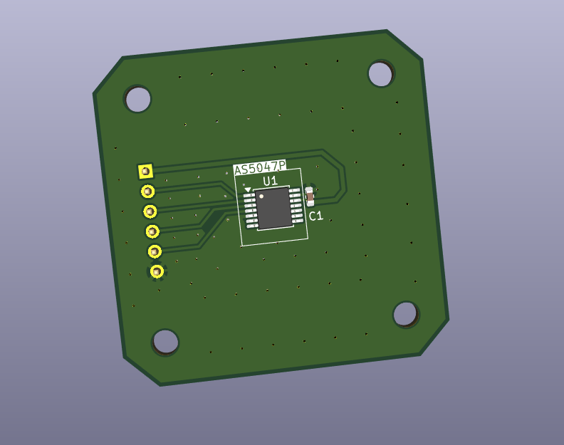
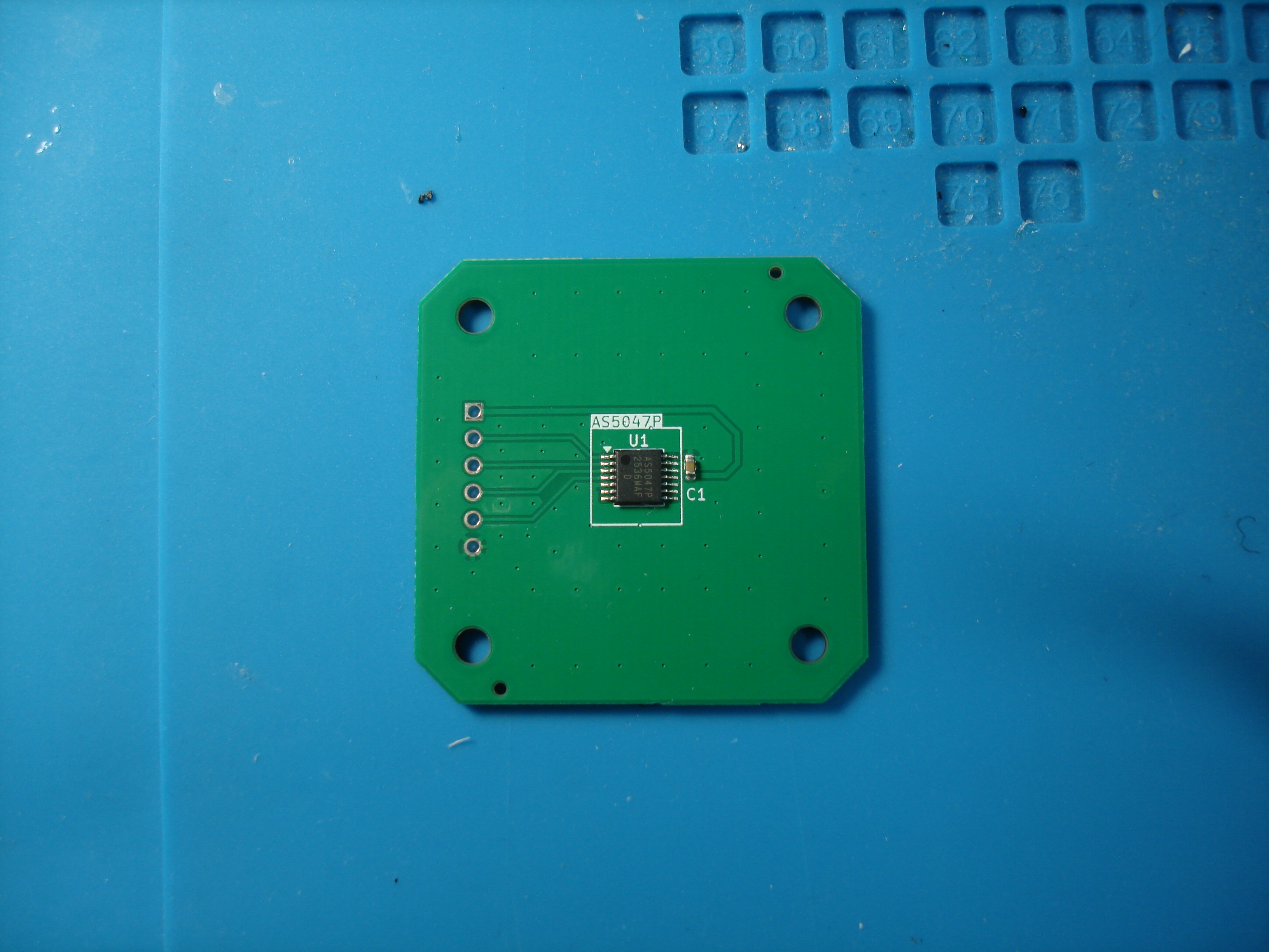
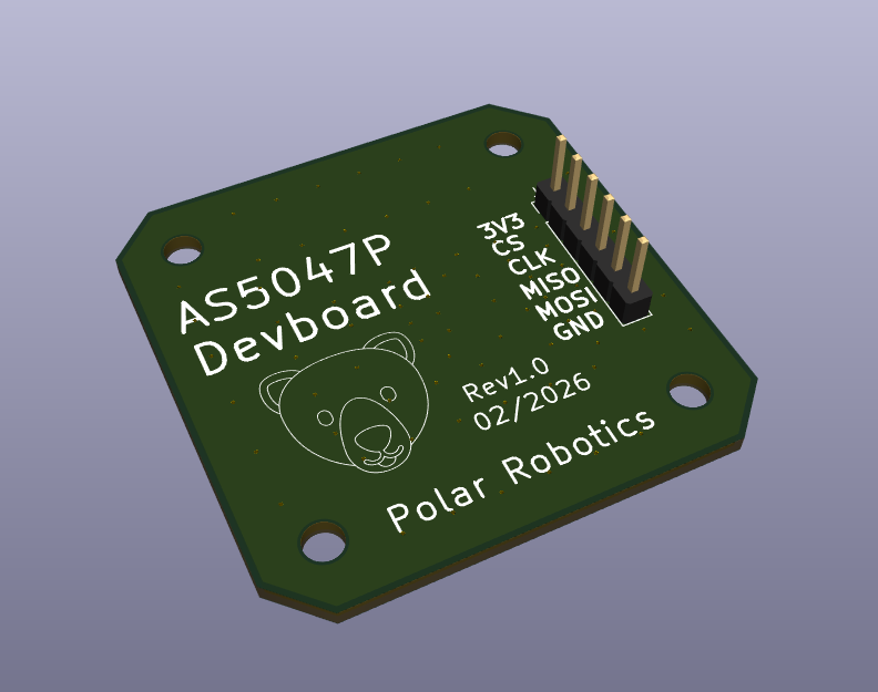
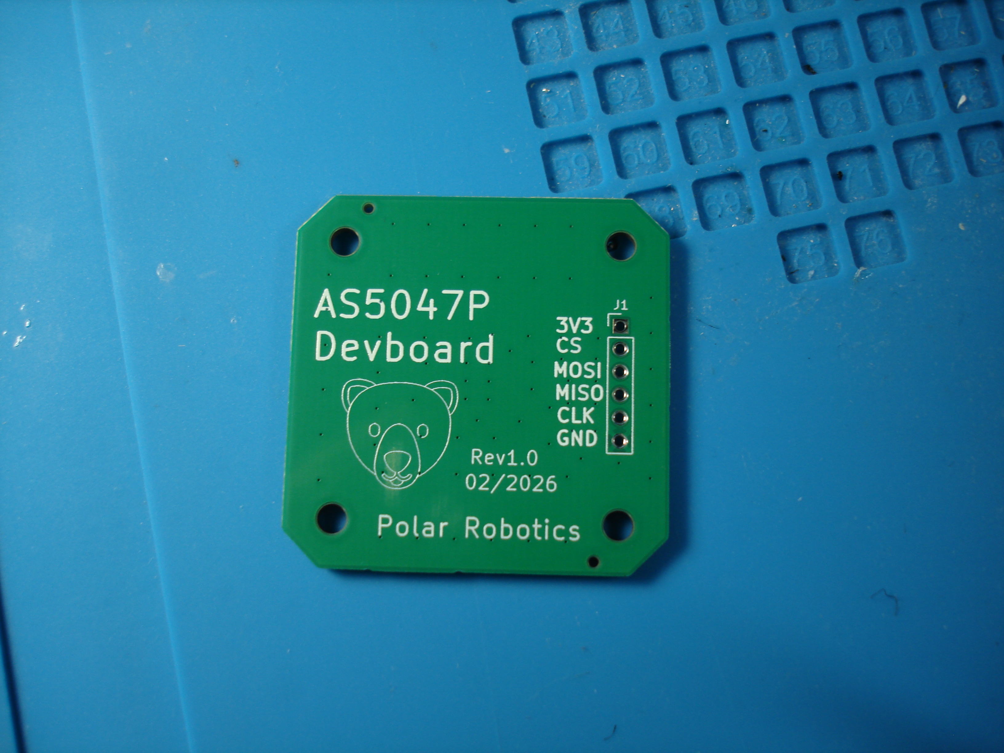
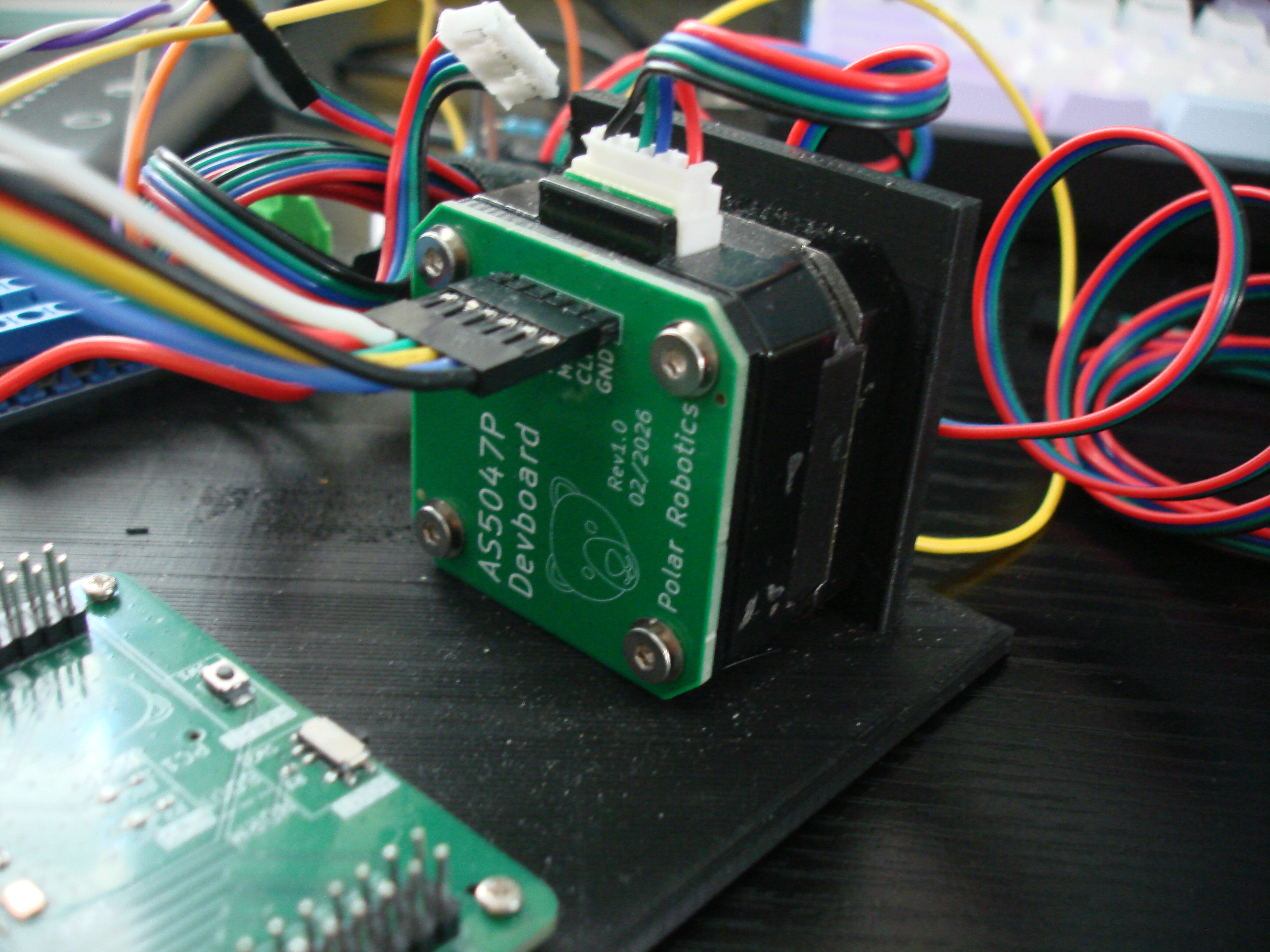
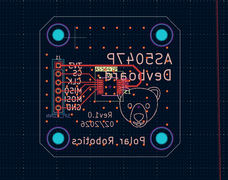
KiCAD project for breaking out the AS5047P magnetic encoder onto a NEMA17 hole pattern
AS5047-Devboard is an open-source printed circuit board by awesomeyooner, from the awesomeyooner/AS5047-Devboard repository on GitHub. It is a 2-layer board of 42 × 42 mm with 8 parts on 13 nets, routed with 27 tracks and 75 vias.
It is built around the AS5047P-AT. Its parts include 1 capacitor, 1 IC and 1 connector. It belongs with the microcontroller boards boards of this library.
KiCAD project for breaking out the AS5047P magnetic encoder onto a NEMA17 hole pattern. This is paired with Diametric Magnets from DigiKey
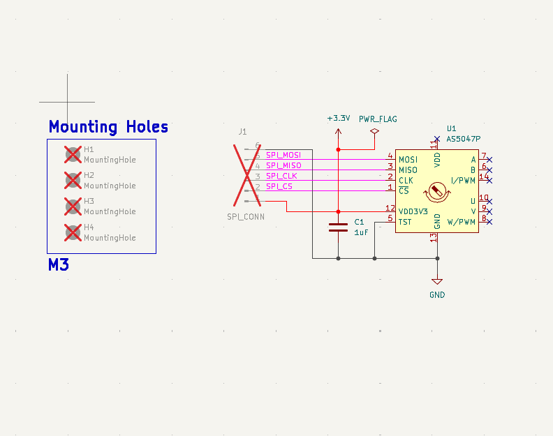
This only breaks out the SPI, since that is what my main purpose of it was. This is an incredibly simple PCB, and was ordered via JLCPCB
I ordered 5 assembled ones, and at the time the prices were
$35.41 total
| Qty | Value | Footprint | References |
|---|---|---|---|
| 4 | MountingHole | MountingHole:MountingHole_3.2mm_M3 | H1, H2, H3, H4 |
| 1 | 1uF | Capacitor_SMD:C_0603_1608Metric | C1 |
| 1 | AS5047P | Package_SO:TSSOP-14_4.4x5mm_P0.65mm | U1 |
| 1 | LOGO | LOGO | G*** |
| 1 | SPI_CONN | Connector_PinHeader_2.54mm:PinHeader_1x06_P2.54mm_Vertical | J1 |

Westly-Bouchard/AS5047P-Board
KiCad Project for an AS5047P Breakout Board


duwogus7650-ctrl/board-design
OpenRobot SPN-MC(=VESCular6, VESC6 파생) 동등 기능의 QDD용 원형 모터 컨트롤러를 오픈소스 VESC6를 베이스로 신규 설계하는 프로젝트.


niksrajendra/stm8-bootloader-extended
STM8 bootloader designed to work with any available communication interface and configure for different feature like secure, unsecure bootloader.


It measures 42 × 42 mm and has 2 copper layers, 1.6 mm thick.
8 parts, built around the AS5047P-AT. The full list of its parts is on this page, with links to each part's symbol and footprint where PCBKit's library has them.
From the awesomeyooner/AS5047-Devboard repository on GitHub, at the commit this page was made from: the board is pcb/AS5047-Devboard.kicad_pcb and its schematic pcb/AS5047-Devboard.kicad_sch. PCBKit opens the board in the browser, with nothing to install.
Its repository states no licence, so its author keeps all rights: ask awesomeyooner before reusing the design.