4 layers127 × 76.2 mm
Payload pcb
austindriggs/urc-payload-pcb
All-purpose control and interface board designed to manage mission-critical sensors and electronics for University Rover Challenge at WVU.
114 partsMIT

 austindriggs/spacex-sbc
Complete PCB architecture and design process for a custom SBC prepared for a technical interview presentation for a PCB Design Engineer at SpaceX before I graduated from WVU.
Spacex sbc is an open-source printed circuit board by austindriggs, from the austindriggs/spacex-sbc repository on GitHub. It is an 8-layer board of 75 × 75 mm with 46 parts on 660 nets, routed with 67 tracks and 79 vias.
It is built around the ATSAMA5D21C-CU, MAX3221CPW and TPS5430DDA, with the MCP16501TE-E/RMB and FL0800011Q among its other parts. Its parts include 16 capacitors, 10 ICs, 6 resistors, 3 connectors and 2 diodes. It belongs with the computers and single-board computers boards and the STM32 and SAM D and SAM boards of this library.


This repository contains the complete PCB architecture and design process for a custom Single Board Computer (SBC), prepared for a technical interview presentation for a PCB Design Engineer at SpaceX before I graduated from WVU. It walks through component package selection, power budget calculations, SoC and DDR3 memory constraint analysis, and 8-layer stackup optimization.
Disclaimer: This project is an independent personal design exercise created solely for educational and portfolio demonstration purposes. It is not affiliated with, endorsed by, sponsored by, or associated with Space Exploration Technologies Corp. (SpaceX). All trademarks, logos, and brand names mentioned herein belong to their respective owners.
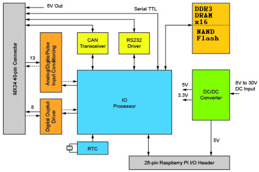
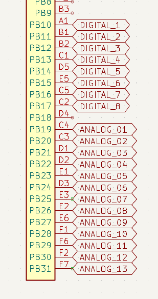
26 pin rpi GPIO: 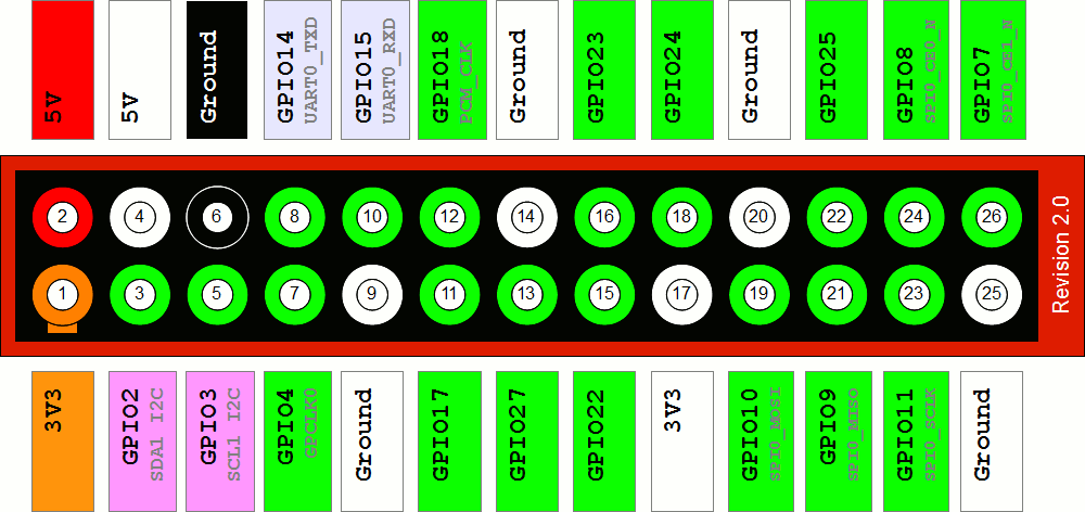
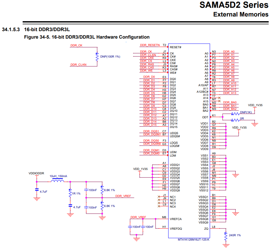
The DDR3 DRAM x16 is a single IC, so we won't need Fly-By-Topology (for addr and clk) and the extra layout space that two x8 ICs would take up.
Also assuming DDR3 and not DDR3L since that's what the block diagram is. DDR3 uses standard operating voltage of 1.5V (instead of L of 1.25V).
Also assuming that since its DDR3, it has On-Die-Termination (ODT) for the resistors.
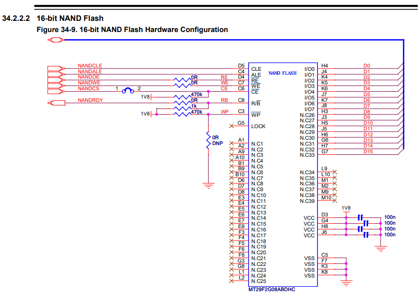
NAND Flash: can be 8 or 16 bit. For 8 bit, you can use the same IC but NC D8-D15. Note: Booting on 16-bit NAND Flash is not possible; only 8-bit NAND Flash memories are supported.
What is RS232? The RS-232 protocol by Ben Eater.
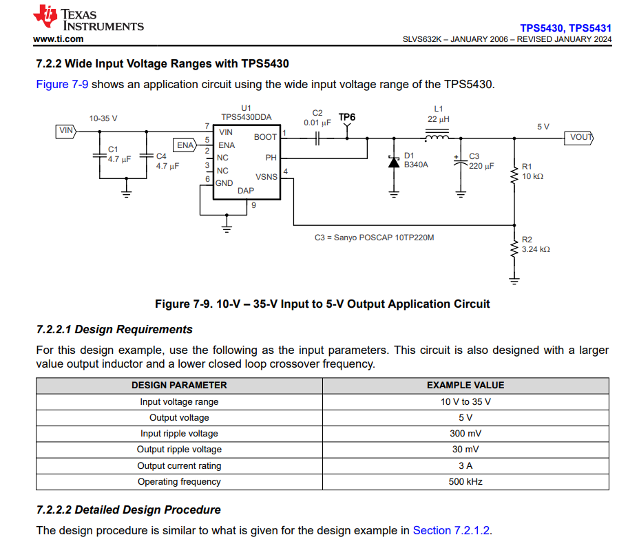
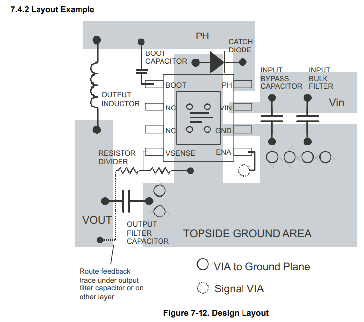
Power supplies:
https://www.digikey.com/en/products/detail/texas-instruments/TPS5430DDA/968136
Higher Priority:
Higher Affects:
Lower Priority:
Lower Affects:
To move the design process along, I made the following assumptions:
Count the number of pins needed:
Total number of pins required:
Calculate the current output for each power supply:
Summary of calculated values:
| Vin | Vout | Iout | Pout | Regulator | Pdiss |
|---|---|---|---|---|---|
| 8-30V | +5V | 3A | 15W | Buck (90% eff) | 1.67W |
| 8-30V | +3V3 | 3A | 9.9W | Buck (90% eff) | 1.10W |
| +3V3 | +1V8 | 1A | 1.8W | LDO | 1.50W |
| +3V3 | +1V5 | 1A | 1.5W | LDO | 1.80W |
Maximum amount of input current would be around 5A for the lowest 8V input.
Inital package research:
Package analysis:
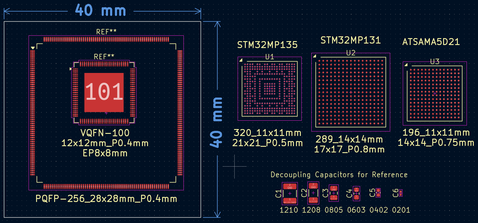
A few benefits include:
A few drawbacks include:
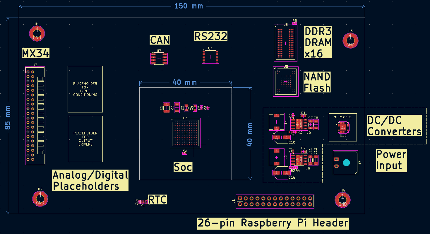
Right now, I'm thinking that the overall board size will be between 50x50mm and 100x100mm, and I'll keep that in mind when picking out the remaining components.
Next Steps: Focus on designing each 'section' of components, and then combining them on one board.
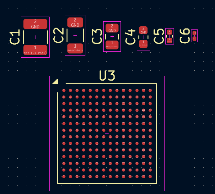
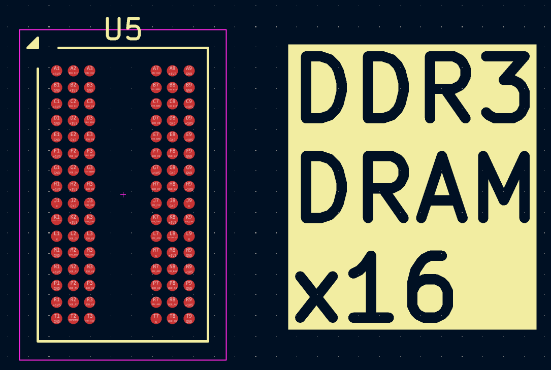
MT41K256M16TW 32M x 16-bit x 8 Banks (4-Gbit / 512 MB) DDR3L SDRAM, 1.35V nominal supply voltage, Rev. P, FBGA-96 (8x14mm) Package_BGA:Micron_FBGA-96_8x14mm_Layout9x16_P0.8mm
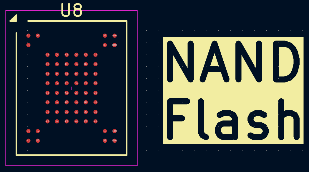
MT29F2G08ABDHC FLASH - NAND Memory IC 2Gbit Parallel 63-VFBGA (10.5x13) Package_BGA:BGA-63_9x11mm_Layout10x12_P0.8mm
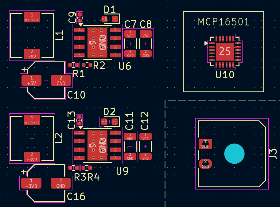
Referencing the table I made earlier, I would search both Digikey/Mouser and the SoC datasheet for appropriate power supplies. For this demo, I decided on the following:
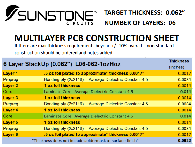
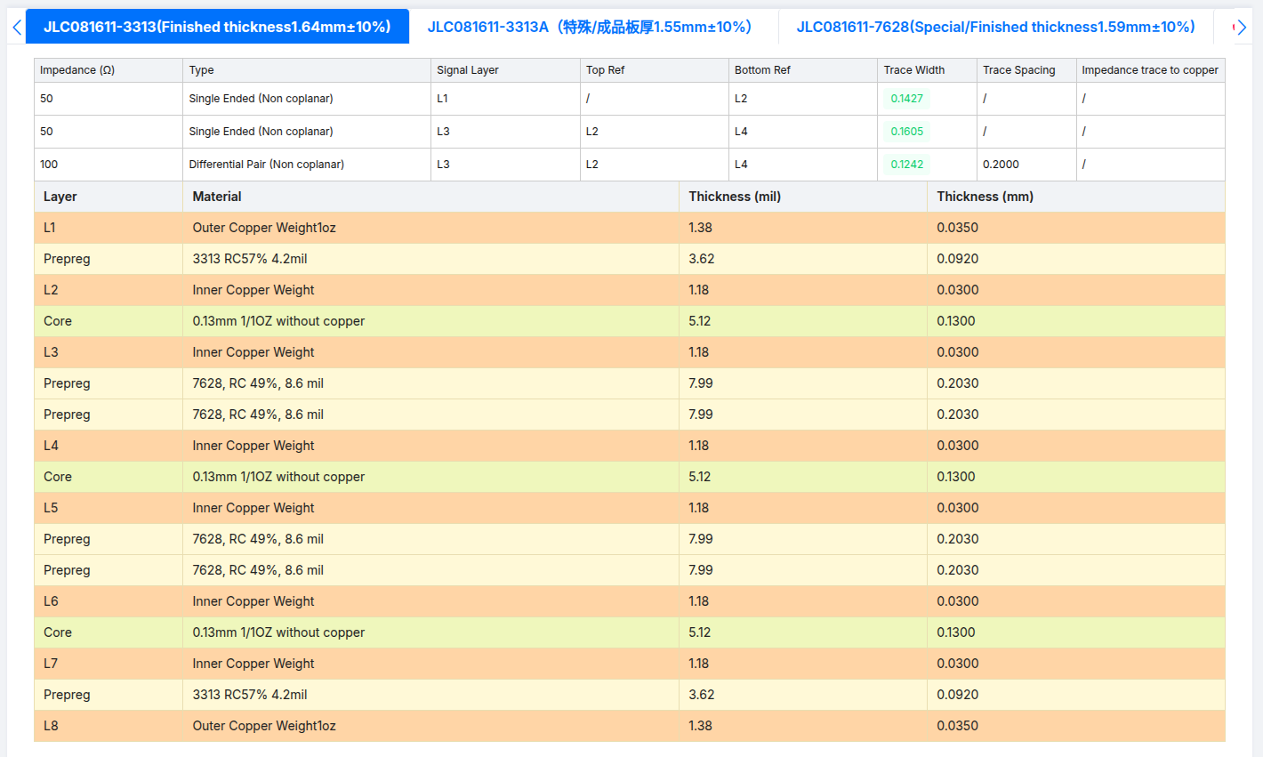
https://www.sunstone.com/docs/default-source/layer-stack-up-2022/l06-062-1-hv2.pdf
%% Standard trace width rules use 10 mils per amp for outer layers and 20 mils per amp for inner layers, assuming 1 oz copper. %%
However, I started calculating and the trace widths needed to be larger than what was possible, especially on the outer layers.
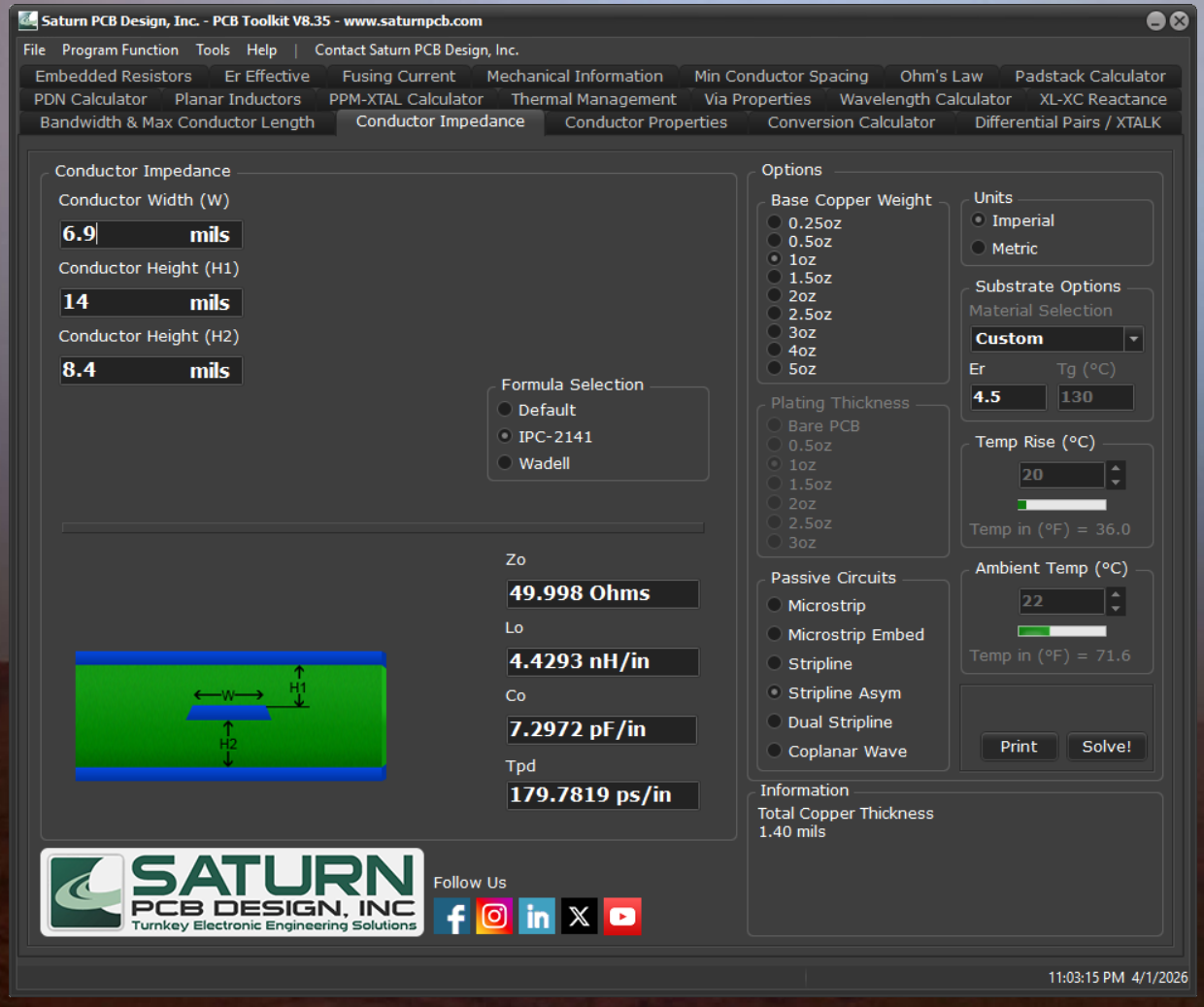
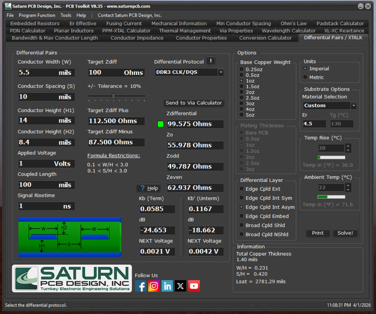
Even making the board thinner (1.0mm) and going up to 8 layers did not help routing DDR3 on the outer layers.
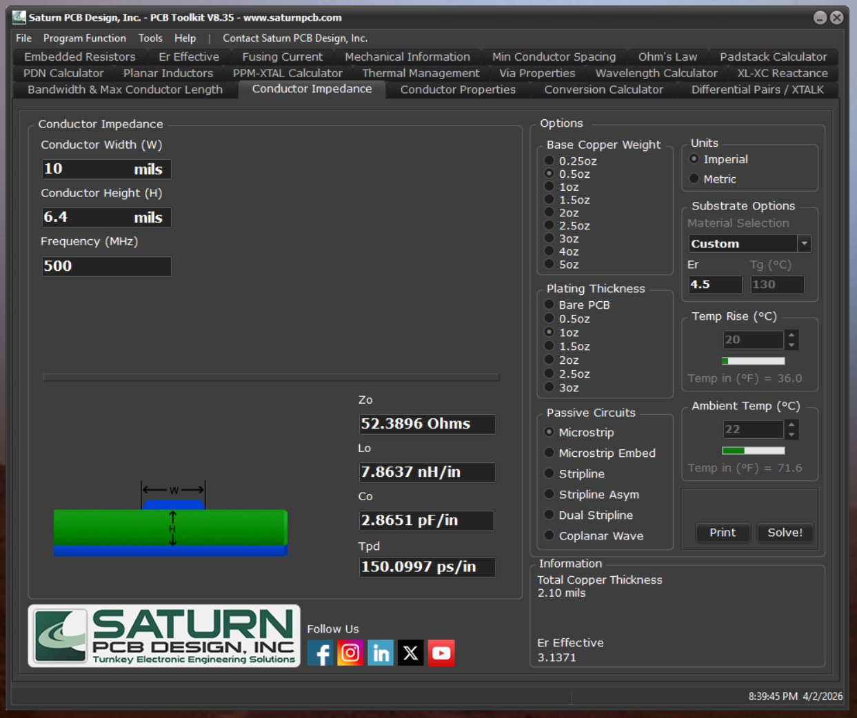
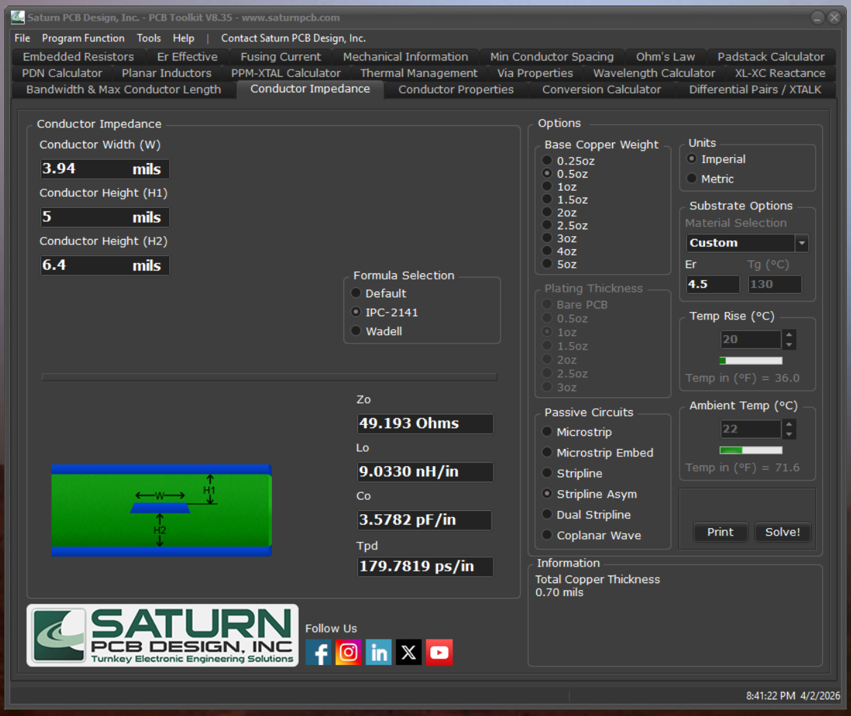
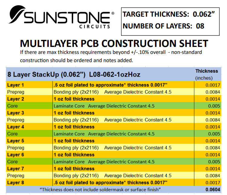
Moving to an 8-layer board has many benefits:
Drawbacks:
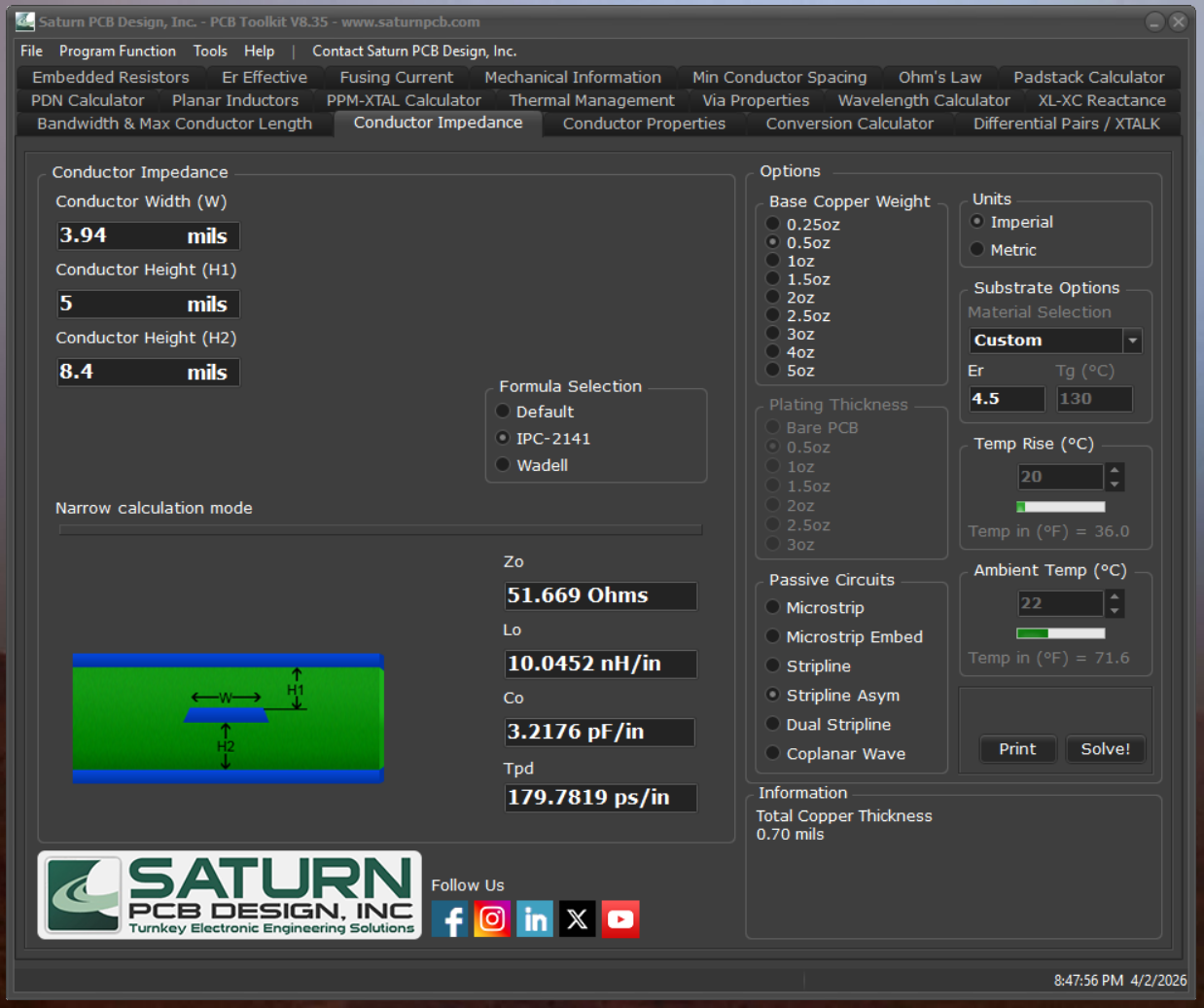
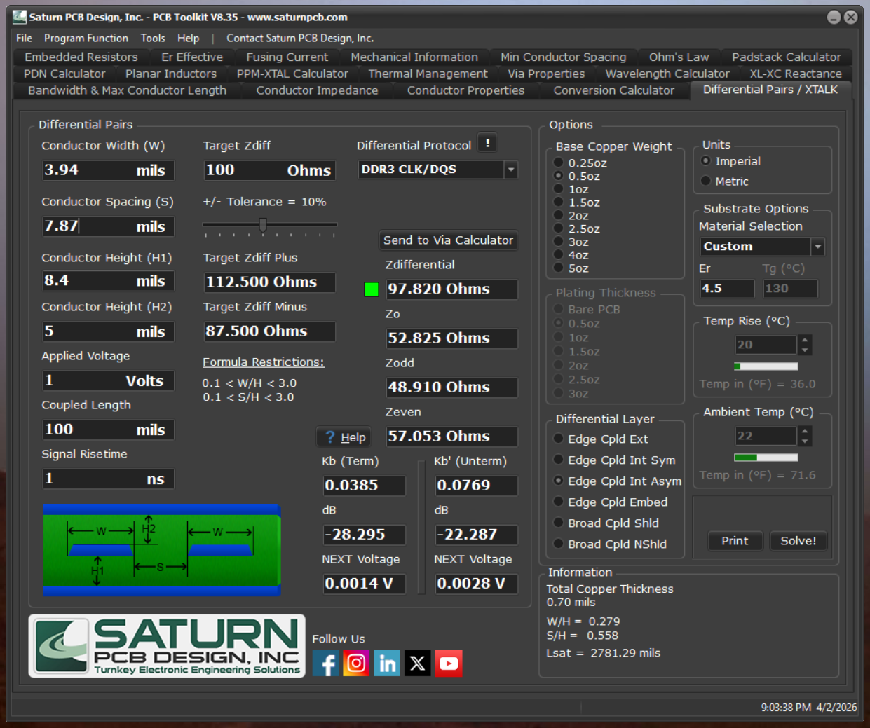
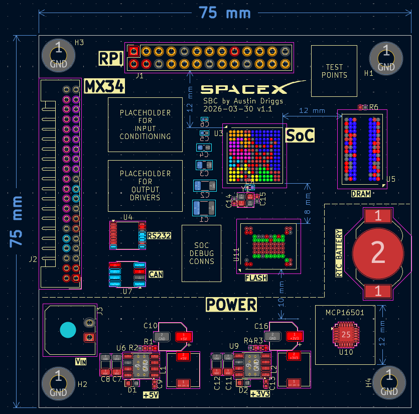
At this point, I would verify this layout and 3D model with any mechanical engineers.
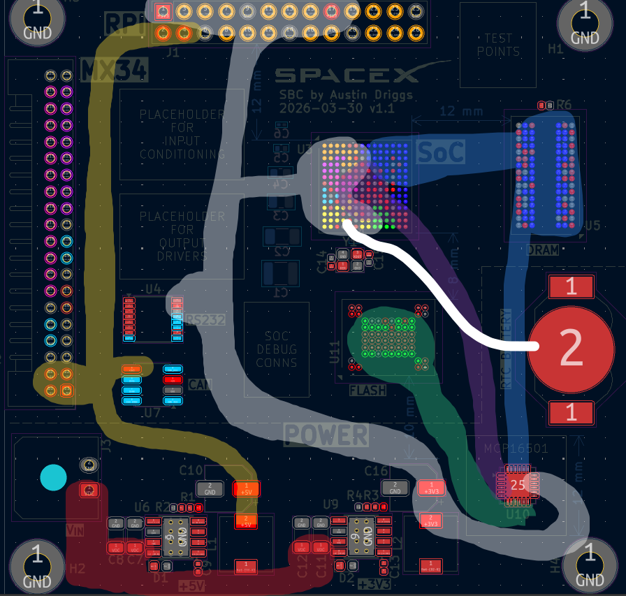
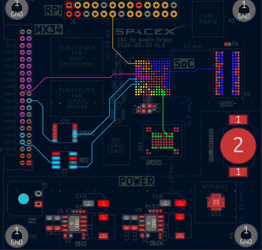
Inputs:
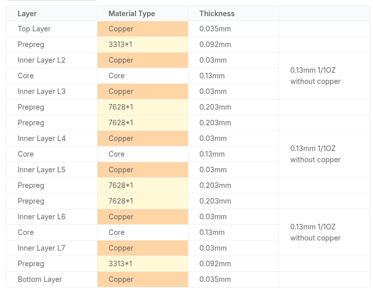
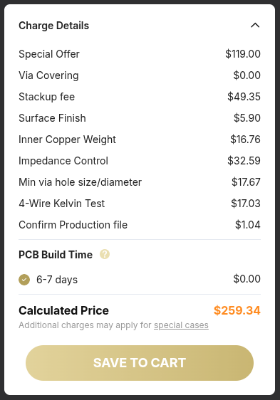
Total = $259.34 for 10 boards = $25.93 per board.
You are working with a design engineer on a small computer board.
The computer board has a SoC, DDR3 DRAM, NAND flash, DC input that is converted to 5V and 3.3V using an onboard DC/DC converter, I/O circuits, etc.
The SoC is available in BGA, QFN, QFP, bare die. The package outline varies between 8mm x 8mm to 40mm x 40mm depending on the ball/pin pitch which varies between 0.4mm to 1.0mm
The NAND flash is available in BGA, QFN, and QFP
The SoC consumes 5W, the DRAM 1W, the NAND flash 0.5W
You have to help the engineer define the board size, component placement, component selection because the components come in different sizes, footprints, etc, select the board stack up and board technology.
Started with asking questions, defining requirements, and establising assumptions.
Calculations for power, number of SoC pins, and trace impedance values.
Researched, analyzed, and selected a SoC package.
Selected SoC peripherals including the DRAM, Flash, and RTC.
Determined types and ratings for the voltage regulators.
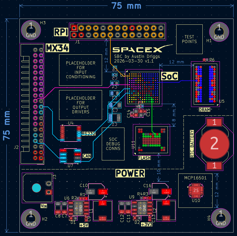
Designed the stackup, technology, and component placement.
| Qty | Value | Footprint | References |
|---|---|---|---|
| 6 | R_US | Resistor_SMD:R_0402_1005Metric | R1, R2, R3, R4, R5, R6 |
| 5 | C | Capacitor_SMD:C_1206_3216Metric | C2, C7, C8, C11, C12 |
| 4 | MountingHole_Pad | MountingHole:MountingHole_3.2mm_M3_Pad | H1, H2, H3, H4 |
| 3 | C | Capacitor_SMD:C_0402_1005Metric | C5, C9, C13 |
| 2 | 12pF | Capacitor_SMD:C_0402_1005Metric | C14, C15 |
| 2 | C_Polarized | Capacitor_SMD:CP_Elec_5x3 | C10, C16 |
| 2 | D_Schottky | Diode_SMD:D_0603_1608Metric | D1, D2 |
| 2 | L_Iron | Inductor_SMD:L_6.3x6.3_H3 | L1, L2 |
| 2 | TPS5430DDA | Package_SO:TI_SO-PowerPAD-8_ThermalVias | U6, U9 |
| 1 | 26PIN_RPI_HEADER | Connector_PinSocket_2.54mm:PinSocket_2x13_P2.54mm_Vertical | J1 |
| 1 | 8MHz | Crystal:Crystal_SMD_2520-4Pin_2.5x2.0mm | Y1 |
| 1 | ATSAMA5D21 | Package_BGA:Microchip_TFBGA-196_11x11mm_Layout14x14_P0.75mm_SMD | U3 |
| 1 | BatteryHolder_LINX_BAT-HLD-012-SMT | Battery:BatteryHolder_LINX_BAT-HLD-012-SMT | RTC BATTERY |
| 1 | C | Capacitor_SMD:C_0805_2012Metric | C3 |
| 1 | C | Capacitor_SMD:C_1210_3225Metric | C1 |
| 1 | C | Capacitor_SMD:C_0603_1608Metric | C4 |
| 1 | C | Capacitor_SMD:C_0201_0603Metric | C6 |
| 1 | Conn_01x02 | Connector_Molex:Molex_Micro-Fit_3.0_43650-0200_1x02_P3.00mm_Horizontal | J3 |
| 1 | MAX3221 | Package_SO:SSOP-16_4.4x5.2mm_P0.65mm | U4 |
| 1 | MCP16501TE-E/RMB | Package_DFN_QFN:QFN-24-1EP_4x4mm_P0.5mm_EP2.7x2.7mm | U10 |
| 1 | MCP2562-E-SN | Package_SO:SOIC-8_3.9x4.9mm_P1.27mm | U7 |
| 1 | MT40A512M16JY | Package_BGA:BGA-63_9x11mm_Layout10x12_P0.8mm | U11 |
| 1 | MT41K256M16TW | Package_BGA:Micron_FBGA-96_8x14mm_Layout9x16_P0.8mm | U5 |
| 1 | MX34 40-PIN | Connector_JAE:JAE_LY20-40P-DLT1_2x20_P2.00mm_Horizontal | J2 |
| 1 | STM32MP131AAEx | Package_BGA:LFBGA-289_14x14mm_Layout17x17_P0.8mm | U2 |
| 1 | STM32MP135AAFx | Package_BGA:ST_TFBGA-320_11x11mm_Layout21x21_P0.5mm | U1 |
The 45 most common of 46 parts.
austindriggs/urc-payload-pcb
All-purpose control and interface board designed to manage mission-critical sensors and electronics for University Rover Challenge at WVU.

MiroslavMitrovic/IgnitionController_STM32
Ignition controller implementation for 4T Single Cylinder/V-Twin motorcycle.

alvarop/chaac
This is a work in progress for a wireless weather station project.


brengi/CESE-PCB
Curso de Diseño de Circuitos Impresos de la Carrera de Especialización en Sistemas Embebidos

tuna-f1sh/whitterm-wt220
Design files, firmware and linux scripts for my /clever/ serial terminal, the Whitterm-220 - WT-220.

ApplePie420/OpenJBOD-CM4
This project is heavily inspired by the work of TheGuyDanish, specifically his OpenJBOD thingamajig.

It measures 75 × 75 mm and has 8 copper layers, 1.6 mm thick.
46 parts, built around the ATSAMA5D21C-CU, MAX3221CPW, TPS5430DDA and MCP16501TE-E/RMB. The full list of its parts is on this page, with links to each part's symbol and footprint where PCBKit's library has them.
From the austindriggs/spacex-sbc repository on GitHub, at the commit this page was made from: the board is spacex-sbc.kicad_pcb and its schematic analog.kicad_sch. PCBKit opens the board in the browser, with nothing to install.
Its repository states no licence, so its author keeps all rights: ask austindriggs before reusing the design.