4 layers98.6 × 92.1 mm

 aslak3/ICE40UPDevBoard10
A development board for iCE40UP5K FPGAs
ICE40UPDevBoard is an open-source printed circuit board by aslak3, from the aslak3/ICE40UPDevBoard repository on GitHub, published under the GPL-2.0 licence. It is a 4-layer board of 97.8 × 69.8 mm with 96 parts on 83 nets, routed with 734 tracks and 133 vias.
It is built around the ICE40UP5K-SG48ITR50, R-78B5.0-2.0 and ADV7123KSTZ140, with the N25Q032A13ESC40F, AT24CS64-SSHM-B and DS3231MZ+ among its other parts. Its parts include 32 capacitors, 31 resistors, 10 connectors, 8 ICs and 5 diodes. It belongs with the microcontroller boards and fPGA and programmable logic boards and the FPGA and CPLD boards of this library.


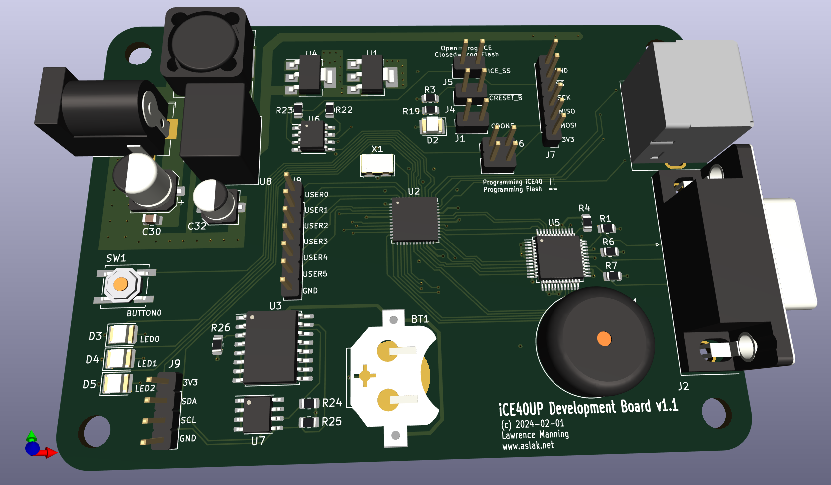
The specification for this development board is as follows:
A schematic is included here, along with the KiCAD data files, whcih are in KiCAD 6 format.
The PCB is a 4 layer board. My boards were manufactured by JLCPCB.
The jumper mechanism to route the SPI signals which carry the configuration data from the programmer was borrowed directly from the Lattice’s iCE40 UltraPlus Breakout Board.
Any iCE40 compatible programmer should be useable. I built my own, out of a Pi Pico, which is documented in another repo. The programmer has been used to program both the attached flash and the FPGA directly.
The design of this board is a very slightly tweaked version of the build I have on my bench. I have tweaked the LED and button connection after finding out that the three LED pins on the iCE40UP cannot source current for an LED and must sink it instead.
The following features have not been tested yet:
The best place to learn about this board is undoubtably my blog, including this post:
| Qty | Value | Footprint | References |
|---|---|---|---|
| 15 | 0.1u | Capacitor_SMD:C_0805_2012Metric | C2, C4, C6, C7, C9, C12, C13, C18, C20, C21, C22, C24, C25, C27, C28 |
| 9 | 4.7K | Resistor_SMD:R_0805_2012Metric | R8, R13, R14, R15, R16, R24, R25, R26, R30 |
| 5 | 10K | Resistor_SMD:R_0805_2012Metric | R3, R20, R21, R22, R23 |
| 5 | 10n | Capacitor_SMD:C_0805_2012Metric | C5, C8, C14, C15, C26 |
| 5 | 1K | Resistor_SMD:R_0805_2012Metric | R19, R27, R28, R29, R32 |
| 4 | 120 | Resistor_SMD:R_0805_2012Metric | R11, R12, R17, R18 |
| 4 | CDONE_LED | LED_SMD:LED_1210_3225Metric | D2, D3, D4, D5 |
| 4 | HOLE | MountingHole:MountingHole_4.3mm_M4 | H1, H2, H3, H4 |
| 3 | 10u | Capacitor_SMD:C_0805_2012Metric | C10, C16, C30 |
| 3 | 10u | Capacitor_Tantalum_SMD:CP_EIA-3216-10_Kemet-I | C1, C3, C19 |
| 3 | 75 | Resistor_SMD:R_0805_2012Metric | R1, R6, R7 |
| 3 | Conn_02x01 | Connector_PinHeader_2.54mm:PinHeader_2x01_P2.54mm_Vertical | J1, J4, J5 |
| 2 | 100 | Resistor_SMD:R_0805_2012Metric | R2, R5 |
| 2 | 100n | Capacitor_SMD:C_0805_2012Metric | C11, C23 |
| 2 | 47 | Resistor_SMD:R_0805_2012Metric | R9, R10 |
| 1 | 10u | Capacitor_SMD:CP_Elec_5x5.7 | C32 |
| 1 | 10u | Inductor_SMD:L_12x12mm_H4.5mm | L1 |
| 1 | 4.7u | Capacitor_SMD:C_0805_2012Metric | C31 |
| 1 | 470u | Capacitor_SMD:CP_Elec_6.3x7.7 | C29 |
| 1 | 47u | Capacitor_Tantalum_SMD:CP_EIA-7343-15_Kemet-W | C17 |
| 1 | 530 | Resistor_SMD:R_0805_2012Metric | R4 |
| 1 | ADV7123KSTZ140 | Package_QFP:LQFP-48_7x7mm_P0.5mm | U5 |
| 1 | AT24CS64-SSHM | Package_SO:SOIC-8_3.9x4.9mm_P1.27mm | U7 |
| 1 | AZ1117-1.2 | Package_TO_SOT_SMD:SOT-223-3_TabPin2 | U1 |
| 1 | AZ1117-3.3 | Package_TO_SOT_SMD:SOT-223-3_TabPin2 | U4 |
| 1 | BUZZER | Buzzer_Beeper:Buzzer_15x7.5RM7.6 | SP1 |
| 1 | Battery_Cell | Battery:BatteryHolder_Keystone_3000_1x12mm | BT1 |
| 1 | Bead | Inductor_SMD:L_1206_3216Metric | FB1 |
| 1 | Conn_01x04 | Connector_PinHeader_2.54mm:PinHeader_1x04_P2.54mm_Vertical | J9 |
| 1 | Conn_01x06 | Connector_PinHeader_2.54mm:PinHeader_1x06_P2.54mm_Vertical | J7 |
| 1 | Conn_01x07 | Connector_PinHeader_2.54mm:PinHeader_1x07_P2.54mm_Vertical | J8 |
| 1 | Conn_02x02_Odd_Even | Connector_PinHeader_2.54mm:PinHeader_2x02_P2.54mm_Vertical | J6 |
| 1 | DB15HD_FEMALE_SVGA | Connector_Dsub:DSUB-15-HD_Female_Horizontal_P2.29x1.98mm_EdgePinOffset3.03mm_Housed_MountingHolesOffset4.94mm | J2 |
| 1 | DS3231M | Package_SO:SOIC-16W_7.5x10.3mm_P1.27mm | U3 |
| 1 | ICE40UP5K-SG48ITR | Package_DFN_QFN:QFN-48-1EP_7x7mm_P0.5mm_EP5.6x5.6mm | U2 |
| 1 | MBR130 | Diode_SMD:D_SOD-123 | D1 |
| 1 | MPUOSC | Oscillator:Oscillator_SMD_SeikoEpson_SG8002LB-4Pin_5.0x3.2mm | X1 |
| 1 | Mini-DIN-6 | aslakfp:Connector_Mini-DIN_Female_6Pin_2rows | J3 |
| 1 | N25Q032A13ESC40F | Package_SO:SOP-8_3.9x4.9mm_P1.27mm | U6 |
| 1 | POWERLJACK | Connector_BarrelJack:BarrelJack_Horizontal | CON2 |
| 1 | R-78B5.0-2.0 | Converter_DCDC:Converter_DCDC_RECOM_R-78E-0.5_THT | U8 |
| 1 | RESETBUTTON | Button_Switch_SMD:SW_Push_1P1T_NO_CK_KSC6xxJ | SW1 |
It measures 97.8 × 69.8 mm and has 4 copper layers, 1.6 mm thick.
96 parts, built around the ICE40UP5K-SG48ITR50, R-78B5.0-2.0, ADV7123KSTZ140 and N25Q032A13ESC40F. The full list of its parts is on this page, with links to each part's symbol and footprint where PCBKit's library has them.
From the aslak3/ICE40UPDevBoard repository on GitHub, at the commit this page was made from: the board is ICE40UPDevBoard.kicad_pcb and its schematic ICE40UPDevBoard.kicad_sch. PCBKit opens the board in the browser, with nothing to install.
Its repository publishes it under the GPL-2.0 licence: you may reuse it on that licence's terms (keep the author's notice, and for a copyleft licence share your changes alike).


asinghani/ibm-5151-controller
Building a VT100 emulator out of an IBM 5151 monitor and an FPGA


electronut/ElectronutLabs-hackaBLE
A tiny Nordic nRF52832 based board you can embed in your BLE projects.