Skip to the content
PCBKitNew board
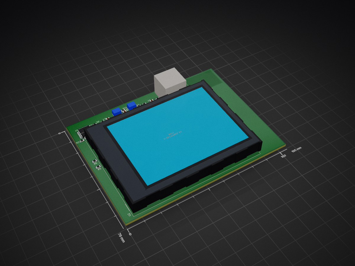
2 layers105 × 79 mmWaveform gen, the printed circuit board in 3D

A custom function generator designed using STM32F103, KiCad, and LTspice. The project implements a complete analog signal conditioning chain with adjustable gain, DC offset control, output buffering, and protection…

Size
105 × 79 mm
Copper layers
2
Thickness
1.6 mm
Parts
29
Nets
86
Pads
172
Tracks, vias
200, 16
Pours
1
Routed
Yes
KiCad
KiCad 10.0 (file 20260206)
Created
9 Jul 2026
Updated
9 Jul 2026

Overview

Waveform gen is an open-source printed circuit board by Aryan-Kodan, from the Aryan-Kodan/Function_generator repository on GitHub. It is a 2-layer board of 105 × 79 mm with 29 parts on 86 nets, routed with 200 tracks and 16 vias.

It is built around the LM358 and SMAJ24CA. Its parts include 10 resistors, 9 capacitors, 6 ICs, 1 diode and 1 connector. It belongs with the STM32 boards of this library.

Main components

2

README

README.md

STM32 Function Generator

A custom function generator designed using STM32F103, KiCad, and LTspice. The project implements a complete analog signal conditioning chain with adjustable gain, DC offset control, output buffering, and protection circuitry to generate clean analog waveforms suitable for laboratory and embedded applications.


Features

  • PWM-based waveform generation using STM32F103
  • Adjustable output amplitude
  • Adjustable DC offset
  • Low-pass reconstruction filter
  • Unity-gain buffer stage
  • Variable gain amplifier
  • Output driver for low-impedance loads
  • Output protection using TVS diode and series resistor
  • I²C TFT display interface
  • Custom PCB designed in KiCad
  • Complete circuit verification in LTspice

System Architecture

text
STM32 PWM Output
        │
        ▼
Reconstruction Filter
        │
        ▼
Buffer Amplifier
        │
        ▼
Variable Gain Stage
        │
        ▼
DC Offset Stage
        │
        ▼
Output Driver
        │
        ▼
Output Protection
        │
        ▼
BNC Output

Hardware

Microcontroller

  • STM32F103C8T6

Analog Front End

  • RC Reconstruction Filter
  • Buffer Amplifier
  • Variable Gain Amplifier
  • DC Offset Amplifier
  • Output Driver
  • Output Protection

Display

  • EA_eDIPTFT32-A TFT Display
  • I²C Interface

Software & Design Tools

  • KiCad 9
  • LTspice
  • STM32CubeIDE
  • Git
  • GitHub

Simulation

The complete analog signal chain was verified in LTspice.

Simulation includes:

  • Waveform generation
  • Gain adjustment
  • DC offset control
  • Frequency response
  • Output buffering
  • Output protection

PCB Design

The PCB was designed in KiCad featuring:

  • Two-layer PCB
  • Ground plane
  • Compact analog signal routing
  • STM32F103 integration
  • TFT display interface
  • BNC output connector

Repository Structure

text
STM32-Function-Generator/
│
├── BOM/
│   ├── Waveform_gen.csv
│
├── Images/
│   ├── KiCad/
│   │   ├── PCB.png
│   │   ├── PCB_3D.png
│   │   ├── PCB_through.png
│   │   └── Schematic.png
│   ├── LTspice/
│   │   ├── DC_offset_neg.png
│   │   ├── DC_offset_pos.png
│   │   ├── Max_amplitude.png
│   │   └── Unity_gain.png
│
├── KiCad/
│   ├── Waveform_gen.kicad_pcb
│   ├── Waveform_gen.kicad_pro
│   ├── Waveform_gen.kicad_sch
│
├── LTspice/
│   ├── Waveform_ge.asc
└── README.md

Project Workflow

  1. Waveform generation
  2. Reconstruction filtering
  3. Signal buffering
  4. Variable gain amplification
  5. DC offset adjustment
  6. Output buffering
  7. Output protection
  8. PCB implementation
  9. System verification

Key Specifications

ParameterValue
MCUSTM32F103C8T6
DisplayEA_eDIPTFT32-A
Output WaveformsSine, Square, Triangle (PWM Generated)
GainAdjustable
DC OffsetAdjustable
Output ProtectionTVS + Series Resistor
PCBTwo Layer
Design SoftwareKiCad
SimulationLTspice

Future Improvements

  • External DAC for improved waveform quality
  • Rotary encoder interface
  • Frequency sweep functionality
  • USB communication
  • Arbitrary waveform generation
  • Multiple output ranges
  • Amplitude calibration
  • FFT mode

Author

Aryan Kodan

GitHub: https://github.com/Aryan-Kodan


License

This project is released under the MIT License.

Parts

29
QtyValueFootprintReferences
8100nCapacitor_SMD:C_0805_2012MetricC3, C4, C5, C6, C7, C8, C9, C10
610kResistor_SMD:R_0805_2012MetricR3, R4, R8, R9, R10, R11
4LM358Package_SO:SOIC-8_3.9x4.9mm_P1.27mmU3, U4, U5, U6
24.7kResistor_SMD:R_0805_2012MetricR5, R6
11.6kResistor_SMD:R_0805_2012MetricR7
110kPotentiometer_SMD:Potentiometer_Bourns_3214W_VerticalRV2
11nCapacitor_SMD:C_0805_2012MetricC1
130kPotentiometer_SMD:Potentiometer_Bourns_3214W_VerticalRV1
150Resistor_SMD:R_0805_2012MetricR12
1Conn_CoaxialConnector_Coaxial:BNC_Amphenol_031-6575_HorizontalJ1
1EA_eDIPTFT32-ADisplay:EA_eDIPTFT32-XXXU2
1SMAJ24CADiode_SMD:D_SMAD1
1STM32F103C8TxPackage_QFP:LQFP-48_7x7mm_P0.5mmU1

Questions

How big is the Waveform gen PCB?

It measures 105 × 79 mm and has 2 copper layers, 1.6 mm thick.

What parts does the Waveform gen use?

29 parts, built around the LM358 and SMAJ24CA. The full list of its parts is on this page, with links to each part's symbol and footprint where PCBKit's library has them.

Where can I download the Waveform gen KiCad files?

From the Aryan-Kodan/Function_generator repository on GitHub, at the commit this page was made from: the board is KiCad/Waveform_gen.kicad_pcb and its schematic KiCad/Waveform_gen.kicad_sch. PCBKit opens the board in the browser, with nothing to install.

Can I use the Waveform gen design in my own project?

Its repository states no licence, so its author keeps all rights: ask Aryan-Kodan before reusing the design.

Similar boards

  • 2 layers103 × 95 mmDSO, the printed circuit board in 3D

    DSO

    Aryan-Kodan/Two_Channel_DSO

    A custom Multi-Channel Digital Storage Oscilloscope (DSO) designed using the STM32F103C8T6 microcontroller. This project combines a custom analog front-end, trigger circuitry, anti-alias filtering, multi-channel…
    94 parts
  • 2 layers132 × 59 mmWLC TX15W C1 V1.1, the printed circuit board in 3D

    WLC TX15W C1 V1.1

    dvhai08/WLC_TX15W_C1

    Wireless Charging (WLC) MP A11 Power Transmitter

    127 parts
  • 2 layers100 × 47.5 mmController, the printed circuit board in 3D

    Controller

    DLaxV-Community-Projects-Hub/Open-Shot-Clock

    Build your own DIY Shot Clock

    175 parts5CERN-OHL-P-2.0
  • 4 layers55 × 55 mmCaw bms, the printed circuit board in 3D

    Caw bms

    noxrick91/caw-bms

    锂电池管理系统

    154 parts228GPL-3.0
  • 2 layers34 × 96 mmGem solder, the printed circuit board in 3D

    Gem solder

    arlenko/gem-solder

    💎 DIY soldering iron controller

    114 parts12CERN-OHL-S-2.0
  • 6 layers158 × 174 mmTritonECU Main, the printed circuit board in 3D

    TritonECU Main

    alpauna/TritonECU

    ESP32-S3 engine control unit — fuel injection, ignition timing, wideband O2 (CJ125/LSU 4.9), dashboard, and MQTT telemetry

    457 parts10
  • 4 layers84 × 55 mmGrblPANEL, the printed circuit board in 3D

    GrblPANEL

    dresco/grblpanel_main_board

    KiCad implementation of a grblPANEL control board

    143 parts2
  • 2 layers88.8 × 76 mmArch Bridge, the printed circuit board in 3D

    Arch Bridge

    SeraphimlabsLLC/Arch_Bridge

    DCC-EX to Loconet accessory bus interface

    102 parts2AGPL-3.0