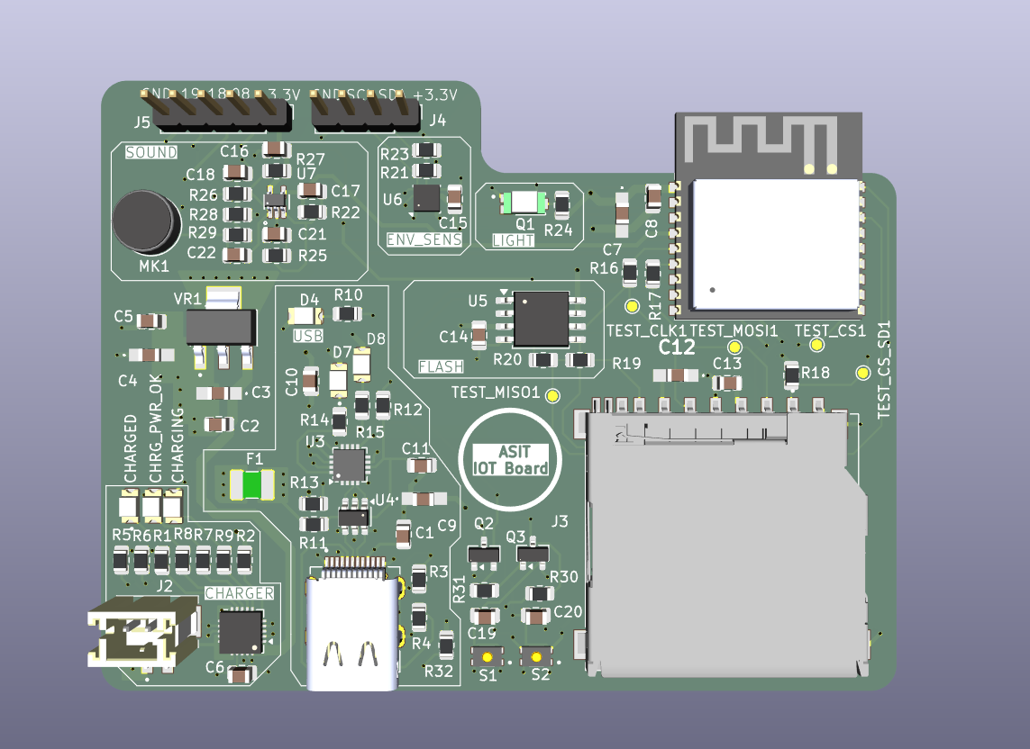
IOT is an open-source printed circuit board by aryan-asit, from the aryan-asit/Telemetry-iot-project repository on GitHub. It is a 4-layer board of 77.5 × 59.5 mm with 85 parts on 76 nets, routed with 670 tracks and 150 vias.
It is built around the ESP32-C3-WROOM-02-H4, BME280 and MAX4466EXK+T, with the W25Q32JVSSIQ, GSD090012SEU and TEMT6000X01 among its other parts. Its parts include 32 resistors, 22 capacitors, 7 ICs, 5 connectors and 3 transistors. It belongs with the home automation and IoT boards and the ESP32 and RISC-V boards of this library.
A custom 4-layer IoT Telemetry Board designed from scratch using KiCad. The board is built around an ESP32 and integrates environmental sensing, local data storage, USB connectivity, wireless communication, and battery charging and power management in a compact PCB.
Project Overview
The goal of this project was to design a compact and reliable IoT hardware platform capable of collecting environmental data, processing it locally, storing telemetry data, and communicating wirelessly.
The project covers the complete PCB development workflow, from component selection and schematic design to PCB layout, verification, 3D inspection, and manufacturing file generation.
3D PCB View
Key Features
ESP32 Processing and Connectivity
The ESP32 is the main controller of the board and provides:
Sensor data acquisition
Local data processing
Wi-Fi connectivity
Bluetooth connectivity
Communication with external peripherals
Sensors
The board includes multiple sensing elements for environmental and acoustic monitoring:
Microphone for sound sensing
Humidity sensor for environmental monitoring
Ambient light sensor for light-level measurement
Data Storage
Two storage options are integrated into the board:
Micro SD card for removable and higher-capacity data storage
Flash memory for local non-volatile storage
Power Management
The power section is based on the MCP73871 battery charging and power-management IC.
Main power features include:
USB Type-C power input
Battery charging
Power-path management
Battery-powered operation
Dedicated 3.3 V regulation using an LM1117-3.3V regulator
USB Type-C
A USB Type-C connector is included for power input and USB communication.
PCB Stack-Up
The board uses a 4-layer PCB stack-up to improve power distribution, grounding, and routing flexibility.
Layer
Purpose
Layer 1
Signal
Layer 2
Ground Plane
Layer 3
Power Plane - 5 V and 3.3 V zones
Layer 4
Signal
The dedicated ground and power layers provide continuous return paths and simplify power distribution across the board.
Communication Interfaces
Interface
Purpose
I2C
Sensor and peripheral communication
SPI
SD card, flash memory, and other peripherals
USB
Power, programming, and communication
Wi-Fi
Wireless connectivity
Bluetooth
Short-range wireless connectivity
System Architecture
text
                         +---------------------+
                         |     USB Type-C      |
                         |    Power / USB      |
                         +----------+----------+
                                    |
                                    v
                         +---------------------+
                         |      MCP73871       |
                         | Battery Charging &  |
                         |   Power Management  |
                         +----------+----------+
                                    |
                                    v
                         +---------------------+
                         |     LM1117-3.3V     |
                         |  Voltage Regulation |
                         +----------+----------+
                                    |
                                    v
                    +------------------------------+
                    |             ESP32            |
                    |      Processing & Control    |
                    |                              |
                    |       Wi-Fi + Bluetooth     |
PCB Design Workflow
1. Concept Development
Defined the requirements for a compact IoT telemetry platform covering sensing, processing, storage, communication, and power management.
2. Component Selection
Selected the ESP32, sensors, memory devices, charging IC, regulator, connectors, and supporting components based on the system requirements.
3. Schematic Design
Designed and reviewed the complete circuit schematic and connected the individual functional blocks.
4. Footprint Selection and Creation
Selected suitable KiCad footprints and created or customized footprints where required.
5. PCB Layout
Defined the 4-layer stack-up and placed components while considering board size, routing complexity, signal paths, power distribution, and component accessibility.
6. Routing
Routed signal, power, and communication connections with attention to return paths, grounding, and clean power distribution.
7. 3D Verification
Configured 3D models and inspected the complete board to verify component placement and the overall physical arrangement.
8. ERC and DRC Verification
Performed Electrical Rules Check (ERC) and Design Rules Check (DRC) to identify and resolve schematic and PCB design issues.
9. Manufacturing Output
Generated Gerber and other required manufacturing files for PCB fabrication.
Design Highlights
4-Layer PCB Design
The dedicated ground and power layers provide better power distribution and more flexible signal routing than a basic 2-layer approach.
Integrated Power Management
The MCP73871 handles battery charging and power-path management, while the LM1117-3.3V provides a regulated 3.3 V supply for the low-voltage circuitry.
Multiple Peripheral Interfaces
The board combines sensors, storage, USB, and wireless communication on a single PCB, making it suitable for different embedded and IoT applications.
Compact Functional Layout
The component placement and routing were optimized to balance board size, functionality, accessibility, and routing complexity.
The board can be adapted for applications such as:
Environmental monitoring
IoT sensor nodes
Wireless telemetry
Data logging
Noise monitoring
Ambient light monitoring
Smart embedded systems
Battery-powered IoT devices
Hardware prototyping
What I Learned
This project provided practical experience in:
4-layer PCB design
Schematic design and verification
Component selection
Footprint management
PCB placement and routing
Power distribution and grounding
Signal-integrity considerations
ERC and DRC debugging
3D PCB inspection
Gerber generation
Iterative hardware design and debugging
One of the main design challenges was finding the right balance between board size, routing complexity, power distribution, component placement, and overall functionality.
Future Improvements
Possible future improvements include:
Additional environmental sensors
Cloud-based telemetry
OTA firmware updates
Improved power optimization
Additional communication interfaces
Dedicated debugging and programming features
Enclosure and mechanical integration
Web or mobile dashboard for telemetry visualization
Author
Aryan Asit
B.Tech - Electronics and Communication Engineering
VLSI and Embedded Systems
Indian Institute of Information Technology Manipur
This is a learning recreation of the KLP-5e ESP32-C3 4-layer IoT sensor board. The PCB was recreated in KiCad by following the Tech Explorations tutorial, resulting in a design that closely matches the original.
A custom 4-layer IoT development board based on the ESP32-C3, featuring integrated LiPo battery management, a CP2102N USB-UART bridge, MicroSD support, and onboard environmental/audio sensors for embedded engineering…
4-layer ESP32-C3 based custom embedded IoT PCB featuring onboard temperature & humidity, light, and audio sensing, USB Type-C, Li-Po charging, and external flash memory.
A compact 4-layer IoT development board built around the ESP32-C3, integrating environmental sensing, local storage, USB-C power with LiPo battery management, and a programming/debug interface on a single board.
It measures 77.5 × 59.5 mm and has 4 copper layers, 1.6 mm thick.
What parts does the IOT use?
85 parts, built around the ESP32-C3-WROOM-02-H4, BME280, MAX4466EXK+T and W25Q32JVSSIQ. The full list of its parts is on this page, with links to each part's symbol and footprint where PCBKit's library has them.
Where can I download the IOT KiCad files?
From the aryan-asit/Telemetry-iot-project repository on GitHub, at the commit this page was made from: the board is IOT_PCB/IOT/IOT.kicad_pcb and its schematic IOT_PCB/IOT/ESP32-C3-02.kicad_sch. PCBKit opens the board in the browser, with nothing to install.
Can I use the IOT design in my own project?
Its repository states no licence, so its author keeps all rights: ask aryan-asit before reusing the design.