Skip to the content
PCBKitNew board
2 layers505.4 × 130.4 mmSplit keyboard, the printed circuit board in 3D

I decided to make a V2 which would allow me to redo/refine some features. That is I want to add a LiPo battery and change the requirement of having both sides plugged in separately to the PC. I already have the parts to build the keyboard so the grant is only for the PCB

Size
505.4 × 130.4 mm
Copper layers
2
Thickness
1.6 mm
Parts
262
Nets
171
Pads
1,096
Tracks, vias
1,507, 70
Pours
2
Routed
Yes
KiCad
KiCad 9.0 (file 20241229)
Created
10 Jan 2026
Updated
23 Mar 2026

Overview

Split keyboard is an open-source printed circuit board by Arwinplayz, from the Arwinplayz/Split-Keyboard-V2 repository on GitHub. It is a 2-layer board of 505.4 × 130.4 mm with 262 parts on 171 nets, routed with 1,507 tracks and 70 vias.

It is built around the S2B-PH-K-S(LF)(SN), PJ-320A and WS2812B-2020, with the MBR130T1G and NSMD050-33V among its other parts. Its parts include 117 diodes, 58 capacitors, 58 switches, 8 resistors and 4 ICs. It belongs with the keyboards and input and power boards and the nRF52 and nRF5x boards of this library.

Main components

5

README

README.md

Split-Keyboard V2

I recently got my PCB from JLCPCB but I realised that I had accidentally inverted the holes for the hotswap sockets. This makes it physically impossible for me to actually assembly it properly. Learning from my failures, I decided to make a V2 which would not only fix the socket problem but also allow me to redo/refine some features. That is I want to add a LiPo battery and change the requirement of having both sides plugged in separately to the PC. I already have the parts to build the keyboard so the grant is only for the PCB (and possibly extra stuff such as LiPo battery, resistors, JST PH connectors, etc)

Planning

I recently got my PCB from JLCPCB but I realised that I had accidentally inverted the holes for the hotswap sockets. This makes it physically impossible for me to actually assembly it properly. (Awkward placement + overlap with other components)
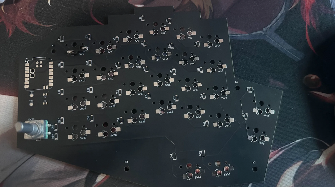
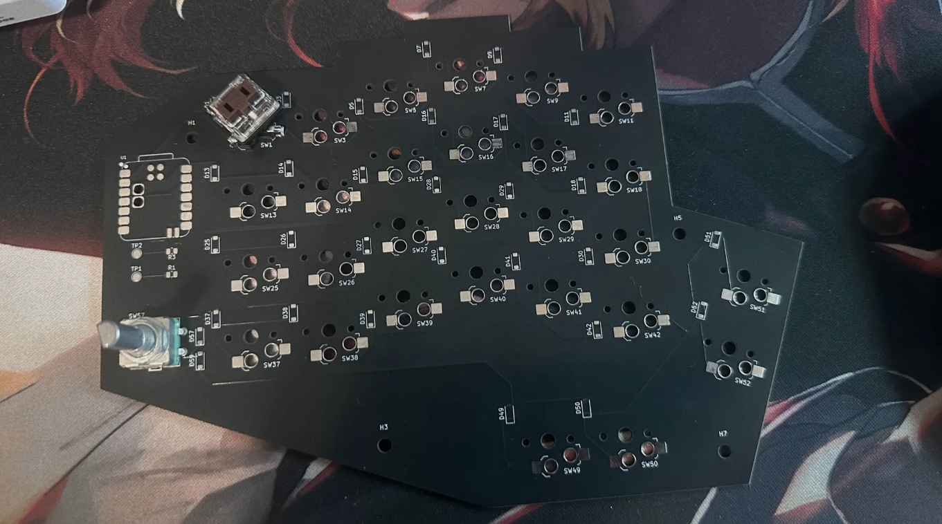
V1 PCB V1 PCB

Learning from my failures, I decided to make a V2 which would not only fix the socket problem but also allow me to redo/refine some features. That is I want to add a LiPo battery and change the requirement of having both sides plugged in separately to the PC. I already have the parts to build the keyboard so the grant is only for the PCB (and possibly extra stuff such as LiPo battery, resistors, JST PH connectors, etc)

GOALS:

Fix hotswap socket orientation Added better connectivity between the split keyboards (Master and Slave RP2040) Add support for 1s 3.4V LiPo Battery

Heavily Modified Schematic

So firstly, I realised that to use the master and slave approach, I needed a TRRS which connects the halves via UART. This meant that I needed a UARTTX, UARTRX but all my gpio pins were occupied. After some research I found that the nice!nano v2 was a good choice as it had the same Nordic chip. This allowed for bluetooth connection, a built in linear Li-Po charging circuit which helps avoid clutter. Furthermore, I added a 2 pin JST-PH connector for the Li-Po battery. There is also an RGB LED which will signal green for charged, yellow for 50$, red for low and blue for charging.
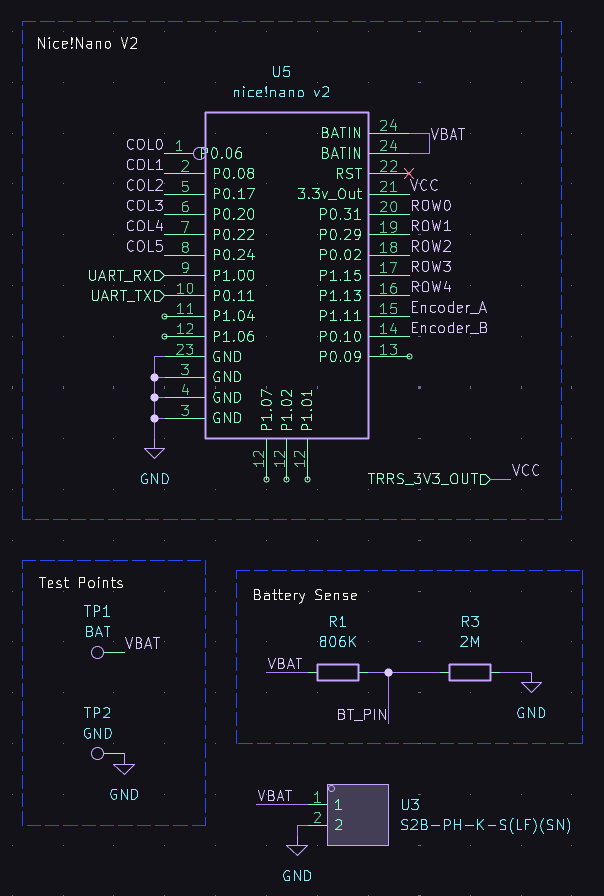
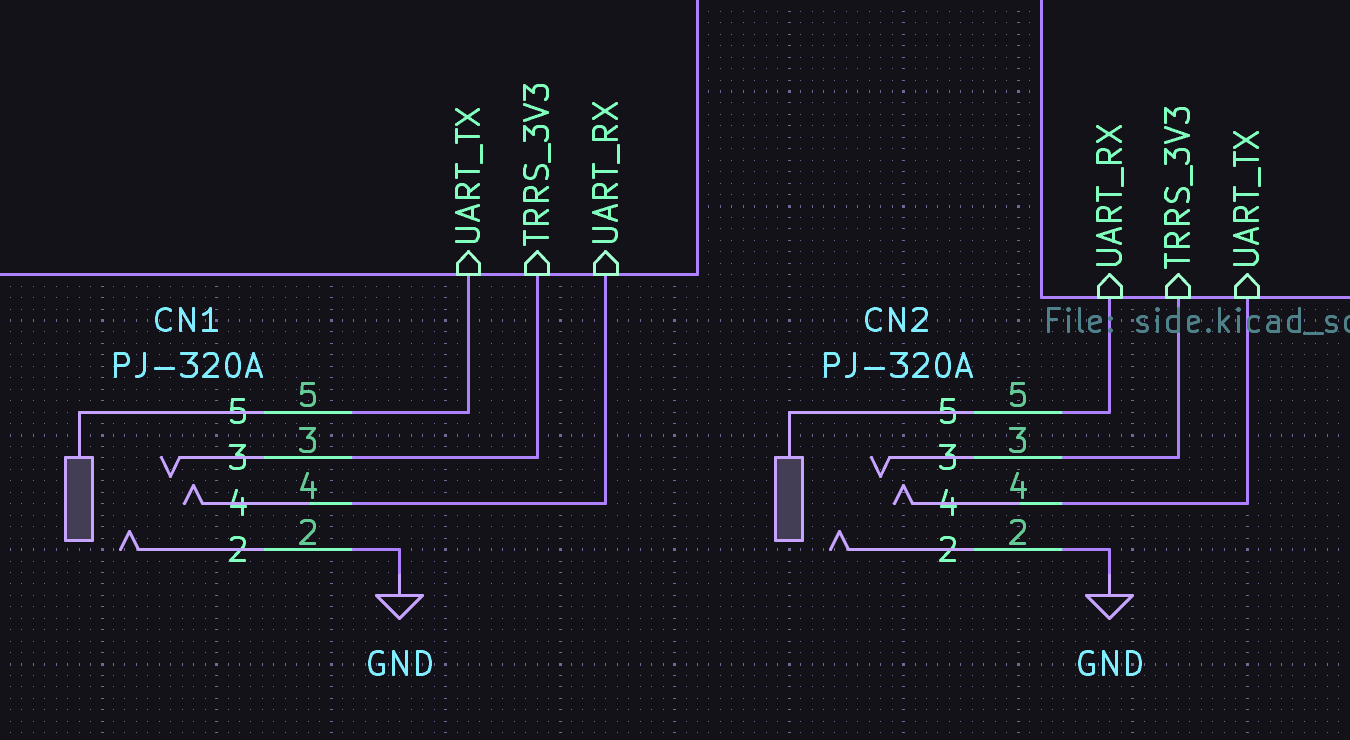
Nice!nano V2 TRRS LED

Routed half the PCB

So I managed to route half the PCB now. There were many problems related to footprints as the Nice!Nano doesn't really have a goof publicly available one and so I had to design it myself. Also I added LED lights for every switch and ensured the hotswap sockets were orientated the right way.
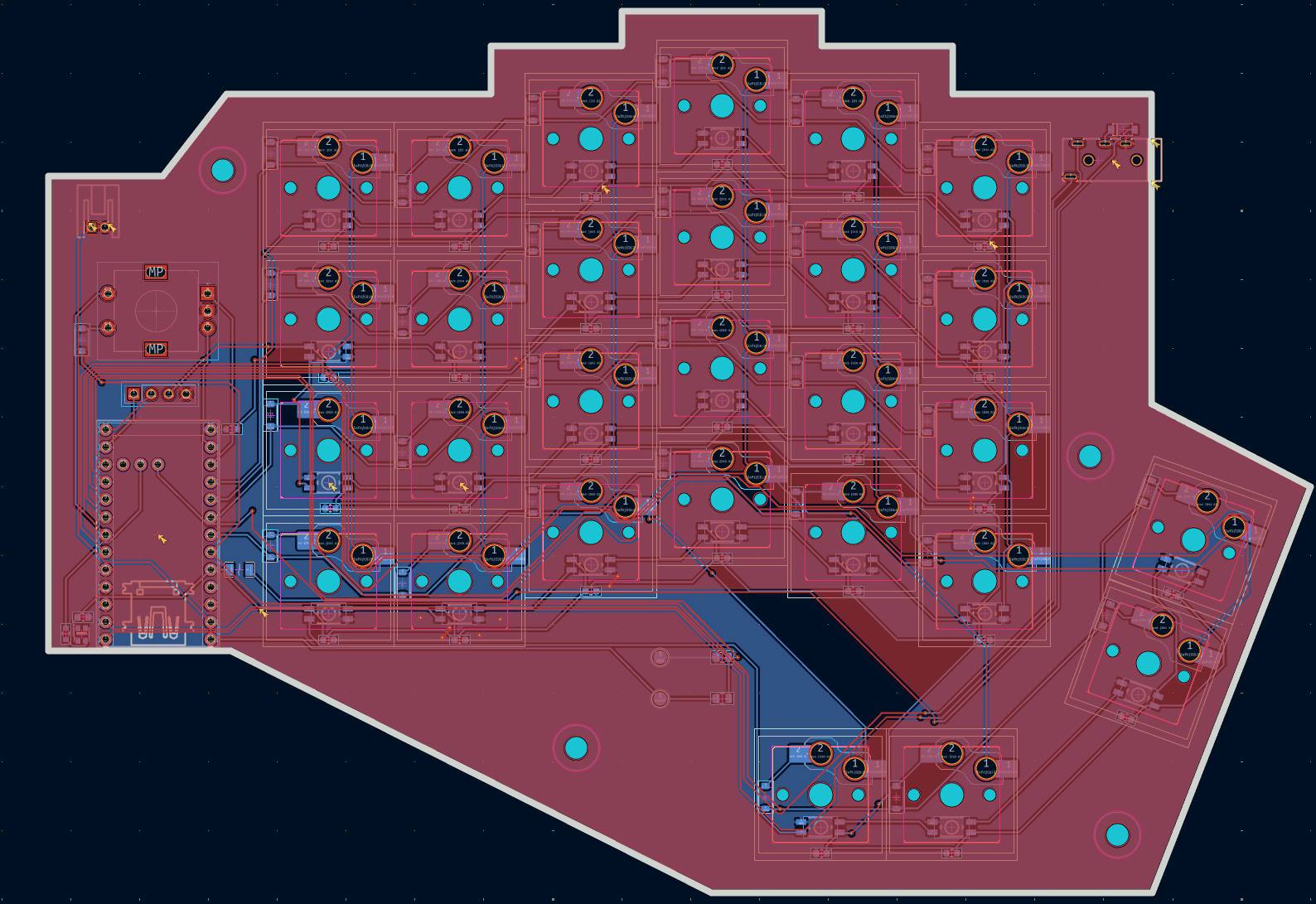
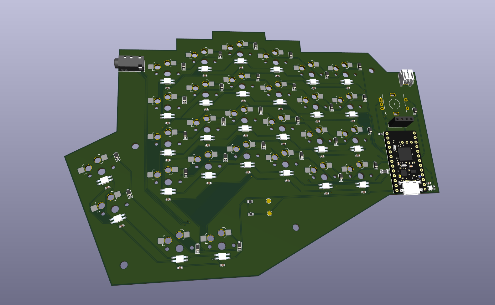
schematic 3d viewer

Finished Routing the PCB

So it took me a while to figure out how to mirror the left side. There was no easy way to do so I ended up flipping the edgecut and then redoing all the wiring. There is only 1 error on the ERC which is the left and right side aren't connected by this will get fixed with a TRRC cable.
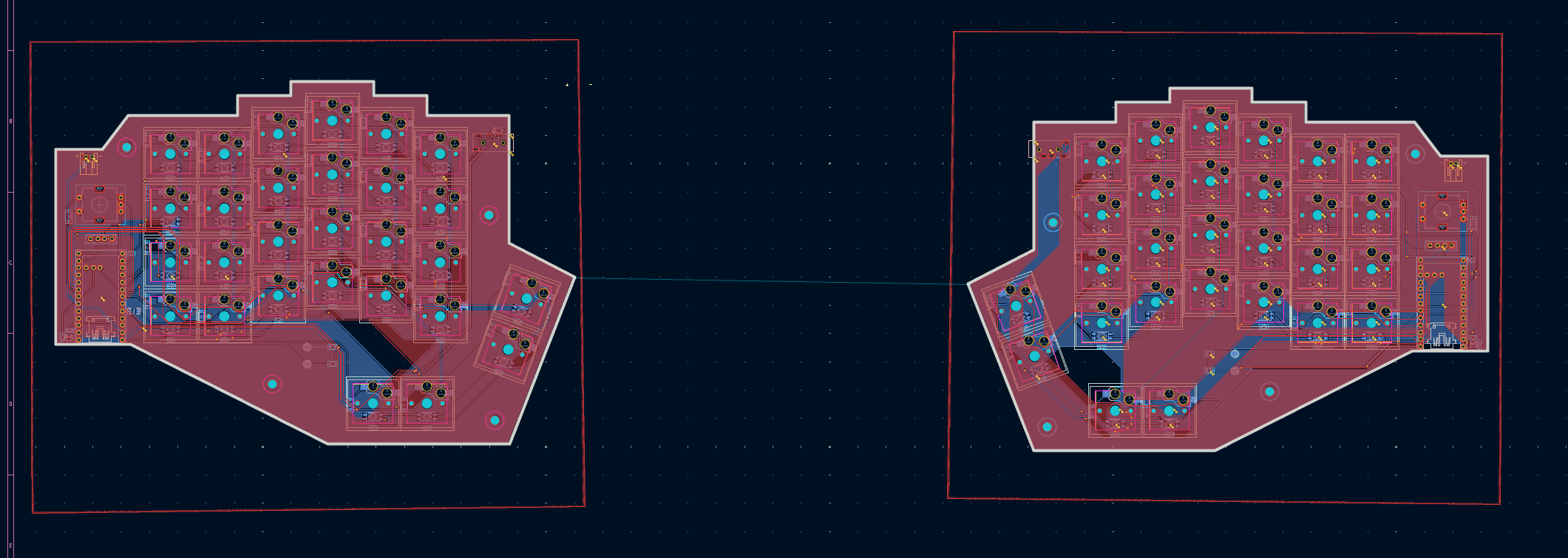
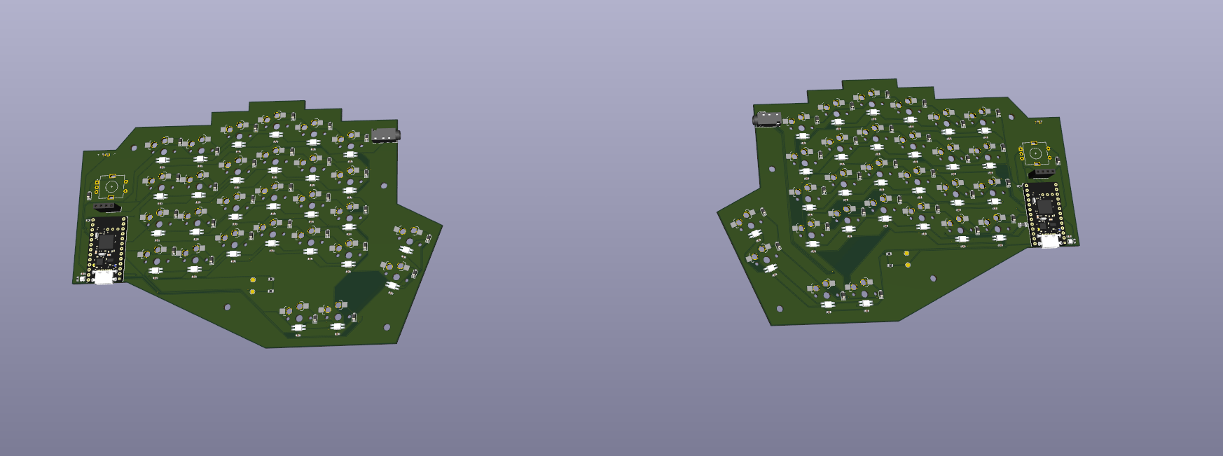
schematic 3d viewer

Gerber Files

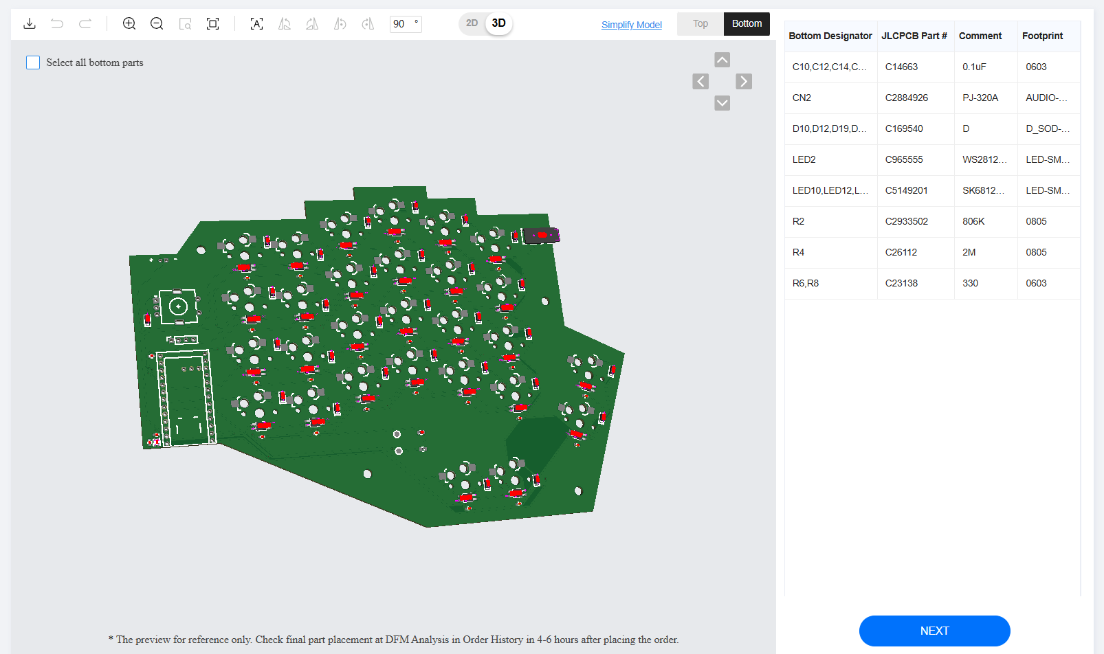
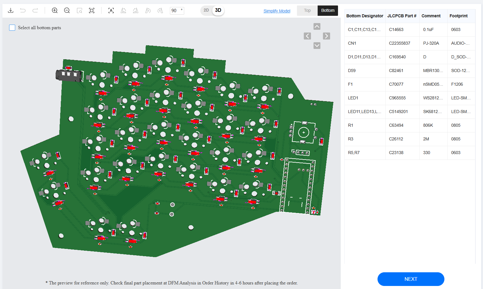
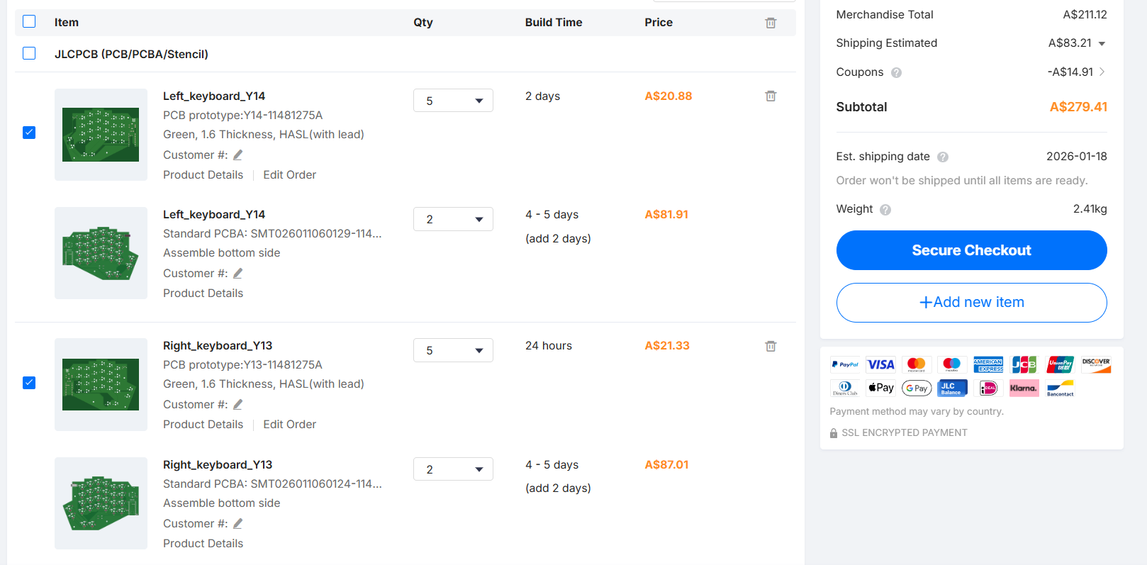
I decided to get PCBA due to the keybaord requiring several LED and Diodes which all require a certain orientation to work properly. A few components require PCBA to be placed. I do have 1 or 2 components which I will hand solder myself to help reduce the costs. The PCB was too large for PCBA so I have to order each half of the PCB seperately.
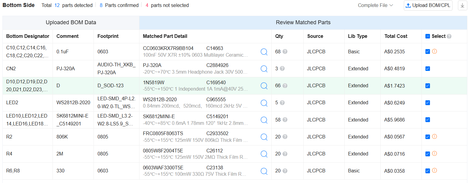
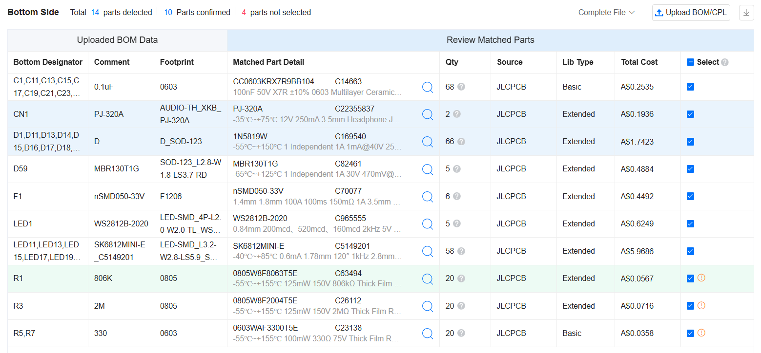
Left BOM RIght BOM Left 3D Right 3D total shipping

BOM

So since I already have most of the components such as rotary encoder, key switches, keycaps, etc, the BOM is prely for the parts I need for the PCB (the extra stuff that I didn't solder from JLC). So the total comes to about 227.98 USD. I really do not know how to make it cheaper as I've sourced everything from the cheapest sites I could find i.e aliexpress.
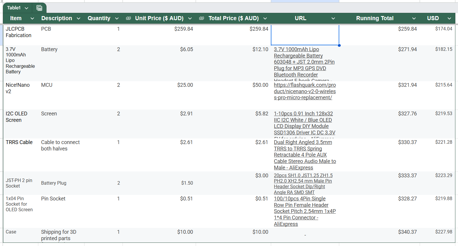
shipping

Parts

262
QtyValueFootprintReferences
580.1uFCapacitor_SMD:C_0603_1608MetricC1, C2, C10, C11, C12, C13, C14, C15, C16, C17, C18, C19, C20, C21, C22, C23 +42
58DDiode_SMD:D_SOD-123D1, D2, D10, D11, D12, D13, D14, D15, D16, D17, D18, D19, D20, D21, D22, D23 +42
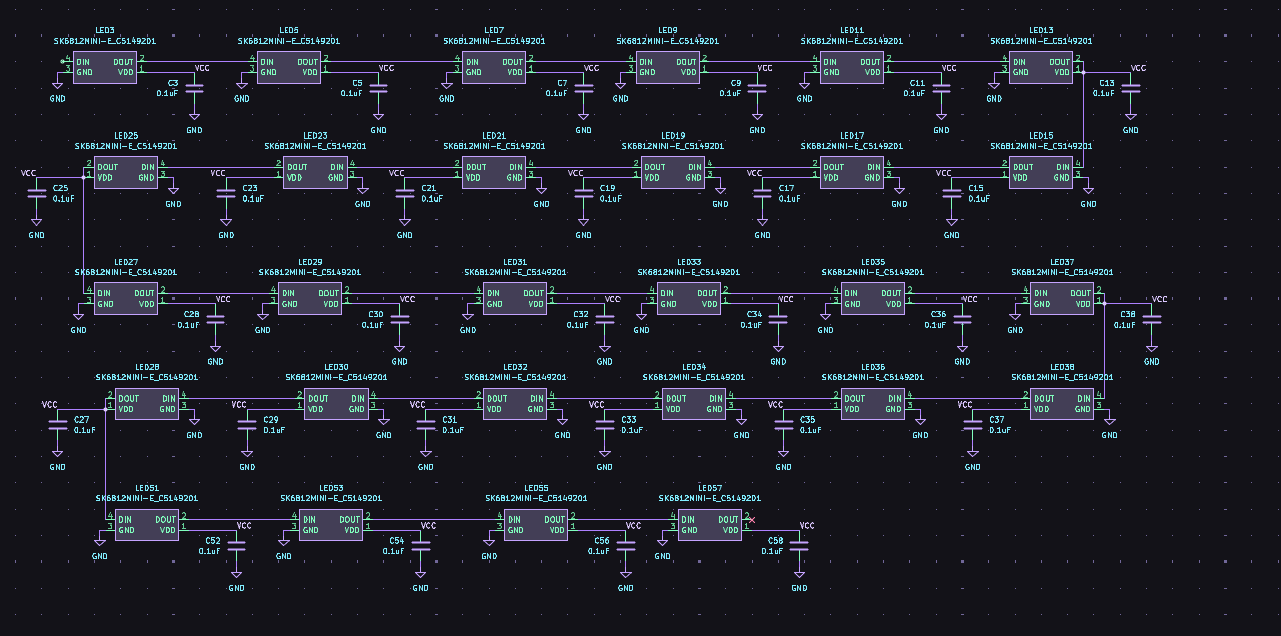
56SK6812MINI-E_C5149201lcsc:LED-SMD_L3.2-W2.8-LS5.9_SK6812MINI-ELED10, LED11, LED12, LED13, LED14, LED15, LED16, LED17, LED18, LED19, LED20, LED21, LED22, LED23, LED24, LED25 +40
56SW_Pushmarbastlib-choc:SW_choc_v1_HS_CPG135001S30_1uSW1, SW2, SW10, SW11, SW12, SW13, SW14, SW15, SW16, SW17, SW18, SW19, SW20, SW21, SW22, SW23 +40
8MountingHoleMountingHole:MountingHole_3.2mm_M3H1, H2, H3, H4, H5, H6, H7, H8
4330Resistor_SMD:R_0603_1608MetricR5, R6, R7, R8
22MResistor_SMD:R_0805_2012MetricR3, R4
2806KResistor_SMD:R_0805_2012MetricR1, R2
2BATTestPoint:TestPoint_Pad_D2.0mmTP1, TP3
2Conn_01x04_SocketConnector_PinSocket_2.54mm:PinSocket_1x04_P2.54mm_VerticalJ1, J2
2GNDTestPoint:TestPoint_Pad_D2.0mmTP2, TP4
2PJ-320Alcsc:AUDIO-TH_XKB_PJ-320ACN1, CN2
2RotaryEncoder_SwitchRotary_Encoder:RotaryEncoder_Alps_EC11E-Switch_Vertical_H20mmSW57, SW58
2S2B-PH-K-S(LF)(SN)lcsc:CONN-TH_S2B-PH-K-S-LF-SNU3, U4
2WS2812B-2020lcsc:LED-SMD_4P-L2.0-W2.0-TL_WS2812B-2020LED1, LED2
2nice!nano v2lcsc:NICE!NANO V2_2U5, U6
1MBR130T1Glcsc:SOD-123_L2.8-W1.8-LS3.7-RDD59
1nSMD050-33Vlcsc:F1206F1

Questions

How big is the Split keyboard PCB?

It measures 505.4 × 130.4 mm and has 2 copper layers, 1.6 mm thick.

What parts does the Split keyboard use?

262 parts, built around the S2B-PH-K-S(LF)(SN), PJ-320A, WS2812B-2020 and MBR130T1G. The full list of its parts is on this page, with links to each part's symbol and footprint where PCBKit's library has them.

Where can I download the Split keyboard KiCad files?

From the Arwinplayz/Split-Keyboard-V2 repository on GitHub, at the commit this page was made from: the board is PCB/Split keyboard.kicad_pcb and its schematic PCB/Split keyboard.kicad_sch. PCBKit opens the board in the browser, with nothing to install.

Can I use the Split keyboard design in my own project?

Its repository states no licence, so its author keeps all rights: ask Arwinplayz before reusing the design.

More from Arwinplayz/Split-Keyboard-V2

1
  • 2 layers183.2 × 128 mmRight keyboard, the printed circuit board in 3D

    Right keyboard

    Arwinplayz/Split-Keyboard-V2

    I decided to make a V2 which would allow me to redo/refine some features. That is I want to add a LiPo battery and change the requirement of having both sides plugged in separately to the PC.

    132 parts

Similar boards

  • 2 layers121.3 × 197.5 mmFlipdot, the printed circuit board in 3D

    Flipdot

    mitxela/flipdots

    KiCad designs and software for driving Hanover flipdot displays with a resolution of 13 by 28, as used in the FLIP fluid on Flipdots project

    521 parts10
  • 2 layers52 × 36 mmCyphalPicoBase CAN, the printed circuit board in 3D

    CyphalPicoBase CAN

    generationmake/CyphalPicoBase-CAN

    Board for the Raspberry Pi Pico to connect via CAN using OpenCyphal and UCANPHY Micro

    62 parts5CERN-OHL-W-2.0
  • 2 layers160 × 110 mmAcquedotto test v4 finale, the printed circuit board in 3D

    Acquedotto test v4 finale

    igorilla666/water-controller

    Scheda di controllo basata sul modulo Waveshare ESP32-S3-ETH, con ingressi sensore, RS-485, pilotaggio rele, buzzer e alimentazione/protezioni dedicate.

    139 parts1CERN-OHL-S-2.0
  • 4 layers90 × 160 mmTool power supply v1, the printed circuit board in 3D

    Tool power supply v1

    UBC-Hacker-Fab/tool-power-supply

    general power supply for tools

    125 parts1
  • 4 layers65 × 56 mmSensor HAT, the printed circuit board in 3D

    Sensor HAT

    Eniemooo/Sensor-HAT

    Open-hardware indoor air sensor (CO2, VOC/NOx, T/RH, light, sound): HAT for Raspberry Pi or standalone with Seeed XIAO + ESPHome. KiCad 10.

    112 parts
  • 4 layers26.7 × 55.2 mmSombrero MSX Goa'uld, the printed circuit board in 3D

    Sombrero MSX Goa'uld

    jabadiagm/MSXgoauldSD_tn20k

    MSX Goa'uld board with Tang Nano 20k and SD support

    17 parts41GPL-3.0
  • 2 layers60 × 110 mmAddaTone components, the printed circuit board in 3D

    AddaTone components

    dchwebb/Addatone

    Eurorack Additive Oscillator based on Lattice FPGA and ARM MCU

    95 parts13
  • 4 layers65 × 56.1 mmMhd314, the printed circuit board in 3D

    Mhd314

    yanava/mhd314

    mahaudio DAC for the RaspberryPi

    195 parts4BSD-3-Clause