4 layers50 × 37.5 mm
NRF9161-DEV BOARD
anand2532/nRF9161-DEV-BOARD
A small 50 × 37.5 mm LTE-M / NB-IoT + GNSS modem board built around the Nordic nRF9161. Any host MCU controls it with AT commands over one 10-pin UART header.
84 parts

 anand2532/nRF9161-DEV-BOARD
A small 50 × 37.5 mm LTE-M / NB-IoT + GNSS modem board built around the Nordic nRF9161. Any host MCU controls it with AT commands over one 10-pin UART header.
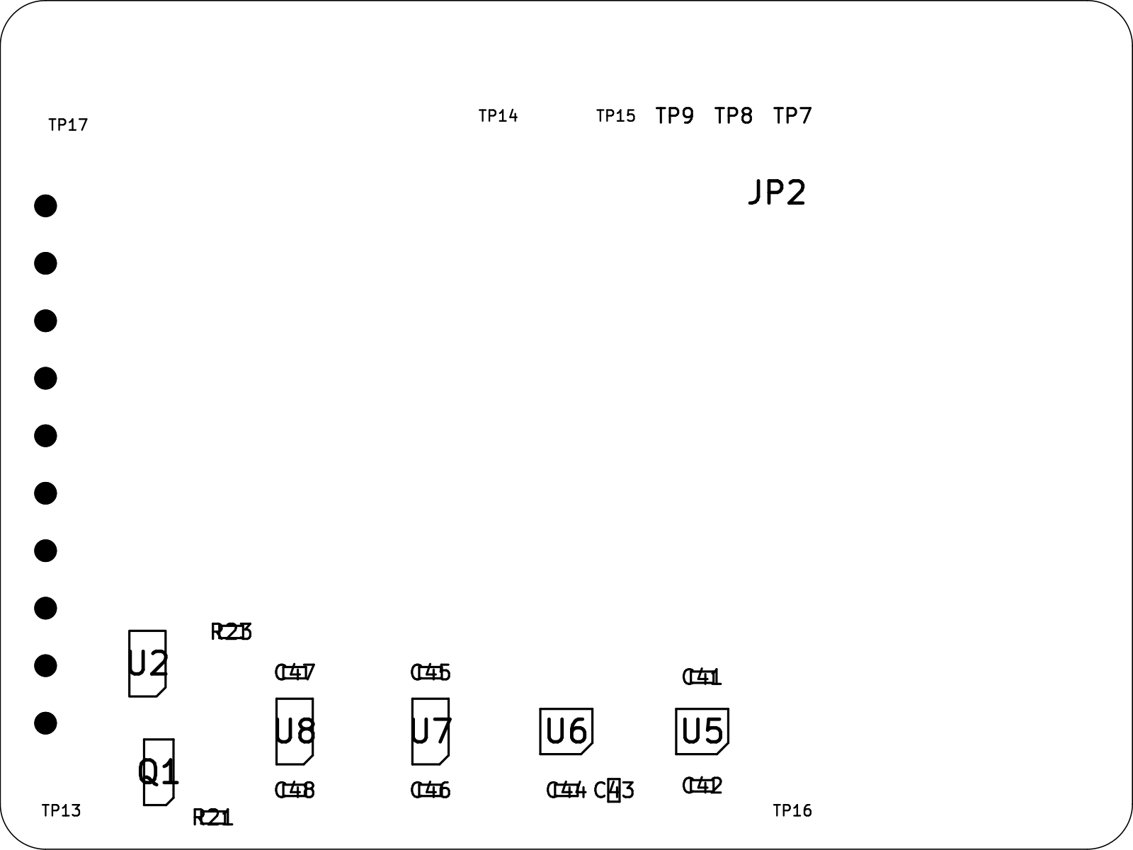
NRF9161-v2-panel is an open-source printed circuit board by anand2532, from the anand2532/nRF9161-DEV-BOARD repository on GitHub. It is a 4-layer board of 118 × 93 mm with 474 parts on 480 nets, routed with 3,300 tracks and 992 vias.
It is built around the NRF9161-LACA-R7, SN74LXC1T45DBV and SN74LXC2T45DCU, with the TLV73333PDBV, TPD3F303DPVR and BLM18KG221SN1 among its other parts. Its parts include 160 capacitors, 32 ICs, 24 resistors, 20 connectors and 16 diodes.


A small 50 × 37.5 mm LTE-M / NB-IoT + GNSS modem board built around the Nordic nRF9161. Any host MCU controls it with AT commands over one 10-pin UART header.
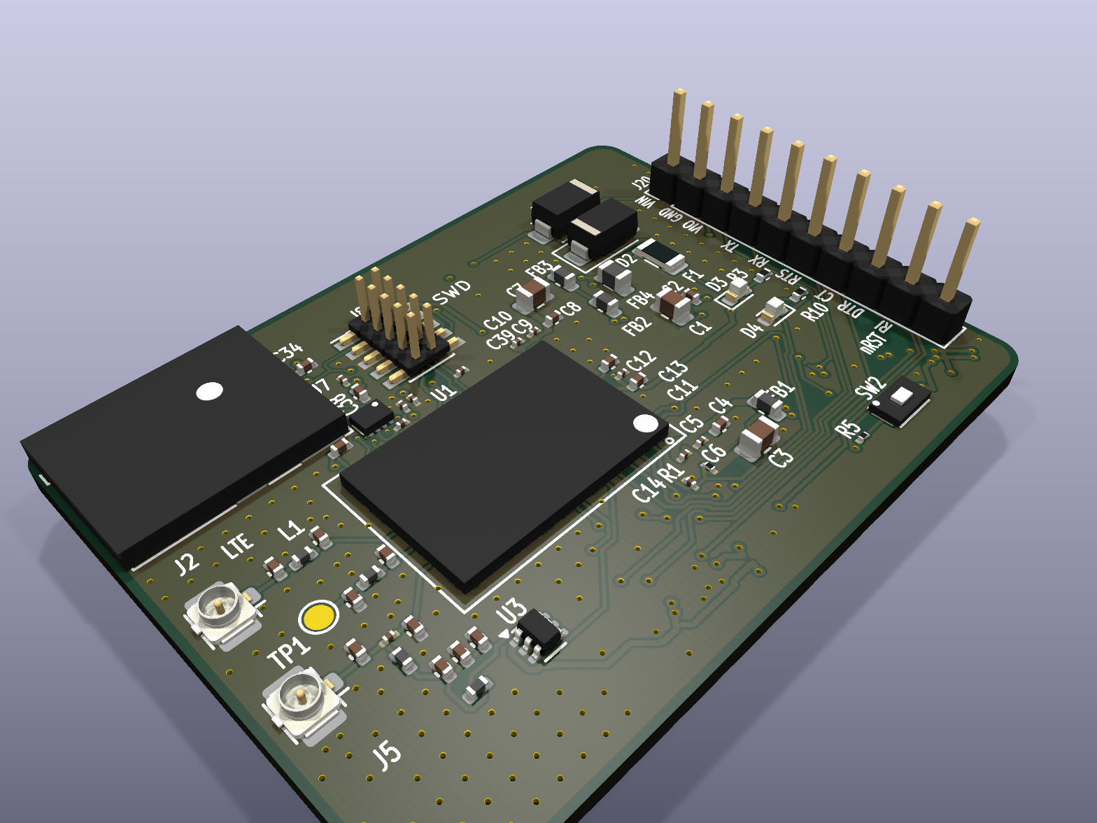
Status: v2 has passed DRC (0 errors, 0 unconnected), ERC (0 errors), schematic parity, an RF review and a DFM review. The JLCPCB fab and assembly package is in
fab/staging-v2-36d8578/. It has not been ordered yet.
flowchart LR
  HOST["Host MCU<br/>(1.8 / 3.3 / 5 V)"] -- "J20: TX RX RTS CTS DTR RI" --> LS["SN74LXC2T45 ×2<br/>SN74LXC1T45 ×2<br/>(VIO ↔ 3.3 V)"]
  HOST -- "J20: nRESET" --> Q1["Q1 BSS138<br/>open-drain"]
  LS --> U1["nRF9161-LACA-R7<br/>LTE-M / NB-IoT / GNSS"]
  Q1 --> U1
  VIN["J20 VIN 3.0–5.5 V"] --> PROT["D1 SS34 · D2 SMAJ5.0A<br/>F1 2 A · FB4"] --> U1
  PROT --> LDO["U2 TLV73333<br/>3.3 V VDD_GPIO"] --> LS
  U1 -- "SIM_RST/CLK/IO/1V8" --> ESD["U4 TPD3F303"] --> SIM["J7 nano-SIM"]
  U1 -- "ANT" --> J2["J2 U.FL LTE"]
  U1 -- "GPS" --> J5["J5 U.FL GNSS"]
  LDO --> SW["U3 TPS22919<br/>(COEX0)"] -- "active-antenna bias" --> J5
  SWD["J8 SWD 2×5 1.27 mm"] --- U1
U1 -- "P0.00" --> D4["D4 status / network LED"]| Pin | Name | Direction (host view) | Modem side |
|---|---|---|---|
| 1 | VIN | power in | 3.0–5.5 V supply |
| 2 | GND | — | ground |
| 3 | VIO | reference in | host logic rail, 1.1–5.5 V (feeds the translators; not an output) |
| 4 | TX | host → modem | P0.03, UART RXD (via U5) |
| 5 | RX | modem → host | P0.02, UART TXD (via U6) |
| 6 | RTS | host → modem | P0.07, modem CTS (via U5) |
| 7 | CTS | modem → host | P0.06, modem RTS (via U6) |
| 8 | DTR | host → modem, active-low | P0.31 (via U7, 100k pull-up to VIO) |
| 9 | RI | modem → host, active-low | P0.30 (via U8) |
| 10 | nRESET | host → modem, active-low | open-drain through Q1 BSS138 (5 V safe) |
The RTS/CTS crossover is done on the board, so wire J20 straight across to the host pins with the same names. Full details: docs/PINOUT.md.
Host MCU            J20
3V3 / 5V  ───────── 1 VIN   (must supply ~500 mA LTE TX peaks)
GND       ───────── 2 GND
3V3 (IO)  ───────── 3 VIO
UART TX   ───────── 4 TX
UART RX   ───────── 5 RX
UART RTS  ───────── 6 RTS
UART CTS  ───────── 7 CTS
GPIO (out)───────── 8 DTR   (optional; pull low to wake)
GPIO (in) ───────── 9 RI    (optional)
GPIO (OD) ───────── 10 nRESET (optional)
UART settings: 115200 baud, 8N1, hardware flow control (as in the Serial Modem external-mcu.overlay).
| Parameter | Value |
|---|---|
| Modem | nRF9161-LACA-R7 (LTE-M, NB-IoT, GNSS) |
| Supply (VIN) | 3.0–5.5 V. Input TVS is 5.0 V; 2 A fuse |
| Host logic (VIO) | 1.1–5.5 V (SN74LXC range) |
| Internal GPIO rail | 3.3 V (TLV73333) |
| Peak current | about 500 mA on LTE TX (VDD2). Use a 1 A-limited supply for bring-up |
| Host UART | 115200 baud, RTS/CTS, DTR, RI |
| Antennas | U.FL LTE (J2); U.FL GNSS, active antenna (J5) |
| SIM | nano-SIM 4FF (JAE SF72S006) |
| Debug | SWD, 2×5 1.27 mm (J8) |
| Board size | 50.05 × 37.55 mm, R2.0 corners |
| PCB | 4 layers, 1.6 mm FR4, ENIG, 1 oz; stackup 0.12 / 1.2 / 0.12 mm |
| Vias | 30 epoxy-filled and capped (POFV) per board: 21 × 0.20 mm, 9 × 0.25 mm |
| Assembly | double-sided: 51 top, 16 bottom (67 parts) |
| Ref | Part | Function | LCSC |
|---|---|---|---|
| U1 | NRF9161-LACA-R7 | LTE-M / NB-IoT / GNSS SiP | C21547412 |
| U2 | TLV73333PDBV | 3.3 V LDO (VDD_GPIO) | C134139 |
| U3 | TPS22919DCKR | GNSS active-antenna bias switch | C2149796 |
| U4 | TPD3F303DPV | SIM ESD protection | C2865991 |
| U5, U6 | SN74LXC2T45 | UART level shifters | C5217891 |
| U7, U8 | SN74LXC1T45 | DTR / RI level shifters | C4364198 |
| Q1 | BSS138 | open-drain reset isolator | C52895 |
| D1 | SS34 | reverse-polarity Schottky | C8678 |
| D2 | SMAJ5.0A | VIN TVS | C10758 |
| F1 | 2 A 1206 fuse | input fuse | C187611 |
| J2, J5 | Hirose U.FL-R-SMT-1(10) | LTE / GNSS antenna | C88373 |
| J7 | JAE SF72S006 | nano-SIM holder | C2977286 |
| J8 | 2×5 1.27 mm SMD header | SWD | C5155080 |
| J20 | 1×10 2.54 mm header | host interface | C57369 |
| SW2 | C&K KXT3 | reset button | C778127 |
| D3, D4 | LTST-C191KGKT green 0603 | power / status LEDs | C125098 |
Full BOM and placement: jlc/BOM_JLC_v2.csv, jlc/CPL_JLC_v2.csv, master jlc/BOM.csv.
| Top | Bottom |
|---|---|
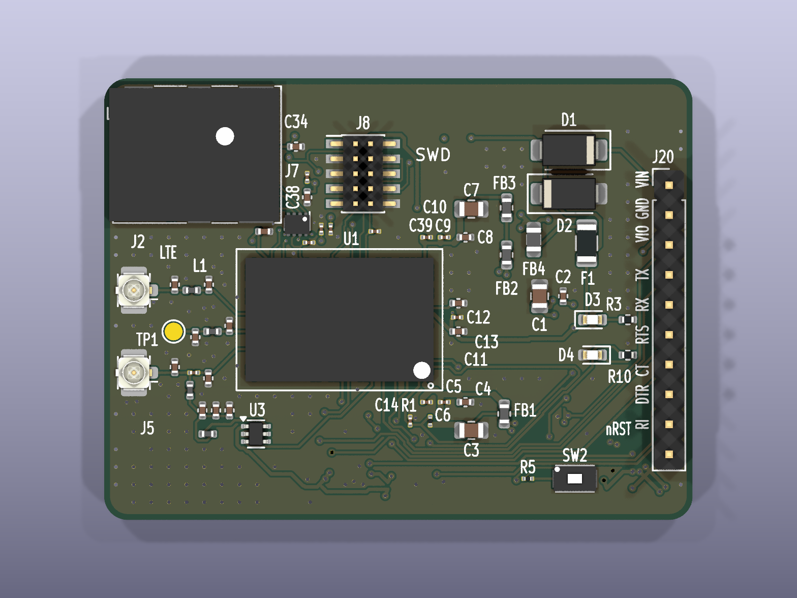 | 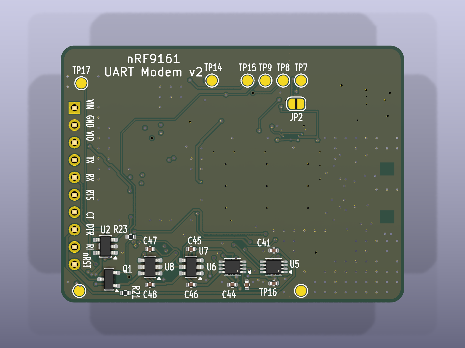 |
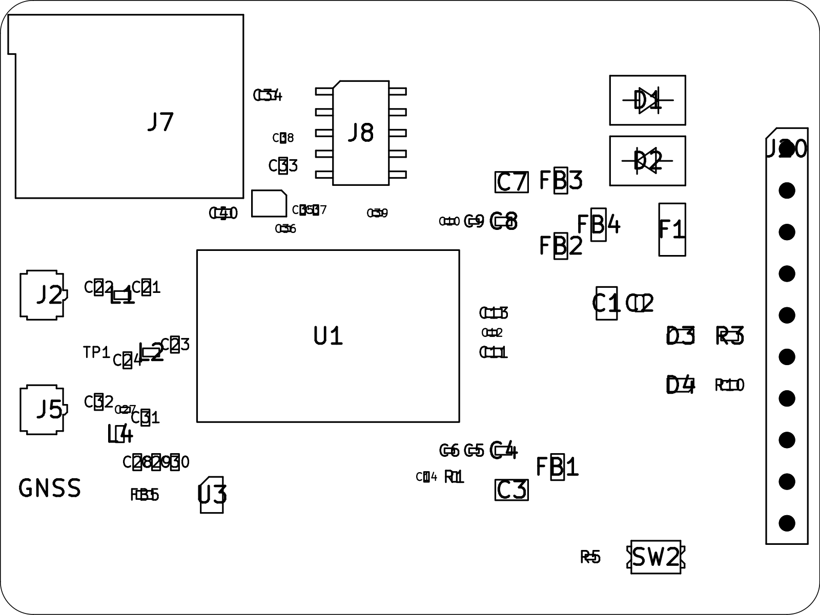 |  |
nrf9161dk/nrf9161/ns with the external-MCU overlay, which matches this board's pins with no changes:
west build -b nrf9161dk/nrf9161/ns app -- -DEXTRA_DTC_OVERLAY_FILE=external-mcu.overlay
west flash   # J-Link on J8
# or: nrfjprog -f NRF91 --program merged.hex --chiperase --verify --resetAT -> OK
AT+CGMR -> modem firmware version
AT+CFUN=1 -> radio on
AT+CEREG=5 -> enable registration notifications
AT+CEREG? -> +CEREG: 5,1,... (1 = home, 5 = roaming)
AT%XMONITOR -> network/cell info
AT+CFUN=0 -> radio offD4 sits on P0.00 (through R10, 1 kΩ, active-high). The Serial Modem app has no built-in network LED, so add about 20 lines of app code: subscribe to LTE registration events and drive P0.00 high on registered home/roaming, low otherwise. No hardware change is needed. In the board overlay, define a gpio-leds node on &gpio0 0 GPIO_ACTIVE_HIGH and disable the unused nRF9161 DK led0–3 and button nodes.
AT%XCOEX0).Order the panel: fab/staging-v2-36d8578/nRF9161-v2-panel-36d8578.zip, a 2×2 panel of 118.10 × 93.10 mm with mouse-bite tabs, a 6 mm frame and fiducials. The full instructions are in fab/staging-v2-36d8578/ORDER_NOTES.md and docs/FAB_READY_CHECKLIST_V2.md.
JLC assembly uses the LCSC parts in jlc/. Indian sourcing is for hand assembly, rework or spares. See india/README.md for Indian PCB fab and assembly vendors (with which ones can likely make the 0.20 mm filled vias) and for component vendors. The per-part sourcing list is india/BOM_INDIA.csv (Robu, then LionCircuits, with URLs, INR prices and stock).
.
├── README.md
├── hardware/                 KiCad 9 project (open hardware/nRF9161-DEV-BOARD.kicad_pro)
│   ├── nRF9161-DEV-BOARD.kicad_{pro,pcb,sch,dru,prl}
│   ├── schematic/            hierarchical sheets 01–12
│   ├── libraries/            project symbols + footprints (Board.pretty, Nordic_*)
│   ├── 3dmodels/             placeholder STEP models
│   ├── panel/                2×2 JLC panel project
│   └── fp-lib-table, sym-lib-table   (${KIPRJMOD}-relative)
├── jlc/                      BOM_JLC_v2.csv, CPL_JLC_v2.csv, master BOM.csv
├── india/                    India sourcing: BOM_INDIA.csv/.xlsx, fab + parts vendor guide
├── fab/
│   ├── staging-v2-36d8578/   current fab package (single + panel zips, ORDER_NOTES)
│   └── archive/              older staging packages and v1 outputs
├── docs/                     pinout, fab checklist, stackup, reviews
│   └── reports/              design, RF, DFM and DRC/ERC reports
├── images/                   renders and assembly drawings
└── tools/ helper scripts| Version | Branch | Notes |
|---|---|---|
| v1 | v1-dev-board | Full breakout development board (120 × 80 mm, many headers) |
| v2 | main | UART modem module: breakouts removed, single J20 host header with level shifters, 50.05 × 37.55 mm, double-sided assembly, U4 DPV footprint fixed, JLC-ready |
This hardware design is licensed under the CERN Open Hardware Licence Version 2 – Permissive (CERN-OHL-P v2). See LICENSE for the full text.
Copyright 2026 Anand Mohan Pandey. SPDX-License-Identifier: CERN-OHL-P-2.0
| Qty | Value | Footprint | References |
|---|---|---|---|
| 132 | NPTH | NPTH | KiKit_MB_10_1, KiKit_MB_10_2, KiKit_MB_10_3, KiKit_MB_10_4, KiKit_MB_10_5, KiKit_MB_11_1, KiKit_MB_11_2, KiKit_MB_11_3, KiKit_MB_11_4, KiKit_MB_11_5, KiKit_MB_12_1, KiKit_MB_12_2, KiKit_MB_12_3, KiKit_MB_12_4, KiKit_MB_12_5, KiKit_MB_13_1 +116 |
| 48 | 100nF | Capacitor_SMD:C_0402_1005Metric | C2, C2, C2, C2, C30, C30, C30, C30, C33, C33, C33, C33, C40, C40, C40, C40 +32 |
| 24 | DNP | Capacitor_SMD:C_0402_1005Metric | C21, C21, C21, C21, C22, C22, C22, C22, C23, C23, C23, C23, C24, C24, C24, C24 +8 |
| 16 | 100nF | Capacitor_SMD:C_0201_0603Metric | C5, C5, C5, C5, C9, C9, C9, C9, C12, C12, C12, C12, C14, C14, C14, C14 |
| 16 | 22pF | Capacitor_SMD:C_0201_0603Metric | C35, C35, C35, C35, C36, C36, C36, C36, C37, C37, C37, C37, C38, C38, C38, C38 |
| 16 | 4.7uF | Capacitor_SMD:C_0402_1005Metric | C4, C4, C4, C4, C8, C8, C8, C8, C11, C11, C11, C11, C13, C13, C13, C13 |
| 12 | BLM18KG221SN1 | Inductor_SMD:L_0603_1608Metric | FB1, FB1, FB1, FB1, FB2, FB2, FB2, FB2, FB3, FB3, FB3, FB3 |
| 8 | 0R | Inductor_SMD:L_0402_1005Metric | L1, L1, L1, L1, L2, L2, L2, L2 |
| 8 | 100k | Resistor_SMD:R_0402_1005Metric | R21, R21, R21, R21, R23, R23, R23, R23 |
| 8 | 15pF | Capacitor_SMD:C_0201_0603Metric | C6, C6, C6, C6, C10, C10, C10, C10 |
| 8 | 1k | Resistor_SMD:R_0402_1005Metric | R3, R3, R3, R3, R10, R10, R10, R10 |
| 8 | 47uF/10V | Capacitor_SMD:C_0805_2012Metric | C3, C3, C3, C3, C7, C7, C7, C7 |
| 8 | Green LED | LED_SMD:LED_0603_1608Metric | D3, D3, D3, D3, D4, D4, D4, D4 |
| 8 | SN74LXC1T45 | Package_TO_SOT_SMD:SOT-23-6 | U7, U7, U7, U7, U8, U8, U8, U8 |
| 8 | SN74LXC2T45 | Package_SO:VSSOP-8_2.3x2mm_P0.5mm | U5, U5, U5, U5, U6, U6, U6, U6 |
| 6 | Fiducial | Fiducial | KiKit_FID_B_1, KiKit_FID_B_2, KiKit_FID_B_3, KiKit_FID_T_1, KiKit_FID_T_2, KiKit_FID_T_3 |
| 4 | 100nH | Inductor_SMD:L_0402_1005Metric | L4, L4, L4, L4 |
| 4 | 100pF | Capacitor_SMD:C_0201_0603Metric | C27, C27, C27, C27 |
| 4 | 100pF | Capacitor_SMD:C_0402_1005Metric | C28, C28, C28, C28 |
| 4 | 10k | Resistor_SMD:R_0201_0603Metric | R1, R1, R1, R1 |
| 4 | 10nF | Capacitor_SMD:C_0402_1005Metric | C29, C29, C29, C29 |
| 4 | 10uF/16V | Capacitor_SMD:C_0805_2012Metric | C1, C1, C1, C1 |
| 4 | 1k | Resistor_SMD:R_0201_0603Metric | R5, R5, R5, R5 |
| 4 | 220nF | Capacitor_SMD:C_0402_1005Metric | C34, C34, C34, C34 |
| 4 | 2A | Fuse:Fuse_1206_3216Metric | F1, F1, F1, F1 |
| 4 | AUX | TestPoint:TestPoint_Pad_D1.5mm | TP1, TP1, TP1, TP1 |
| 4 | BLM15HG102SN1 | Inductor_SMD:L_0402_1005Metric | FB5, FB5, FB5, FB5 |
| 4 | BLM21PG221SN1 | Inductor_SMD:L_0805_2012Metric | FB4, FB4, FB4, FB4 |
| 4 | BSS138 | Package_TO_SOT_SMD:SOT-23 | Q1, Q1, Q1, Q1 |
| 4 | DNP | Capacitor_SMD:C_0201_0603Metric | C39, C39, C39, C39 |
| 4 | ENABLE | TestPoint:TestPoint_Pad_D1.5mm | TP17, TP17, TP17, TP17 |
| 4 | GND | TestPoint:TestPoint_Pad_D1.5mm | TP16, TP16, TP16, TP16 |
| 4 | HOST_1x10_2.54 | Connector_PinHeader_2.54mm:PinHeader_1x10_P2.54mm_Vertical | J20, J20, J20, J20 |
| 4 | NRF9161-LACA-R7 | Board:nRF9161_LGA_16.0x10.5mm | U1, U1, U1, U1 |
| 4 | RESET | Button_Switch_SMD:SW_SPST_CK_KXT3 | SW2, SW2, SW2, SW2 |
| 4 | SIM_VCC | Jumper:SolderJumper-2_P1.3mm_Open_RoundedPad1.0x1.5mm | JP2, JP2, JP2, JP2 |
| 4 | SMAJ5.0A | Diode_SMD:D_SMA | D2, D2, D2, D2 |
| 4 | SS34 | Diode_SMD:D_SMA | D1, D1, D1, D1 |
| 4 | SWCLK | TestPoint:TestPoint_Pad_D1.5mm | TP8, TP8, TP8, TP8 |
| 4 | SWDIO | TestPoint:TestPoint_Pad_D1.5mm | TP7, TP7, TP7, TP7 |
| 4 | SWD_10pin | Connector_PinHeader_1.27mm:PinHeader_2x05_P1.27mm_Vertical_SMD | J8, J8, J8, J8 |
| 4 | TLV73333PDBV | Package_TO_SOT_SMD:SOT-23-5 | U2, U2, U2, U2 |
| 4 | TPD3F303DPV | Board:TI_TPD3F303_USON-8_DPV_2.1x1.6mm_P0.5mm | U4, U4, U4, U4 |
| 4 | TPS22919DCKR | Package_TO_SOT_SMD:SOT-363_SC-70-6 | U3, U3, U3, U3 |
| 4 | U.FL_GNSS | Connector_Coaxial:U.FL_Hirose_U.FL-R-SMT-1_Vertical | J5, J5, J5, J5 |
| 4 | U.FL_LTE_NR+ | Connector_Coaxial:U.FL_Hirose_U.FL-R-SMT-1_Vertical | J2, J2, J2, J2 |
| 4 | VDD_GPIO | TestPoint:TestPoint_Pad_D1.5mm | TP13, TP13, TP13, TP13 |
| 4 | VDD_nRF | TestPoint:TestPoint_Pad_D1.5mm | TP14, TP14, TP14, TP14 |
| 4 | VIN | TestPoint:TestPoint_Pad_D1.5mm | TP15, TP15, TP15, TP15 |
| 4 | nRESET | TestPoint:TestPoint_Pad_D1.5mm | TP9, TP9, TP9, TP9 |
| 4 | nanoSIM_4FF | Connector_JAE:JAE_SIM_Card_SF72S006 | J7, J7, J7, J7 |
anand2532/nRF9161-DEV-BOARD
A small 50 × 37.5 mm LTE-M / NB-IoT + GNSS modem board built around the Nordic nRF9161. Any host MCU controls it with AT commands over one 10-pin UART header.


PimentoFr/plant-monitor
Developpement d'un capteur de potager indoor/outdoorn solaire et connecté via Sigfox


GManSudy/framework-expansion-lte
An LTE-M / NB-IoT cellular modem built into the Framework Laptop Expansion Card form factor, with a native USB-C plug.


mickaelly01nobre/-Printed-Circuit-Board-PCB-
Este projeto envolve o desenvolvimento de uma Placa de Circuito Impresso (PCB) baseada na placa de demonstração STEVAL-ISV012V1.
It measures 118 × 93 mm and has 4 copper layers, 1.6 mm thick.
474 parts, built around the NRF9161-LACA-R7, SN74LXC1T45DBV, SN74LXC2T45DCU and TLV73333PDBV. The full list of its parts is on this page, with links to each part's symbol and footprint where PCBKit's library has them.
From the anand2532/nRF9161-DEV-BOARD repository on GitHub, at the commit this page was made from: the board is hardware/panel/nRF9161-v2-panel.kicad_pcb and its schematic hardware/nRF9161-DEV-BOARD.kicad_sch. PCBKit opens the board in the browser, with nothing to install.
Its repository states no licence, so its author keeps all rights: ask anand2532 before reusing the design.