2 layers27.9 × 16.5 mm

 alexandarZ/QRPChokeTestJig
A small PCB test jig for measuring common-mode attenuation, insertion loss and VSWR of QRP common-mode chokes (CMC)
QRP CMC Choke Test Jig is an open-source printed circuit board by alexandarZ, from the alexandarZ/QRPChokeTestJig repository on GitHub, published under the CC-BY-SA-4.0 licence. It is a 2-layer board of 55.3 × 53.2 mm with 18 parts on 11 nets, routed with 27 tracks and 160 vias.
Its parts include 11 switches and 2 resistors. It belongs with the radio and wireless boards of this library.
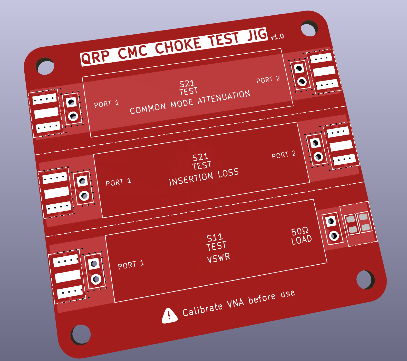
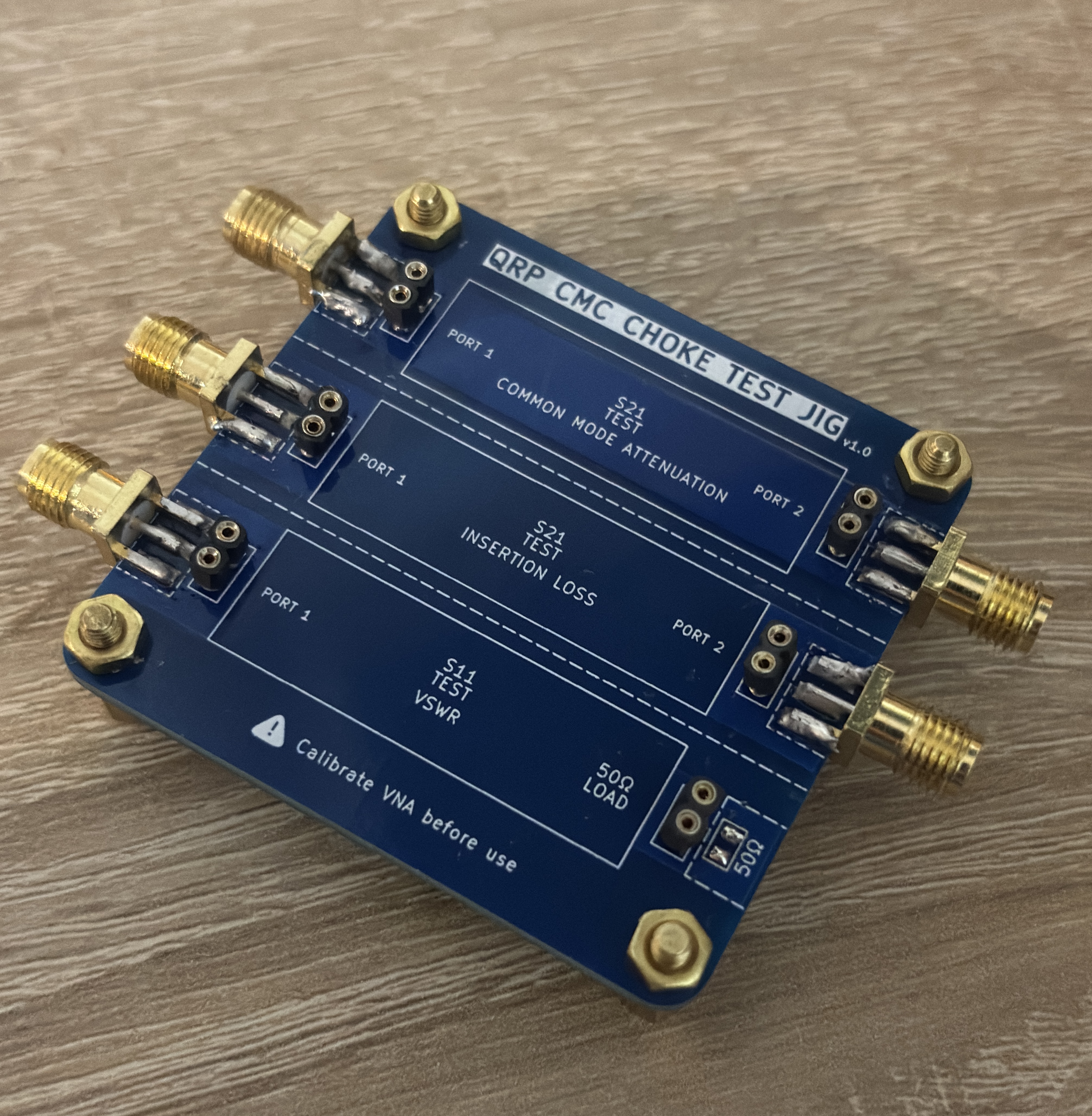
The QRP CMC Choke Test Jig is a compact PCB test fixture that makes evaluating small common-mode chokes like FT140 and below fast, repeatable and convenient. Designed for use with a handheld VNA (e.g. NanoVNA), the board provides dedicated SMA test ports and simple wiring options to measure the choke’s common-mode attenuation (S21), insertion loss (S21) and reflection / matching (S11 / VSWR) under consistent conditions.
A built-in ~50 Ω termination (two 100 Ω SMD resistors in parallel) and configurable female headers remove the need for ad-hoc fixtures or awkward cable rigs, so you can quickly compare different choke constructions, spot resonances, and quantify how the choke affects the desired signal path. Intended for QRP choke testing, the jig speeds prototyping, helps validate designs for real-world use, and standardizes measurements so results are easier to reproduce and share.
Gerber package (manufacturing files):
/gerbers/QRP_CMC_Choke_Test_Jig_v1_0.zip
| Qty | Part | Value / Type | Notes |
|---|---|---|---|
| 5 | SMA connector, PCB mount (female) | SMA-F, PCB-mount | 5 positions for test ports |
| 6 | Female header (single-row) | 2.54 mm female socket | For test jumpers / optional wiring |
| 2 | SMD resistor | 100 Ω 0805 | Two in parallel → ~50 Ω termination |
| 1 | PCB | QRP CMC Choke Test Jig v1.0 | Use Gerbers in /gerber |
Termination note: Two 100 Ω resistors in parallel produce approximately 50 Ω (R_eq = 1 / (1/100 + 1/100) = 50 Ω). This is a practical, low-power test termination for S11/SWR checks at QRP power levels. Verify resistor power rating if higher transmit power is expected.
Contributions welcome:
| Qty | Value | Footprint | References |
|---|---|---|---|
| 6 | Conn_01x02_Pin | Connector_PinSocket_2.54mm:PinSocket_1x02_P2.54mm_Vertical | S11_J1, S11_J2, S21_J1, S21_J2, S21_J3, S21_J4 |
| 5 | SMA_Edge | PCM_SparkFun-Connector:SMA_Edge_8mm | S11, S21_A1, S21_B1, S21_C1, S21_D1 |
| 2 | 100R | PCM_Resistor_SMD_AKL:R_0805_2012Metric | R1, R2 |
The 13 most common of 18 parts.

VoronDesign/Voron-Hardware
Cool Hardware designed by the Voron Design group


hackclub/OnBoard
💡 Join 1,000 teenagers and make your first PCB with a $100 grant!

VoronDesign/Voron-Tap
Tap is a nozzle-based z-probe for the V2 and Trident printer designs. The entire toolhead moves to trigger an optical switch. Tap offers many advantages:

Luos-io/luos_engine
Open-source and real-time orchestrator for cyber-physical-systems, to easily design, test and deploy embedded applications and digital twins.


Twotoz/C5VRX
Ultra-minimal, zero-CPU 5.8 GHz analog FPV video receiver using ESP32-C5 Wi-Fi 6 PHY MODEM_DIAG, BitScrambler WBFM demodulation & resistor DAC CVBS
It measures 55.3 × 53.2 mm and has 2 copper layers, 1.6 mm thick.
18 parts. The full list of its parts is on this page, with links to each part's symbol and footprint where PCBKit's library has them.
From the alexandarZ/QRPChokeTestJig repository on GitHub, at the commit this page was made from: the board is project/QRP_CMC_Choke_Test_Jig.kicad_pcb and its schematic project/QRP_CMC_Choke_Test_Jig.kicad_sch. PCBKit opens the board in the browser, with nothing to install.
Its repository publishes it under the CC-BY-SA-4.0 licence: you may reuse it on that licence's terms (keep the author's notice, and for a copyleft licence share your changes alike).