2 layers31.5 × 24.5 mm
Proejtc
abhictrl/IEEE-HOPE-FSO
A laser-based audio communication link for the Howard University IEEE H.O.P.E. Project.
4 partsMIT

 abhictrl/IEEE-HOPE-FSO
A laser-based audio communication link for the Howard University IEEE H.O.P.E. Project.
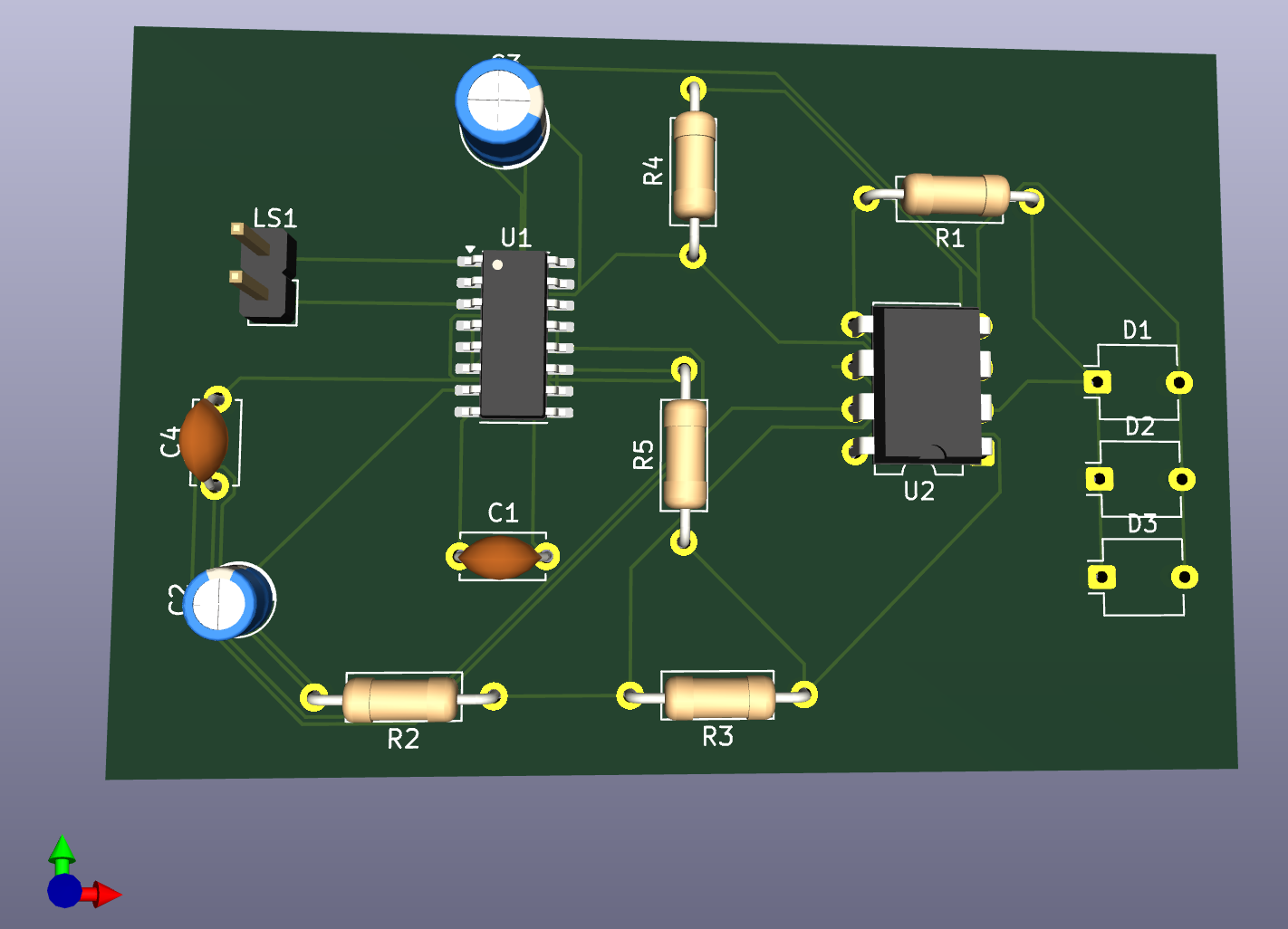
Receiver board is an open-source printed circuit board by abhictrl, from the abhictrl/IEEE-HOPE-FSO repository on GitHub, published under the MIT licence. It is a 2-layer board of 65.5 × 43.5 mm with 15 parts on 14 nets, routed with 124 tracks and 0 vias.
It is built around the LM358, PAM8403DR and BPW34. Its parts include 5 resistors, 4 capacitors, 3 diodes and 2 ICs. It belongs with the audio and music boards of this library.


A laser-based audio communication system built for the Howard University IEEE H.O.P.E. (Hands-On PCB Engineering) Project (Fall 2025).
Project Lux is a free-space optical (FSO) communication system that transmits a high-fidelity audio signal over a laser beam.
This project demonstrates the core principles of optical communication. The system consists of two main components:
This creates a simple, point-to-point wireless audio link.
BPW34) detects the modulated laser beam and converts it back into an electrical signal.The transmitter board is the "voice" of the system. Its job is to take a standard audio signal and convert it into a light-based signal by modulating the brightness of a laser.
R1, R2) creates a 2.5V "virtual ground." An AC-coupling capacitor (C1) lets the audio signal "ride" on top of this 2.5V bias, shifting the entire wave into the positive (1.5V to 3.5V) range.U1A) buffers the signal, which then drives a transistor (Q1). The transistor acts as a "valve," controlling the current flowing through the laser.R6_Variable) is used to set the "quiescent" or "idle" current. This keeps the laser on at "half-brightness" when no audio is playing, allowing the signal to modulate both brighter and dimmer.Q1 drives the laser diode (LD1), causing its brightness to flicker in perfect sync with the audio waveform.The receiver board is the "ear" of the system, designed to convert the incoming light signal back into audible sound. The signal path is a three-stage process.
BPW34 photodiodes captures the modulated laser light, generating a tiny electrical current proportional to the light's brightness.U2A) is configured as a Transimpedance Amplifier (TIA). It converts this weak input current into a usable voltage signal.U2B), which is configured as an inverting gain stage to boost the signal.1uF capacitor (C2) blocks the DC component of the signal, passing only the clean AC audio to the final stage.PAM8403D Class-D audio amplifier takes the line-level signal and provides the necessary power to drive a standard 4S1 speaker.BPW34 (x3)LM358PAM8403DWant more detail?
Check out the Full Circuit Walkthrough for a component-by-component explanation of the schematics.
This repository is organized to keep our hardware designs, firmware code, and documentation separate and clean.
/
├── hardware/
│   ├── Receiver board/     # KiCad project files for the receiver
│   └── Transmitter board/  # KiCad project files for the transmitter
├── firmware/
│   └── ...                 # Arduino C++ source code (coming soon)
├── media/
│   └── pictures
|         └─...                 # Schematics, 3D renders, and demo videos
├── docs/
│   └── Walkthrough.md               # Datasheets, presentations, etc.
├── .gitignore
└── README.mdThis project is currently in progress.
This project is heavily inspired by the "Laser Audio Transmitter" final project from Cornell University's ECE 4760 course.
This project is licensed under the MIT License. See the LICENSE file for full details.
| Qty | Value | Footprint | References |
|---|---|---|---|
| 4 | 10k | Resistor_THT:R_Axial_DIN0207_L6.3mm_D2.5mm_P10.16mm_Horizontal | R1, R2, R4, R5 |
| 3 | BPW34 | OptoDevice:Osram_DIL2_4.3x4.65mm_P5.08mm | D1, D2, D3 |
| 2 | 0.1uF | Capacitor_THT:C_Disc_D4.7mm_W2.5mm_P5.00mm | C1, C4 |
| 1 | 1uF | Capacitor_THT:CP_Radial_D4.0mm_P1.50mm | C2 |
| 1 | 20uF | Capacitor_THT:CP_Radial_D5.0mm_P2.50mm | C3 |
| 1 | 5.1k | Resistor_THT:R_Axial_DIN0207_L6.3mm_D2.5mm_P10.16mm_Horizontal | R3 |
| 1 | LM358 | Package_DIP:DIP-8_W7.62mm | U2 |
| 1 | PAM8403D | Package_SO:SOIC-16_3.9x9.9mm_P1.27mm | U1 |
| 1 | Speaker | Connector_PinHeader_2.54mm:PinHeader_1x02_P2.54mm_Vertical | LS1 |
abhictrl/IEEE-HOPE-FSO
A laser-based audio communication link for the Howard University IEEE H.O.P.E. Project.

RobertGawron/SemiconductorRadioactivityDetector
Nuclear radiation sensor with photodiode as a detector. Photodiode doesn't require high voltages as GM tubes do. Smaller size makes better resolution. Side effect is electronic must be more sensitive.


QuantumVillage/UncutGem
A prototype Full Stack fully Open Source NV Center Diamond Magnetometer

Roboy/HTC_Vive_Sensors
Schematics and PCB designs for our custom Vive sensors based on a quad op-amp chip rather than discrete transistors.
It measures 65.5 × 43.5 mm and has 2 copper layers, 1.6 mm thick.
15 parts, built around the LM358, PAM8403DR and BPW34. The full list of its parts is on this page, with links to each part's symbol and footprint where PCBKit's library has them.
From the abhictrl/IEEE-HOPE-FSO repository on GitHub, at the commit this page was made from: the board is hardware/Receiver board/Circuit.kicad_pcb and its schematic hardware/Receiver board/Circuit.kicad_sch. PCBKit opens the board in the browser, with nothing to install.
Its repository publishes it under the MIT licence: you may reuse it on that licence's terms (keep the author's notice, and for a copyleft licence share your changes alike).