
2 layers68.6 × 53.3 mm
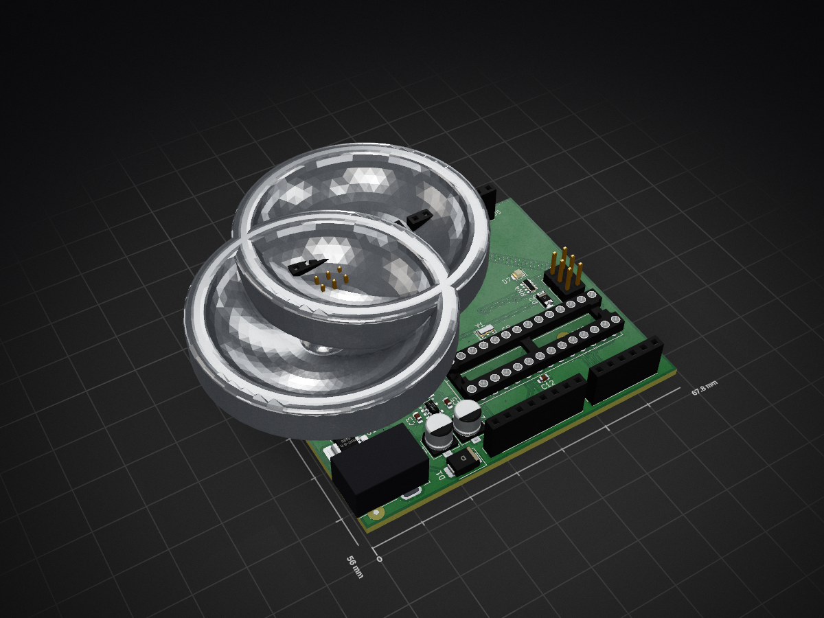
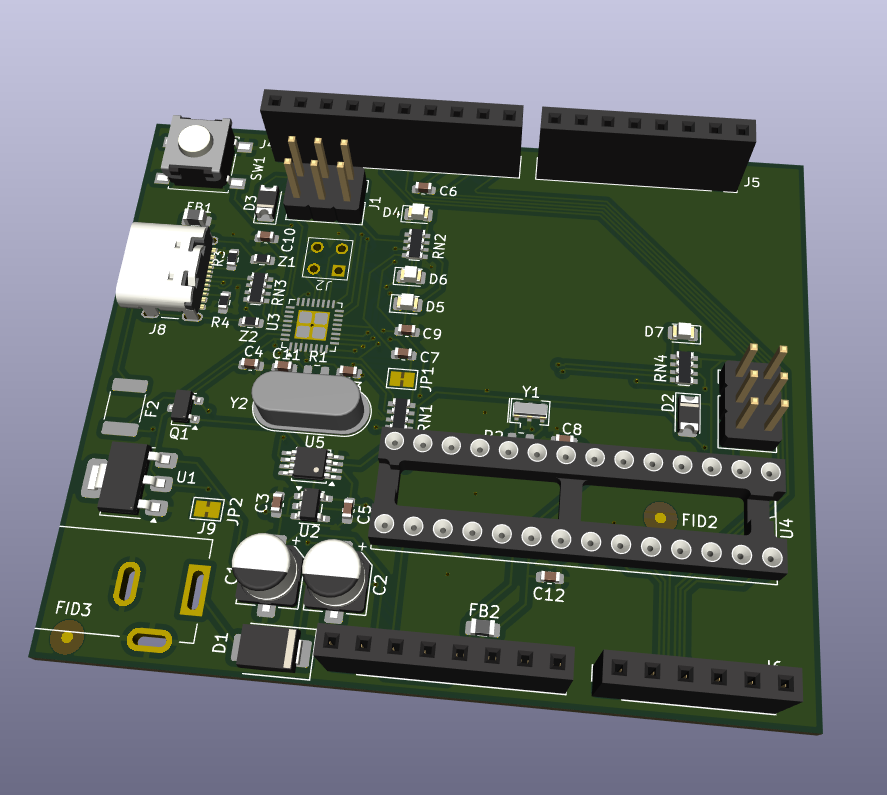
Custom Arduino Uno-compatible PCB designed in KiCad, including schematic, PCB layout, routing, and 3D visualization.
Arduino is an open-source printed circuit board by aarthirethinabala, from the aarthirethinabala/Arduino-Uno-Compatible-PCB repository on GitHub. It is a 2-layer board of 67.8 × 56 mm with 56 parts on 79 nets, routed with 724 tracks and 60 vias.
It is built around the ATMEGA16U2-MU, ATMEGA328P-PU and LMV358IDGKR, with the LP2985-33DBV and FDN340P among its other parts. Its parts include 13 capacitors, 9 connectors, 7 diodes, 5 ICs and 4 resistors. It belongs with the AVR (ATmega, ATtiny) boards of this library.


Custom Arduino Uno-compatible PCB designed in KiCad, including schematic design, component footprint assignment, PCB layout, routing, and 3D visualization.
Completed
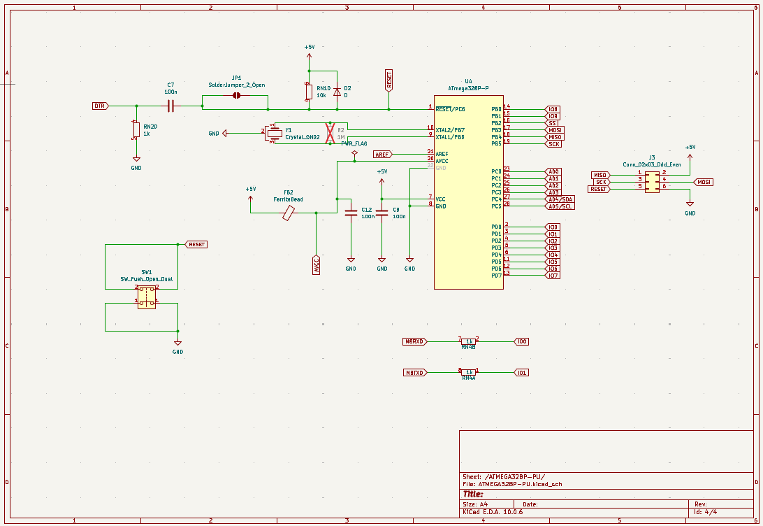
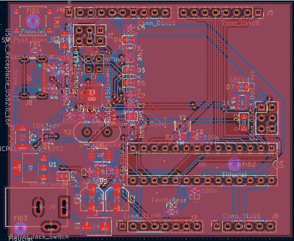
This project involved designing an Arduino Uno-compatible printed circuit board(PCB) from the schematic stage through PCB layout and design-rule checking. The design was created in KiCad and includes the major components and connections required for an Arduino Uno-compatible board.
The PCB was developed through the following stages:
The schematic and PCB layout have been completed and checked using KiCad's ERC and DRC tools. The final design includes routed connections, vias, copper zones, and the complete board outline.
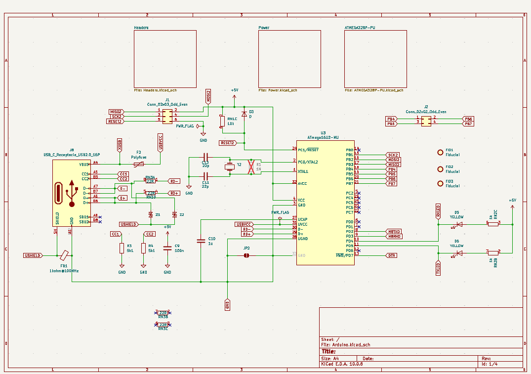
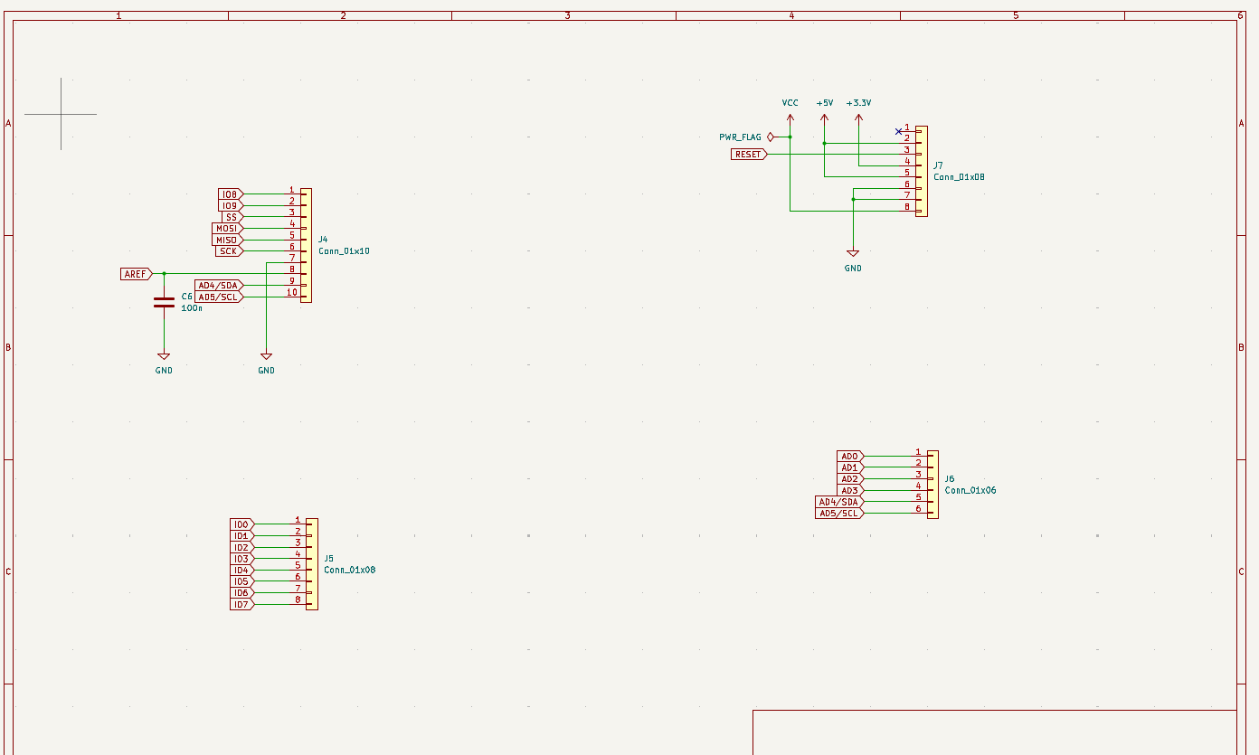
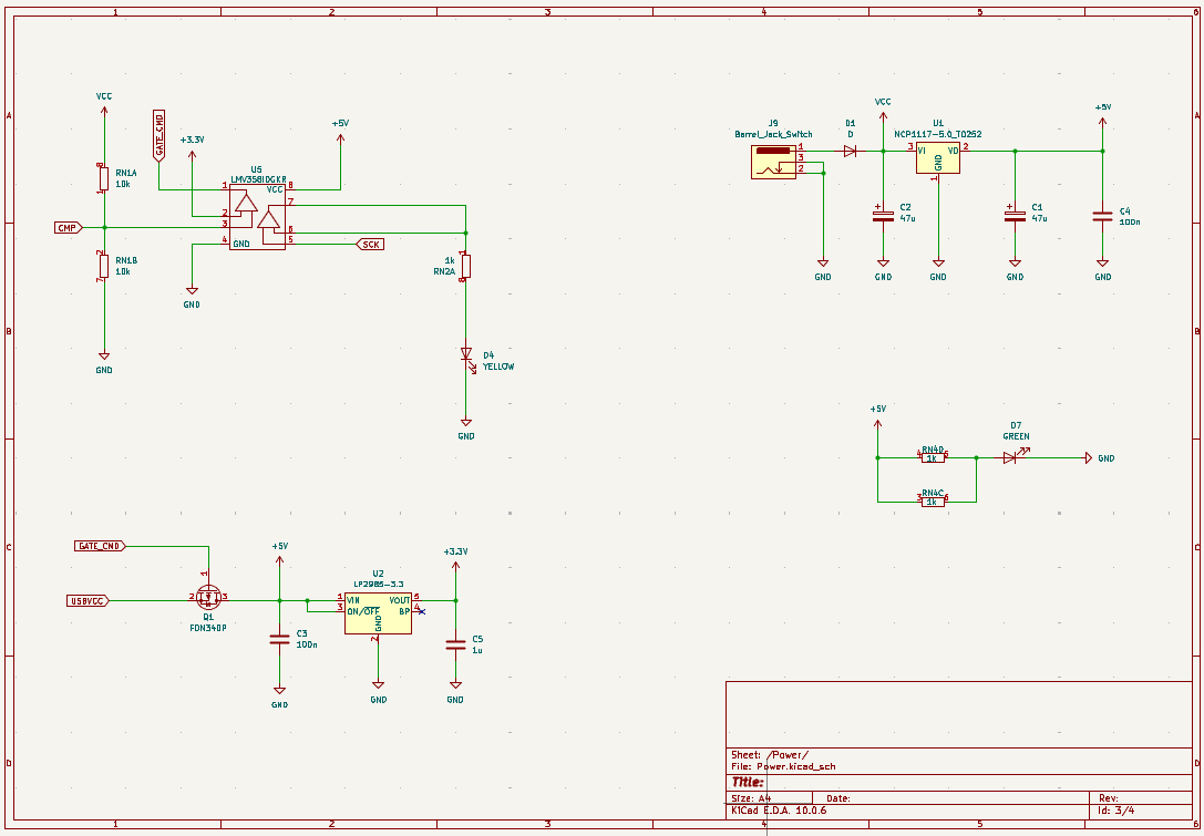
| Qty | Value | Footprint | References |
|---|---|---|---|
| 7 | 100n | Capacitor_SMD:C_0603_1608Metric | C3, C4, C6, C7, C8, C9, C12 |
| 3 | Fiducial | Fiducial:Fiducial_1mm_Mask3mm | FID1, FID2, FID3 |
| 3 | YELLOW | LED_SMD:LED_0805_2012Metric | D4, D5, D6 |
| 2 | 1M | Resistor_SMD:R_0603_1608Metric | R1, R2 |
| 2 | 1k | Resistor_SMD:R_Array_Convex_4x0603 | RN2, RN4 |
| 2 | 1u | Capacitor_SMD:C_0603_1608Metric | C5, C10 |
| 2 | 22p | Capacitor_SMD:C_0603_1608Metric | C11, C13 |
| 2 | 47u | Capacitor_SMD:CP_Elec_5x5.4 | C1, C2 |
| 2 | 5k1 | Resistor_SMD:R_0603_1608Metric | R3, R4 |
| 2 | 5pF@1MHz | Resistor_SMD:R_0603_1608Metric | Z1, Z2 |
| 2 | Conn_01x08 | Connector_PinSocket_2.54mm:PinSocket_1x08_P2.54mm_Vertical | J5, J7 |
| 2 | Conn_02x03_Odd_Even | Connector_PinHeader_2.54mm:PinHeader_2x03_P2.54mm_Vertical | J1, J3 |
| 2 | D | Diode_SMD:D_1206_3216Metric | D2, D3 |
| 2 | SolderJumper_2_Open | Jumper:SolderJumper-2_P1.3mm_Open_Pad1.0x1.5mm | JP1, JP2 |
| 1 | 10k | Resistor_SMD:R_Array_Convex_4x0603 | RN1 |
| 1 | 1kohm@100MHz | Inductor_SMD:L_0805_2012Metric | FB1 |
| 1 | 22R | Resistor_SMD:R_Array_Convex_4x0603 | RN3 |
| 1 | ATmega16U2-MU | Package_DFN_QFN:VQFN-32-1EP_5x5mm_P0.5mm_EP3.1x3.1mm | U3 |
| 1 | ATmega328P-P | Package_DIP:DIP-28_W7.62mm_Socket | U4 |
| 1 | Barrel_Jack_Switch | Connector_BarrelJack:BarrelJack_Kycon_KLDX-0202-xC_Horizontal | J9 |
| 1 | Conn_01x06 | Connector_PinSocket_2.54mm:PinSocket_1x06_P2.54mm_Vertical | J6 |
| 1 | Conn_01x10 | Connector_PinSocket_2.54mm:PinSocket_1x10_P2.54mm_Vertical | J4 |
| 1 | Conn_02x02_Odd_Even | Extra:02x02 tht hole | J2 |
| 1 | Crystal | Crystal:Crystal_HC49-4H_Vertical | Y2 |
| 1 | Crystal_GND2 | Crystal:Resonator_SMD_Murata_CSTxExxV-3Pin_3.0x1.1mm | Y1 |
| 1 | D | Diode_SMD:D_SMB | D1 |
| 1 | FDN340P | Package_TO_SOT_SMD:SC-59 | Q1 |
| 1 | FerriteBead | Inductor_SMD:L_0805_2012Metric | FB2 |
| 1 | GREEN | LED_SMD:LED_0805_2012Metric | D7 |
| 1 | LMV358IDGKR | Package_SO:MSOP-8_3x3mm_P0.65mm | U5 |
| 1 | LP2985-3.3 | Package_TO_SOT_SMD:SOT-23-5 | U2 |
| 1 | NCP1117-5.0_TO252 | Package_TO_SOT_SMD:SOT-223-3_TabPin2 | U1 |
| 1 | Polyfuse | Fuse:Fuse_1812_4532Metric_Pad1.30x3.40mm_HandSolder | F2 |
| 1 | SW_Push_Open_Dual | Button_Switch_SMD:SW_SPST_B3S-1000 | SW1 |
| 1 | USB_C_Receptacle_USB2.0_16P | Connector_USB:USB_C_Receptacle_GCT_USB4105-xx-A_16P_TopMnt_Horizontal | J8 |

bostang/PCBs
My repository for documenting all PCB Projects I have done

kaustubh850/ArduinoEquipped
A Repo wit Arduino Uno Compatible Boards with on-board Addons.


izunduprince1-design/ARDRUINO-UNO-BOARD
ARDRUINO UNO BUILT PCB BORD
It measures 67.8 × 56 mm and has 2 copper layers, 1.6 mm thick.
56 parts, built around the ATMEGA16U2-MU, ATMEGA328P-PU, LMV358IDGKR and LP2985-33DBV. The full list of its parts is on this page, with links to each part's symbol and footprint where PCBKit's library has them.
From the aarthirethinabala/Arduino-Uno-Compatible-PCB repository on GitHub, at the commit this page was made from: the board is Arduino.kicad_pcb and its schematic ATMEGA328P-PU.kicad_sch. PCBKit opens the board in the browser, with nothing to install.
Its repository states no licence, so its author keeps all rights: ask aarthirethinabala before reusing the design.