
2 layers232 × 110 mm
Relay8
YORROY123/kicad-scripted-pcb
Three KiCad 10 PCBs designed entirely as Python code with layered verification
65 parts1MIT

Three KiCad 10 PCBs designed entirely as Python code with layered verification
Cm5 is an open-source printed circuit board by YORROY123, from the YORROY123/kicad-scripted-pcb repository on GitHub, published under the MIT licence. It is a 4-layer board of 170 × 120 mm with 243 parts on 360 nets, routed with 1,695 tracks and 524 vias.
It is built around the IP804AR, LAN7800/Y9X and TPS568230RJER, with the AP2171WG, FSUSB42MUX and TPS2051CDBV among its other parts. Its parts include 129 capacitors, 52 resistors, 12 diodes, 11 ICs and 10 connectors. It belongs with the computers and single-board computers boards and the ESP32, RISC-V and Raspberry Pi (Linux) boards of this library.


Three KiCad 10 boards designed entirely as code: Python scripts produce the schematic, the PCB placement, the routing (via freerouting) and the copper pours, and each board rebuilds from scratch with one command. The KiCad GUI is never opened.
The point is verification. Every build runs several independent checks, because each one is blind to errors the others catch. Some of those errors turned up while these boards were being built and are listed below.
| Board | Result | |
|---|---|---|
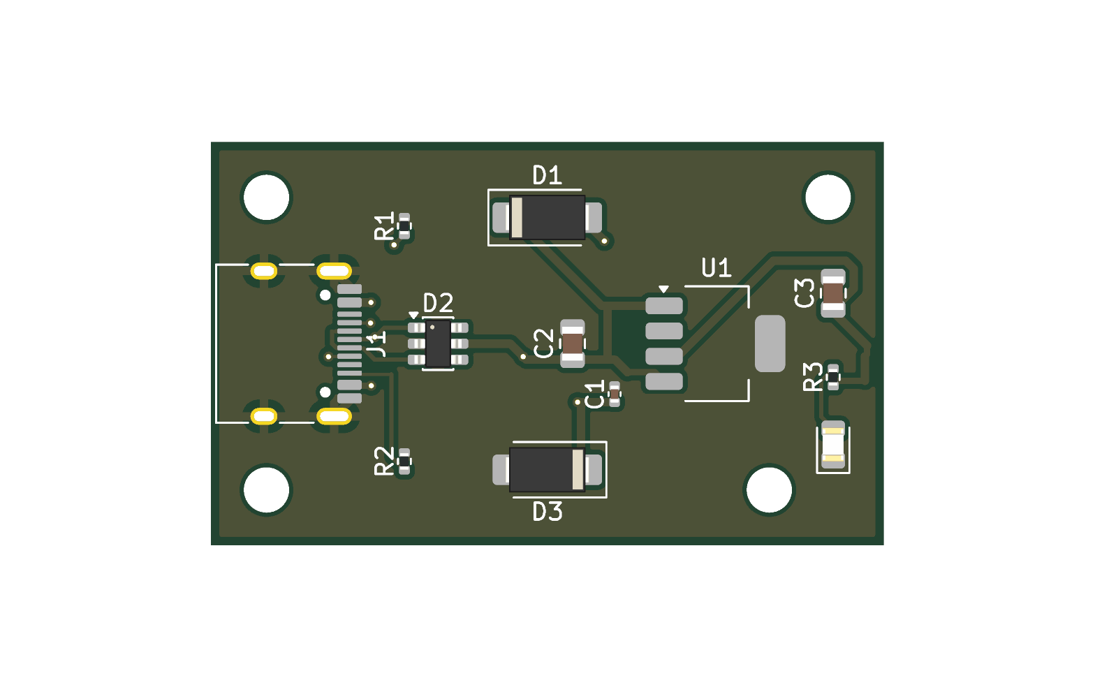 | usbc-ldo: USB-C 5 V → 3.3 V LDO → LED. 40 × 24 mm, 2 layers. Includes an ngspice power-path simulation. | ERC 0, DRC 0, schematic parity |
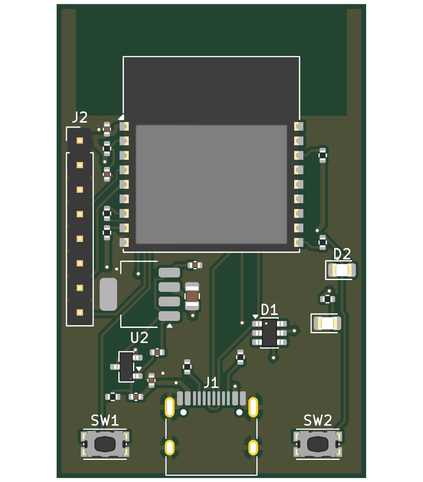 | esp32c3: ESP32-C3 minimal board with native USB, LP38693 LDO, RESET/BOOT, LEDs and an 8-pin header. 32 × 49 mm. | ERC 0, DRC 0, schematic parity, pin-by-pin netlist check |
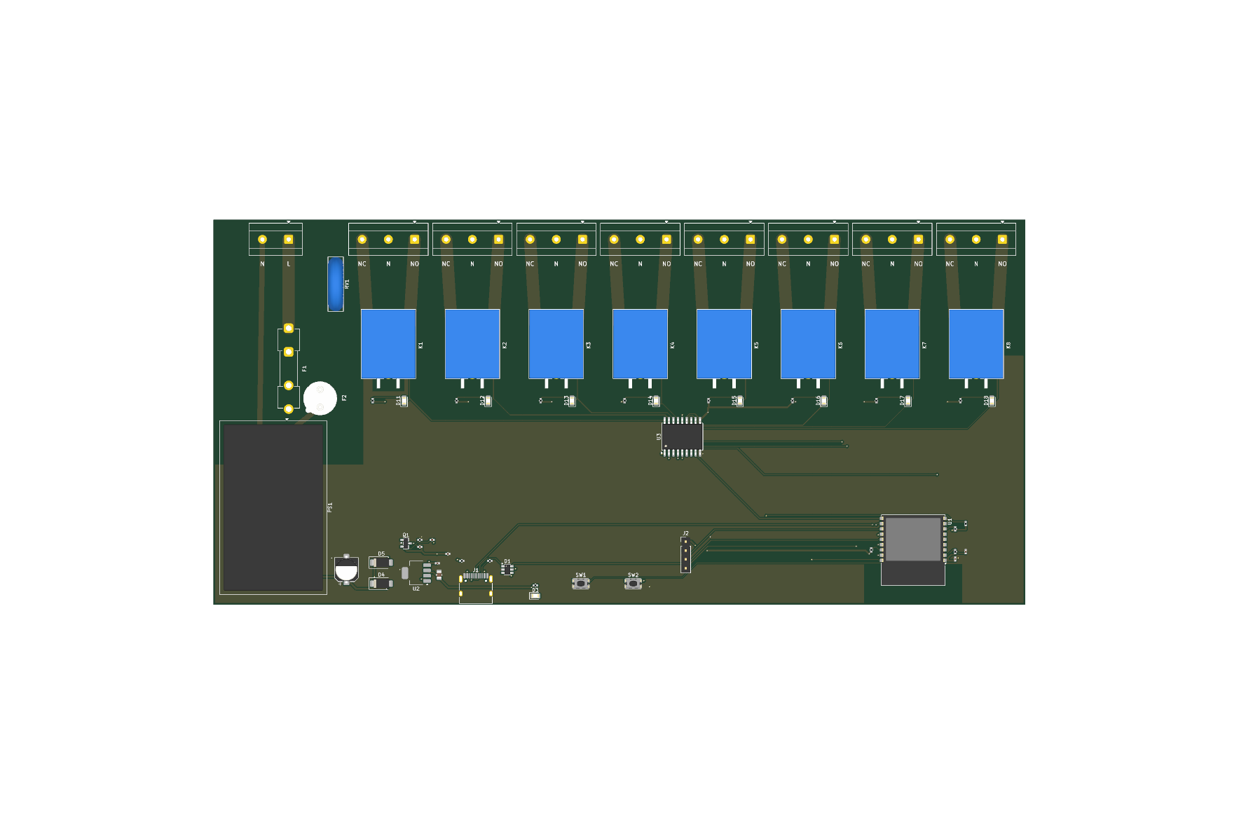 | relay8: ESP32-C3 + ULN2803 driving 8 mains relays from one mains cable: on-board HLK-10M05 AC-DC (100–240 VAC), T8A fuse, varistor, L/N bus traces, per-channel NO · N · NC terminals, isolation slots and custom mains clearance rules. 232 × 110 mm. Not safety-certified. | ERC 0, DRC errors 0 (40 silkscreen-clipped-by-slot/edge warnings listed), schematic parity |
Each ESP32 board has a FIRMWARE.md with the pin map, flashing steps, a first program, and, for
relay8, the mains wiring.
gen/board.py ──► .kicad_sch ──► ERC ──► netlist ──► netlist check (vs expected_nets.json)
                                                     │
                                                     ▼
                                     design review (lib/review.py, datasheet rules)
                                                     │
gen/pcb.py ◄─────────────────────────────────────────┘   place footprints, board outline,
   │                                                     net classes, placement self-check
   ▼
.kicad_pcb ──► Specctra DSN ──► freerouting ──► SES ──► import + GND pour ──► DRC (+ schematic parity)
                                                                                   │
                     lcsc.json ──► lib/lcsc.py (online, run by hand) ──► lcsc-check.json
                                                                                   │
                                                       lib/fab.py ◄────────────────┘
                                     Gerber + drill zip, JLCPCB BOM / CPL, hand-solder list
Every step stops the build on failure; nothing is passed downstream with a known error.
kicad-cli has no "update PCB from schematic" command, so lib/pcbgen.py builds the board from
the exported netlist with pcbnew.
| Check | Catches | Missed here (caught by something else) |
|---|---|---|
schgen.crossing_pins() / overlapping_wires() | a wire running across a pin (silent short), two nets merged by overlapping wires | — |
| KiCad ERC | unconnected pins, undriven power | LED wired backwards (two passive pins, ERC is fine with it). Found by reading the netlist while building the PCB. |
check_netlist.py vs expected_nets.json | wrong pin→net, single-pin nets | ERC ignores "global label appears only once" by default, so a label typo creates an isolated net with no ERC error. Proven with a deliberate typo (mutation test). |
| placement self-check | pad nets vs netlist, footprints off-board, courtyard overlap | Uses real courtyard polygons. The ESP32 module's courtyard is T-shaped, and bounding boxes reject legal positions. |
DRC + --schematic-parity | clearance, track width, edge clearance, schematic vs PCB | — |
custom DRC rules (relay8.kicad_dru) | mains ↔ low voltage ≥ 3.0 mm, mains ↔ mains ≥ 2.4 mm | Creepage around the slots is not checked by DRC. Needs a human. |
ngspice simulation (usbc-ldo/sim) | design margins | The first board's 1.1 V-dropout LDO falls out of regulation at USB's 4.40 V minimum, and its input capacitance injects ~124 µC on hot-plug (USB 2.0 limit: 50 µC). All three boards now use LP38693 (12 V input rating): esp32c3/sim showed that with only 1 µF on VBUS, hot-plug cable ringing reaches 7.7–8.6 V, above the 6.5 V rating of the AP2112K the ESP32 boards first used. |
lib/review.py design review (datasheet rules on the netlist) | wrong intent: diode/TVS polarity, LED current from the real Vf range, decoupling and rail ranges per datasheet, USB-C CC pull-downs, ESP32-C3 EN RC / strapping pins / GPIO18-19, relay flyback path and pickup voltage, capacitor voltage and polarity, per-supply current budget, LDO junction temperature, USB VBUS capacitance | usbc-ldo's SMAJ5.0A TVS was wired backwards: anode on +5 V, cathode on GND, a short the moment USB is plugged in. KiCad's symbol names the cathode pin "A1". ERC, DRC, the netlist check and the SPICE model (which had it the right way round) all passed. It also found a blue LED on a 3.3 V GPIO (Vf up to 3.6 V) and green power LEDs at ~0.45 mA. lib/review_test.py breaks the real netlists 20 ways and expects each rule to fire. |
lib/lcsc.py + lib/fab.py | LCSC part number vs model, stock, package size, R/C value, LED colour; symbol default footprint vs assigned footprint; drill count; BOM/CPL/board refdes | All three boards used the USBLC6-2P6 symbol (SOT-666) on a SOT-23-6 footprint: same pinout, so nothing else noticed, but a BOM by value buys parts that do not fit. The SMAJ5.0A part number first chosen had zero stock. |
--router.automatic_neckdown=false --router.neck_width_um=150.--router.copper_to_edge_clearance_um. That setting does not cover internal slots, so put keepouts around slots..kicad_pro, not .kicad_pcb. Save with pcbnew.SaveBoard(), which writes both.board.Remove(zone) from Python can raise 'SwigPyObject' has no attribute 'thisown' or crash pcbnew (0xC0000005). Use board.Delete().specctra_export.cpp) by the arc-approximation margin.KICAD_BIN / KICAD_SHARE if it is not in the default location.numpy, scipy and matplotlib.lib/lcsc.py (JLCPCB parts API). The build itself runs offline.tools\setup-tools.ps1 once; it downloads both into tools\ with pinned SHA-256 checks.powershell -ExecutionPolicy Bypass -File tools\setup-tools.ps1
powershell -ExecutionPolicy Bypass -File boards\esp32c3\build.ps1
python lib\review_test.py # design-review mutation tests; needs the boards built onceThe build ends with boards/<b>/fab/:
| File | Use |
|---|---|
<b>-gerber.zip | upload to JLCPCB as the PCB |
<b>-bom.csv, <b>-cpl.csv | upload for SMT assembly (parts LCSC can supply) |
hand-solder.csv | parts LCSC cannot supply (relay8: mains terminals, fuse holders) |
rotation-review.csv | every part's CPL rotation and where it came from. None is hardware-verified: compare each part in JLCPCB's placement preview |
Also written to boards/<b>/: review.txt (design review, including the inferred net voltages) and
lcsc-check.json (part numbers as checked against JLCPCB, with stock and attributes).
lib/schgen.py, ksym.py, netlabel.py   schematic writer (symbols flattened from the KiCad library)
lib/check_netlist.py                  netlist vs expected_nets.json
lib/review.py, review_test.py         design review rules + mutation tests
lib/pcbgen.py, route.py               PCB builder (BoardSpec), freerouting round trip, GND pour
lib/lcsc.py, fab.py, jlc_rotations.json   part-number check, fabrication outputs
lib/field2d.py, field2d_check.py      2-D field solver for trace impedance + validation
boards/<b>/gen/board.py   the circuit (pin -> net table)
boards/<b>/gen/pcb.py     placement (BoardSpec)
boards/<b>/lcsc.json      hand-written LCSC part numbers ("value|footprint" -> part)
boards/<b>/review-waivers.json   accepted review findings, each with a reason
boards/<b>/build.ps1      one-command build
boards/<b>/sim/           ngspice and field-solver studies
tools/      setup-tools.ps1 (downloads are git-ignored)
Want to add a board or a review rule? See CONTRIBUTING.md.
Code comments are in Chinese. The boards were built while comparing AI-assisted workflows in KiCad and EasyEDA Pro.
These are two-layer boards with modules and simple power. There is no controlled-impedance routing,
no length matching, no BGA and no SI/PI analysis; freerouting does none of these (lib/field2d.py
can tell you whether a trace needs it). The fabrication files are complete enough to order, but
nobody has built these boards yet: CPL rotations are unverified and the design review is a set of
rules, not an engineer. Have a person review before ordering. This applies above all to
relay8, which switches mains voltage.
MIT. freerouting (GPL-3.0) and the Temurin JRE (GPL-2.0 with Classpath Exception) are downloaded at setup time and are not part of this repository.
| Qty | Value | Footprint | References |
|---|---|---|---|
| 70 | 100nF | Capacitor_SMD:C_0402_1005Metric | C101, C102, C103, C104, C106, C107, C108, C109, C111, C112, C113, C114, C115, C120, C121, C131 +54 |
| 16 | 10k | Resistor_SMD:R_0402_1005Metric | R18, R74, R75, R76, R77, R78, R102, R103, R132, R133, R205, R206, R207, R208, R209, R230 |
| 14 | 47uF | Capacitor_SMD:C_1210_3225Metric | C30, C31, C32, C33, C34, C40, C41, C42, C43, C45, C46, C50, C220, C221 |
| 7 | 1uF | Capacitor_SMD:C_0402_1005Metric | C48, C105, C117, C135, C147, C210, C213 |
| 6 | 4.7uF | Capacitor_SMD:C_1210_3225Metric | C11, C12, C13, C14, C15, C16 |
| 6 | 470 | Resistor_SMD:R_0402_1005Metric | R60, R61, R104, R105, R134, R135 |
| 5 | 4.7uF | Capacitor_SMD:C_0603_1608Metric | C84, C85, C86, C87, C201 |
| 4 | 100k | Resistor_SMD:R_0402_1005Metric | R25, R202, R203, R204 |
| 4 | 10uF | Capacitor_SMD:C_0805_2012Metric | C100, C110, C130, C140 |
| 4 | 27pF | Capacitor_SMD:C_0402_1005Metric | C118, C119, C148, C149 |
| 4 | 75 | Resistor_SMD:R_0603_1608Metric | R80, R81, R82, R83 |
| 4 | MountingHole_2.7mm_M2.5 | MountingHole:MountingHole_2.7mm_M2.5 | H5, H6, H7, H8 |
| 4 | MountingHole_3.2mm_M3 | MountingHole:MountingHole_3.2mm_M3 | H1, H2, H3, H4 |
| 3 | 12k | Resistor_SMD:R_0402_1005Metric | R101, R131, R210 |
| 3 | 5.1k | Resistor_SMD:R_0402_1005Metric | R24, R200, R201 |
| 3 | GREEN | LED_SMD:LED_0805_2012Metric | D40, D42, D51 |
| 3 | SM6T68A | Diode_SMD:D_SMB | D20, D60, D61 |
| 3 | USBLC6-2SC6 | Package_TO_SOT_SMD:SOT-23-6 | D70, D71, D72 |
| 2 | 1.5A | Fuse:Fuse_1206_3216Metric | F40, F41 |
| 2 | 100nF | Capacitor_SMD:C_0805_2012Metric | C92, C93 |
| 2 | 100uF | Capacitor_SMD:CP_Elec_6.3x7.7 | C211, C214 |
| 2 | 1k | Resistor_SMD:R_0402_1005Metric | R50, R51 |
| 2 | 1nF 2kV | Capacitor_SMD:C_1206_3216Metric | C90, C91 |
| 2 | 22pF | Capacitor_SMD:C_0402_1005Metric | C208, C209 |
| 2 | 25MHz | Crystal:Crystal_SMD_3225-4Pin_3.2x2.5mm | Y40, Y41 |
| 2 | 2k | Resistor_SMD:R_0402_1005Metric | R100, R130 |
| 2 | 3.3uH | Inductor_SMD:L_1008_2520Metric | L40, L41 |
| 2 | AP2171W | Package_TO_SOT_SMD:SOT-23-5 | U62, U63 |
| 2 | G2423S | CM5:Transformer_CNDtek_G2423S | T40, T41 |
| 2 | LAN7800/Y9X | Package_DFN_QFN:QFN-48-1EP_7x7mm_P0.5mm_EP5.3x5.3mm | U40, U41 |
| 2 | TPD4EUSB30 | Package_SON:USON-10_2.5x1.0mm_P0.5mm | U30, U31 |
| 2 | YELLOW | LED_SMD:LED_0805_2012Metric | D41, D43 |
| 1 | 1.5uH IHLP4040 | Inductor_SMD:L_Vishay_IHLP-4040 | L20 |
| 1 | 100nF | Capacitor_SMD:C_0603_1608Metric | C17 |
| 1 | 100pF | Capacitor_SMD:C_0402_1005Metric | C44 |
| 1 | 100uF | Capacitor_THT:CP_Radial_D12.5mm_P5.00mm | C10 |
| 1 | 12.4k | Resistor_SMD:R_0402_1005Metric | R11 |
| 1 | 150 | Resistor_SMD:R_0402_1005Metric | R17 |
| 1 | 150pF | Capacitor_SMD:C_0402_1005Metric | C23 |
| 1 | 15pF | Capacitor_SMD:C_0402_1005Metric | C19 |
| 1 | 1M | Resistor_SMD:R_0402_1005Metric | R211 |
| 1 | 1uF | Capacitor_SMD:C_1206_3216Metric | C82 |
| 1 | 2.2uF | Capacitor_SMD:C_0603_1608Metric | C20 |
| 1 | 20k | Resistor_SMD:R_0402_1005Metric | R22 |
| 1 | 23.2k | Resistor_SMD:R_0402_1005Metric | R14 |
| 1 | 24MHz | Crystal:Crystal_SMD_2520-4Pin_2.5x2.0mm | Y60 |
| 1 | 3.3uH SPM10065VT | Inductor_SMD:L_Bourns_SRP1050WA | L10 |
| 1 | 33.2k | Resistor_SMD:R_0402_1005Metric | R12 |
| 1 | 330k | Resistor_SMD:R_0402_1005Metric | R23 |
| 1 | 4.42k | Resistor_SMD:R_0402_1005Metric | R15 |
| 1 | 402k | Resistor_SMD:R_0805_2012Metric | R10 |
| 1 | 412 | Resistor_SMD:R_0805_2012Metric | R13 |
| 1 | 47nF | Capacitor_SMD:C_0402_1005Metric | C18 |
| 1 | 47uF | Capacitor_SMD:CP_Elec_10x10 | C83 |
| 1 | 4A 63V | Fuse:Fuse_1206_3216Metric | F1 |
| 1 | 54V IN | TerminalBlock_Phoenix:TerminalBlock_Phoenix_MKDS-1,5-2-5.08_1x02_P5.08mm_Horizontal | J20 |
| 1 | 6.8nF | Capacitor_SMD:C_0402_1005Metric | C22 |
| 1 | 7.5k | Resistor_SMD:R_0402_1005Metric | R16 |
| 1 | 820pF | Capacitor_SMD:C_0402_1005Metric | C24 |
| 1 | 91k | Resistor_SMD:R_0402_1005Metric | R21 |
| 1 | BSC070N10NS5 | Package_TO_SOT_SMD:TDSON-8-1 | Q11 |
| 1 | BSC160N10NS3G | Package_TO_SOT_SMD:TDSON-8-1 | Q10 |
| 1 | CM5 pins 1-100 | CM5:Amphenol_10164227-1001A1RLF_2x50_P0.4mm | J1 |
| 1 | CM5 pins 101-200 | CM5:Amphenol_10164227-1001A1RLF_2x50_P0.4mm | J2 |
| 1 | CR2032 | Battery:BatteryHolder_Keystone_3034_1x20mm | BT50 |
| 1 | FAN | Connector_JST:JST_SH_SM04B-SRSS-TB_1x04-1MP_P1.00mm_Horizontal | J81 |
| 1 | FLASH/RUN | Button_Switch_SMD:SW_SPDT_PCM12 | SW51 |
| 1 | FSUSB42MUX | Package_SO:MSOP-10_3x3mm_P0.5mm | U60 |
| 1 | GPIO 40-pin | Connector_PinHeader_2.54mm:PinHeader_2x20_P2.54mm_Vertical | J80 |
| 1 | HDMI | Connector_Video:HDMI_A_Molex_208658-1001_Horizontal | J70 |
| 1 | HR911130A | CM5:RJ45_Hanrun_HR911130A_Horizontal | J30 |
| 1 | IP804AR | Package_DFN_QFN:QFN-48-1EP_7x7mm_P0.5mm_EP5.3x5.3mm | U50 |
| 1 | LM5146RGYR | Package_DFN_QFN:Texas_RGY_R-PVQFN-N20_EP2.05x3.05mm | U10 |
| 1 | M.2 M-key | CM5:M.2_Socket_M_TE_1-2199230-6 | J60 |
| 1 | POE0 | Connector_RJ:RJ45_Amphenol_RJHSE5380 | J40 |
| 1 | POE1 | Connector_RJ:RJ45_Amphenol_RJHSE5380 | J41 |
| 1 | POWER | Button_Switch_SMD:SW_Push_1P1T_NO_CK_KMR2 | SW50 |
| 1 | RED | LED_SMD:LED_0805_2012Metric | D50 |
| 1 | TPS2051CDBV | Package_TO_SOT_SMD:SOT-23-5 | U70 |
| 1 | TPS568230RJER | Package_DFN_QFN:Texas_RJE0020A_VQFN-20-1EP_3x3mm_P0.45mm_EP0.675x0.76mm | U20 |
The 239 most common of 243 parts.
YORROY123/kicad-scripted-pcb
Three KiCad 10 PCBs designed entirely as Python code with layered verification

YORROY123/kicad-scripted-pcb
Three KiCad 10 PCBs designed entirely as Python code with layered verification

YORROY123/kicad-scripted-pcb
Three KiCad 10 PCBs designed entirely as Python code with layered verification

JayTzw/Mechanical---Robotics---Electronics
CAD files, Circuit schematics & PCB designs, Robotics simulations

PaulBichl/vibepcb-smu
VibePCB example: 4-quadrant SMU (+-30 V / +-1 A, USB-C PD, Ethernet) designed with an LLM

murexrobotics/electrical
Highly integrated electronics design and printed circuit boards (PCBs) for the MATE ROV Competition. Attempt the impossible.


dremeier/Arduino-JK-BMS-To-Pylontech-CAN-PCB
PCB and Case for the Arduino JK-BMS To Pylontech CAN converter


flannellab/AI_Design_Generation
Collection of things for AI generation of PCB designs (Components, Schematics, PCBs, Docs)

izzeldeenakloub/Gigabit-Ethernet-to-USB-C-Adapter
A KiCad design project for a USB-C to Gigabit Ethernet adapter and my first complete 4-layer PCB layout.
It measures 170 × 120 mm and has 4 copper layers, 1.6 mm thick.
243 parts, built around the IP804AR, LAN7800/Y9X, TPS568230RJER and AP2171WG. The full list of its parts is on this page, with links to each part's symbol and footprint where PCBKit's library has them.
From the YORROY123/kicad-scripted-pcb repository on GitHub, at the commit this page was made from: the board is boards/cm5/cm5.kicad_pcb and its schematic boards/cm5/cm5.kicad_sch. PCBKit opens the board in the browser, with nothing to install.
Its repository publishes it under the MIT licence: you may reuse it on that licence's terms (keep the author's notice, and for a copyleft licence share your changes alike).