2 layers90 × 38 mm
LCD OLinuXino-5TS Rev.B
OLIMEX/OLINUXINO
OLINUXINO is Open Source / Open Hardware, low cost from EUR 24 Linux Industrial grade Single Board Computer capable to operate -25+85C
56 parts1.5k

 ThePurox/zplitzalp9
The Zplitzalp is a split, wireless, ultra-low-profile version of kilipan's Zilpzalp. The required Switches are the Cherry ultra low profile switches. The footprint is based on the ones found here.
Zplitzalp is an open-source printed circuit board by ThePurox, from the ThePurox/zplitzalp repository on GitHub. It is a 2-layer board of 139.8 × 157.1 mm with 56 parts on 69 nets, routed with 832 tracks and 45 vias.
Its parts include 32 switches, 14 diodes and 2 ICs. It belongs with the nRF52 and nRF5x boards of this library.
The Zplitzalp is a split, wireless, ultra-low-profile version of kilipan's Zilpzalp. The required Switches are the Cherry ultra low profile switches. The footprint is based on the ones found here.
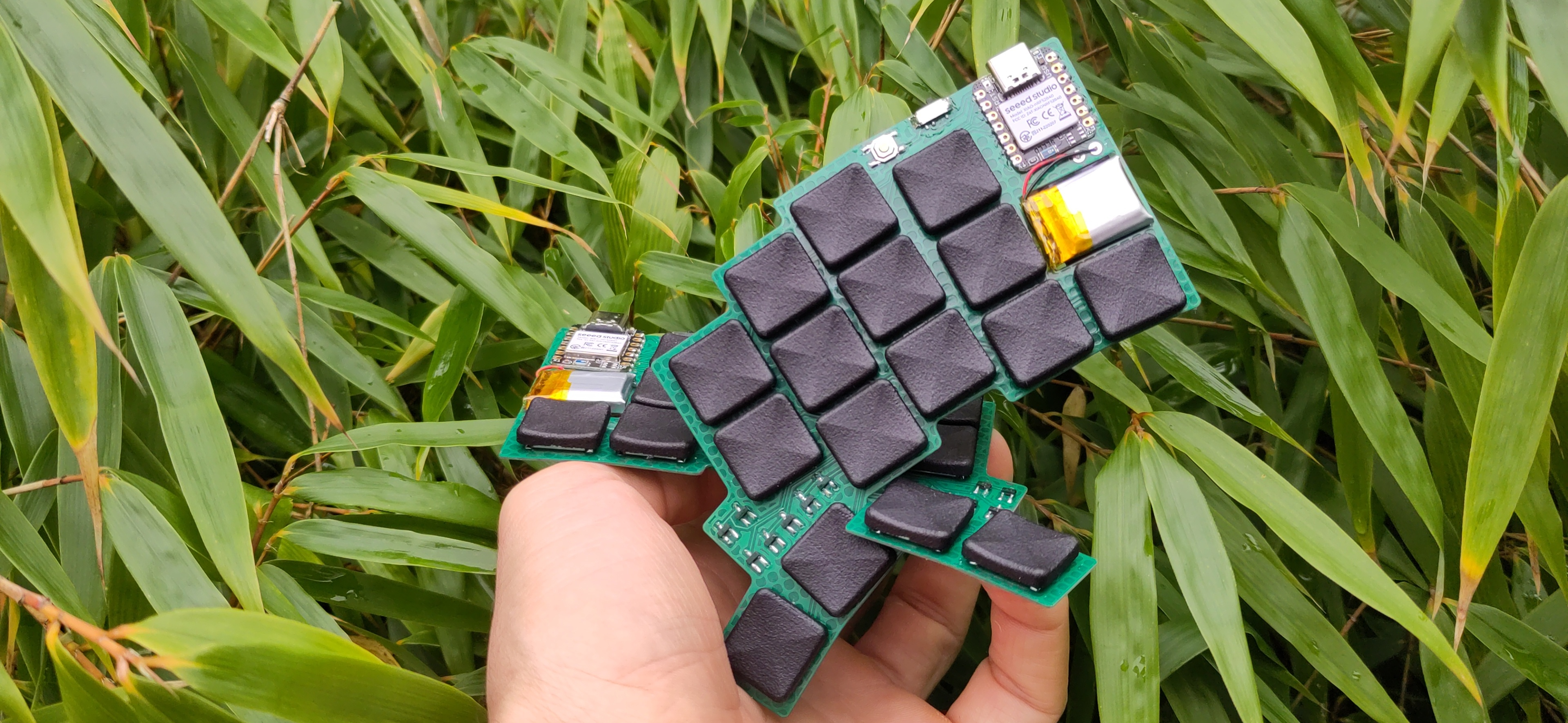
The soldering of the switches has to be done with care. I recommend to solder the switches by hand with a soldering iron, do not use a small hotplate. If you use a hotplate the thin PCB will bend due to the combination of thermal expansion of the board and the board being warmer on the side of the hotplate. As it cools down the solder solidifies and the switch will hold the PCB in its bend shape. I like to solder them by placing the switch on the PCB and soldering at least one of the accessible solder pads from the front. Then turn the PCB around such that you can see the "Zplitzalp"-text and solder the remaining pads from the bottom. Solder the pads on the PCB as well as the ones through the cutout. Be careful not to use to much solder when soldering the pads of the switches. If you use too much solder the switch will not work anymore. Try with one and see whether it still works before soldering in all the switches and potentially ruining all your switches.
A 20x15x5mm battery fits into the cutout. Solder its positive side (red wire) to the pad with the + next to it. The negative side of the battery (black wire) needs to be soldered to the pad with the - sign.
Solder the XIAO BLE to the boards. Do not forget the pads on the backside. These need to be soldered through the cutout, just as you did for the switches.
The last things to solder are 2 MSK12C02 on-off switches, 2 5.1x5.1mm reset buttons and 14 BAV70 diodes.
Now it is time to install keycaps. You can get them printed at JLC3DP for relatively little money. You find the required files in fookers mnhTTn repository.
| component | number required |
|---|---|
| Cherry ultra low profile switches | 28 |
| Keycaps for the switches | 28 |
| XIAO BLE | 2 |
| MSK12C02 on-off switches | 2 |
| 5.1x5.1mm reset buttons | 2 |
| BAV70 diodes | 14 |
| 20x15x5mm battery | 2 |
| Qty | Value | Footprint | References |
|---|---|---|---|
| 28 | SW_Push | Cherry_ULP:Cherry_ULP_TH_CUT | SW1, SW2, SW10, SW11, SW12, SW13, SW14, SW15, SW16, SW17, SW18, SW19, SW20, SW21, SW22, SW23 +12 |
| 14 | BAV70_Small | BeiBob:SOT-23_Handsoldering | D01, D02, D03, D04, D05, D06, D07, D08, D09, D10, D11, D12, D13, D14 |
| 2 | + | mnhttn:BatteryPad | BAT+1, BAT+2 |
| 2 | - | mnhttn:BatteryPad | BAT-1, BAT-2 |
| 2 | G*** | kibuzzard-672142E0 | kibuzzard-672142E0, kibuzzard-672142E0 |
| 2 | G*** | kibuzzard-67214396 | kibuzzard-67214396, kibuzzard-67214396 |
| 2 | SW_Push | mnhttn:PushSwitch | SW31, SW32 |
| 2 | SW_SPDT | mnhttn:MSK12C02 | SW29, SW30 |
| 2 | Seeeduino Xiao nRF52840 | xiao:xiao-ble-smd-cutout-extra-pins | U1, U2 |
OLIMEX/OLINUXINO
OLINUXINO is Open Source / Open Hardware, low cost from EUR 24 Linux Industrial grade Single Board Computer capable to operate -25+85C

hackclub/OnBoard
💡 Join 1,000 teenagers and make your first PCB with a $100 grant!


GEIGEIGEIST/KLOTZ
KLOTZ is 34 keys column-staggered split keyboard. It uses an encoder and three status LEDs on each side.

ergonautkb/one
Ergonaut One is an open-source ergonomic wireless split mechanical keyboard designed by Ergonaut Keyboards.

matthewcieplak/super-sixteen
Code and schematics for the Super Sixteen Eurorack sequencer

EnriqueNeyra/Aeroq
An Indoor Air Quality Monitor Powered by ESP32, SCD40, and SEN54
It measures 139.8 × 157.1 mm and has 2 copper layers, 1.6 mm thick.
56 parts. The full list of its parts is on this page, with links to each part's symbol and footprint where PCBKit's library has them.
From the ThePurox/zplitzalp repository on GitHub, at the commit this page was made from: the board is zplitzalp.kicad_pcb and its schematic zplitzalp.kicad_sch. PCBKit opens the board in the browser, with nothing to install.
Its repository states no licence, so its author keeps all rights: ask ThePurox before reusing the design.