
4 layers100 × 100 mm
LM399-Voltage Standard
IndexAsm/LM399-Voltage-Standard
10V Voltage Standard used to calibrate equipment.
118 parts

 TU-Darmstadt-APQ/Voltage_reference6
LM399/ADR1399 based 10 V/15 V sub-ppm stable reference
Reference board is an open-source printed circuit board by TU-Darmstadt-APQ, from the TU-Darmstadt-APQ/Voltage_reference repository on GitHub, published under the CERN-OHL-W-2.0 licence. It is a 2-layer board of 34 × 25 mm with 21 parts on 20 nets, routed with 182 tracks and 5 vias.
It is built around the LT1001CD, TMP236EVM and BAS116. Its parts include 6 capacitors, 3 ICs, 2 resistors, 1 diode and 1 connector.


This repository contains the KiCAD PCB project files for a sub-ppm temperature coefficient negative voltage reference used in the digital laser driver design.
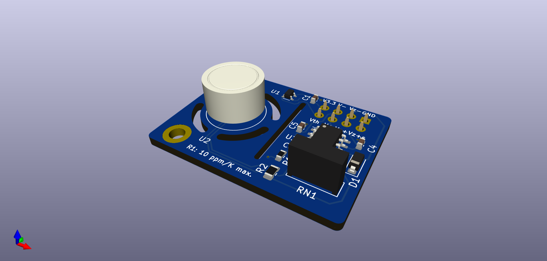
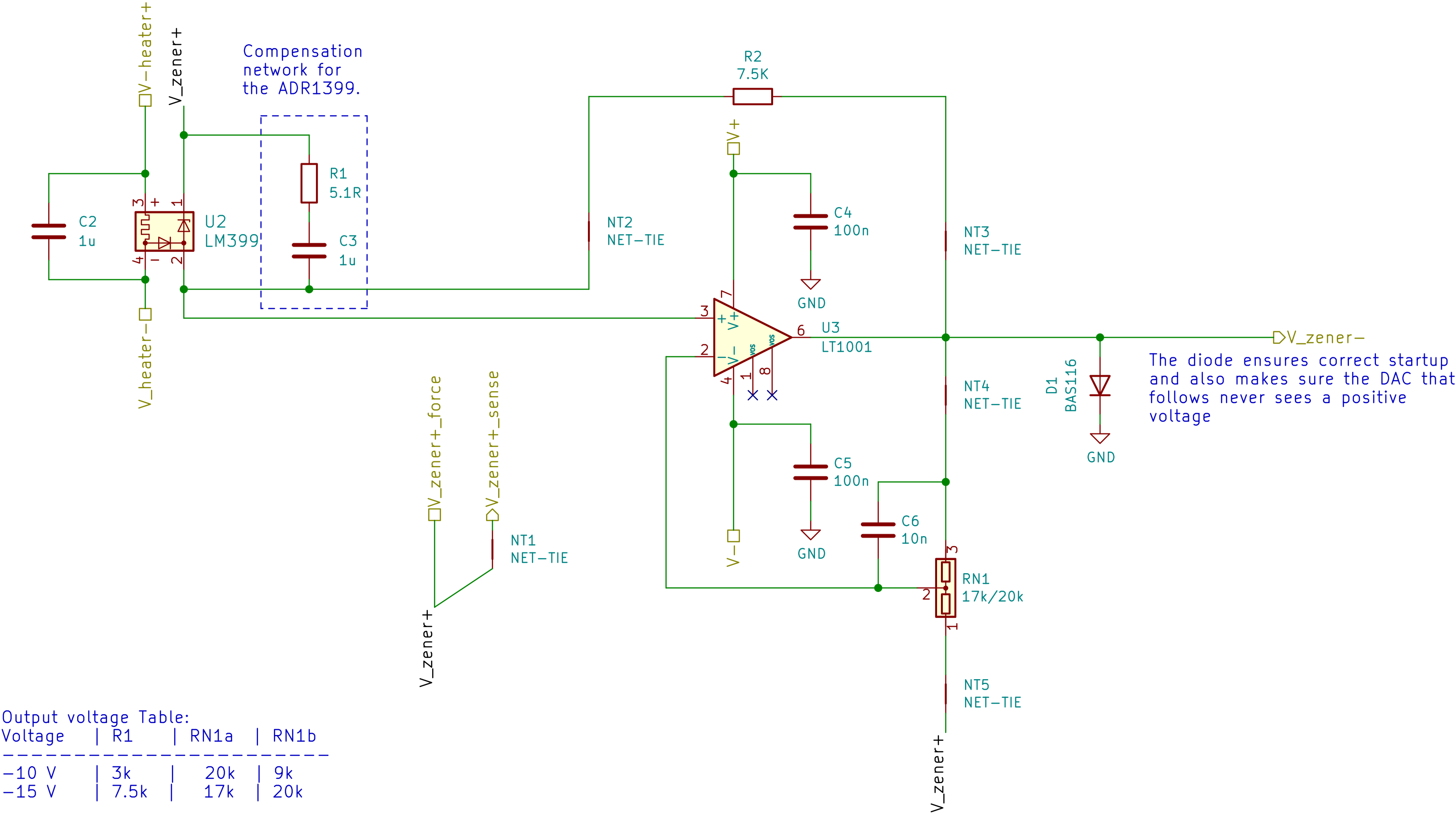
This circuit utilizes the excellent LM399 voltage reference and outputs an amplified voltage of either -10 V or -15 V. There is no option to trim the output voltage as the absolute value is not that important, but stability is. The output voltage will be 10 V / 15 V below the positive pin of the Zener diode.
The design is a self-biased circuit, which means the Zener diode bias current is produced by the Zener voltage and therefore as stable as the reference (neglecting the influence of the bias current on the Zener voltage as it is negligible). In order to keep the Zener self-heating of the diode as low possible, a Zener current of a little more than 1 mA was chosen for the LM399.
Reference table for choosing the resistor values:
| Voltage | R1 | RN1 |
|---|---|---|
| -10 V | 3k | 20k / 9k |
| -15 V | 7.89k | 17k / 20k |
Different values are possible as well, but these values were readily available on Farnell/Mouser. When choosing a value for R1, choose a value as close as possible but always less than or equal to the value given. This ensures, that the Zener current is at least 1 mA.
Single supply operation is possible as long the output voltage is larger than 0.1 V.
The design files required for the PCB production and assembly can be found on the releases page and include the following resources:
The latest revision of those files can be found here.
Two variants of the design files are provided for the user. There is a so-called default variant and a PCBA (Printed Circuit Board Assembly) variant.
The default variant contains the full set of components and should be used for hand assembly when a set of binned and tested components is available. It includes both the Zener reference and resistive divider which need to be tested for popcorn noise and drift before installation.
The PCBA variant should be used when sending the boards to the PCB manufacturer for assembly as they do not contain the LM399/ADR1399 Zener reference and the precision resistor array to amplify the output voltage. These components need to be binned prior to installation and should therefore not be placed by the board house.
To work on the KiCad design files, a number of external libraries are needed. Those libraries show up as empty folders in the zip file, because they are not included in the release, but must be downloaded separately from the links given below. This can be avoided by checking out the whole repository using git. This way the libraries will be downloaded as well. Use the following command to clone the git repository along with the submodules using the --recurse-submodules flag.
git clone --recurse-submodules https://github.com/TU-Darmstadt-APQ/Voltage_referenceSee the following repositories for more information as these are part of the [design files](#design Files).
I use SemVer for versioning. For the versions available, see the tags available for this repository.
This work is released under the CERN-OHL-W See https://ohwr.org/cern_ohl_w_v2.pdf or the included LICENSE file for more information.
| Qty | Value | Footprint | References |
|---|---|---|---|
| 4 | NET-TIE | Custom_footprints:NET-TIE-0.25mm | NT2, NT3, NT4, NT5 |
| 3 | 100n | Capacitor_SMD:C_0603_1608Metric | C1, C4, C5 |
| 2 | 1u | Capacitor_SMD:C_0603_1608Metric | C2, C3 |
| 1 | 10n | Capacitor_SMD:C_0603_1608Metric | C6 |
| 1 | 17k/20k | Custom_footprints:R_Array_Box3_L7.5mm_W2.5mm_P2.54mm_Vishay_300144 | RN1 |
| 1 | 5.1R | Resistor_SMD:R_0603_1608Metric | R1 |
| 1 | 7.5K | Resistor_SMD:R_0805_2012Metric | R2 |
| 1 | BAS116 | Diode_SMD:D_SOD-123 | D1 |
| 1 | CONN_02X04 | Connector_PinSocket_2.54mm:PinSocket_2x04_P2.54mm_Vertical | J1 |
| 1 | LM399 | Package_TO_SOT_THT:Analog_TO-46-4_ThermalShield | U2 |
| 1 | LT1001 | Package_SO:SOIC-8_3.9x4.9mm_P1.27mm | U3 |
| 1 | Logo_Open_Hardware_Small | Symbol:OSHW-Logo2_7.3x6mm_SilkScreen | LOGO1 |
| 1 | MountingHole | MountingHole:MountingHole_2.7mm_M2.5_DIN965_Pad | H1 |
| 1 | NET-TIE | Custom_footprints:NET-TIE-0.15mm | NT1 |
| 1 | TMP236 | Package_TO_SOT_SMD:SOT-353_SC-70-5 | U1 |
IndexAsm/LM399-Voltage-Standard
10V Voltage Standard used to calibrate equipment.

m-labs/ionpak
A modern, low-cost universal controller for hot-cathode ionization vacuum gauges. (WIP)


vexpaer/vexpaers_heart
Open-source Holter ECG recorder hardware: ADS1294R, STM32WB55, microSD, BLE and USB-Pogo dock


gusmanb/logicanalyzer
24 channel, 100Msps logic analyzer hardware and software

mntmn/amiga2000-gfxcard
MNT VA2000, an Open Source Amiga 2/3/4000 Graphics Card (Zorro II/III), written in Verilog

It measures 34 × 25 mm and has 2 copper layers, 1.6 mm thick.
21 parts, built around the LT1001CD, TMP236EVM and BAS116. The full list of its parts is on this page, with links to each part's symbol and footprint where PCBKit's library has them.
From the TU-Darmstadt-APQ/Voltage_reference repository on GitHub, at the commit this page was made from: the board is reference_board.kicad_pcb and its schematic LM399.kicad_sch. PCBKit opens the board in the browser, with nothing to install.
Its repository publishes it under the CERN-OHL-W-2.0 licence: you may reuse it on that licence's terms (keep the author's notice, and for a copyleft licence share your changes alike).