2 layers33.3 × 6.3 mm
Stm8s001rs485
TG9541/stm8s001rs485
A narrow KiCad made PCB with STM8S001J3, RS485 driver and DS1621S Thermometer, e.g., for STM8EF-MODBUS
21 parts20MIT

 TG9541/stm8s001ch3304
USB Dongle STM8S001J3M3 with CH330N, e.g. for STM8 eForth
Stm8s001ch330 is an open-source printed circuit board by TG9541, from the TG9541/stm8s001ch330 repository on GitHub, published under the CC0-1.0 licence. It is a 2-layer board of 18.3 × 14.2 mm with 14 parts on 17 nets, routed with 126 tracks and 12 vias.
It is built around the STM8S001J3M3, CH330N and MMBT3904. Its parts include 4 capacitors, 4 resistors, 2 ICs, 2 connectors and 1 diode. It belongs with the retro computing and games boards and the STM8 boards of this library.


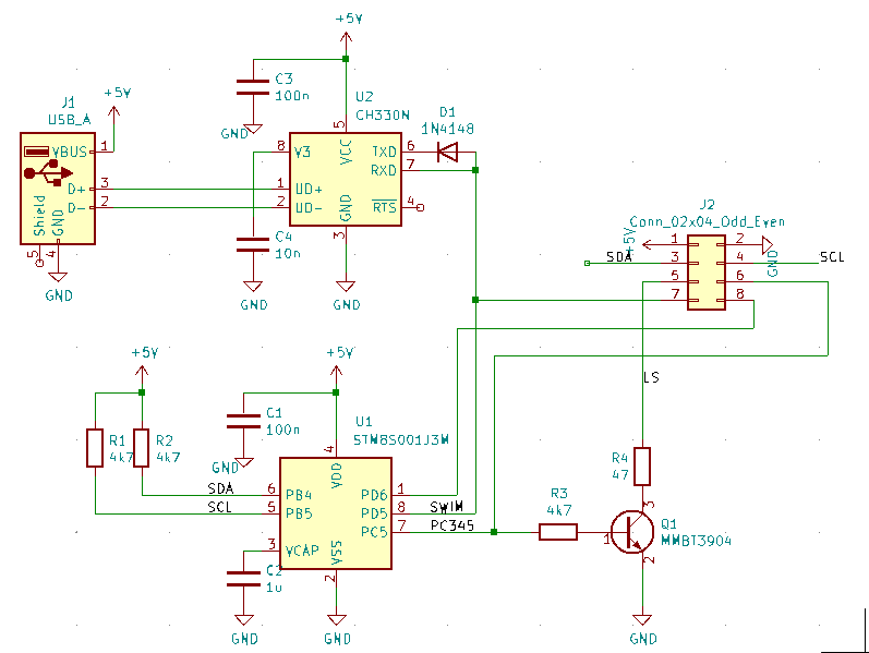
This is a design for an easy to use and easy to make key-chain sized STM8S001J3M3 dongle with CH330N USB-UART, e.g. for STM8 eForth (which turns it into an interactive development environment). It can also be for interfacing, e.g., 1Wire or I2C sensors, as an IR-code transmitter, or prototyping software for "Low density" STM8S µCs (which all have 8K Flash, 1K RAM and 128-640 bytes EEPROM). If you're an 8bit computing and retro-computing affectionado: the typical performance is like a "6502 @ >20MHz" and it's about as easy to program.

The STM8S001J3M3 UART works in "half-duplex" mode (PD5/UART_TX) with the CH330N USB-UART in wired-or configuration (D1). The internal pull-up of PD5 should be active (the STM8 eForth STM8S001J3 base image takes care of that). This configuration allows IAP (in application programming) in Forth and ICP (in circuit programming) through PD1/SWIM through pin8 of the µC.
All components, including the PCB and the SMD USB-A connector are easy to obtain (e.g. here for the USB connector - refer to the BOM is in the docs folder).

J2 provides the following signals:
| Pin | Label | Pin STM8S001 | GPIO | Features |
|---|---|---|---|---|
| 1 | 5V | 4 | VDD | 5V from USB or external supply |
| 2 | GND | 2 | VSS | GND |
| 3 | SDA | 5 | PB5 | I2C_SDA w/ 4k7 pull-up |
| - | 5 | PA3 | TIM2_CH3, [SPI_NSS], [UART1_TX] | |
| 4 | SCL | 6 | PB4 | I2C_SCL w/ 4k7 pull-up, [ADC_ETR] |
| 5 | LSS | PC3 | NPN "Low Side" switch w/ 47R, e.g. IR LED @ 100mA | |
| 6 | PC3 | 7 | PC3 | TIM1_CH3, [TLI], [TIM1_CH1N] same as LS NPN base |
| - | 7 | PC4 | TIM1_CH4, CLK_CCO, AIN2, [TIM1_CH3] | |
| - | 7 | PC5 | SPI_SCK, [TIM2_CH1] | |
| 7 | SWIM | 8 | PD1 | SWIM |
| - | 8 | PC6 | SPI_MOSI, [TIM1_CH1] | |
| - | 8 | PD3 | TIM2_CH2, TIM2_CH2, ADC_ETR | |
| - | 8 | PD5 | UART1_TX, AIN5 | |
| 8 | PD6 | 1 | PD6 | UART1_RX, AIN6 |
| - | 1 | PA1 | [OSC_IN] |
Note: the circuit relies on the USB port short-circuit protection!
Populating the PCB by hand is easy. I recommend starting with D1, then U1, U2, C1 and C2. On the front side populate Q1 and the passive components first, then J1 and finally J2.
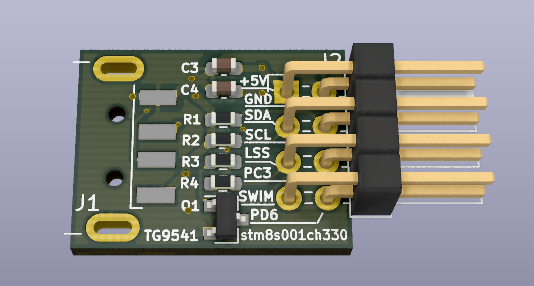
The following components are optional (e.g. if J2 isn't needed): R1, R2, R3, R4, Q1 and J2.
| Qty | Value | Footprint | References |
|---|---|---|---|
| 3 | 4k7 | Resistor_SMD:R_0603_1608Metric | R1, R2, R3 |
| 2 | 100n | Capacitor_SMD:C_0603_1608Metric | C1, C3 |
| 1 | 10n | Capacitor_SMD:C_0603_1608Metric | C4 |
| 1 | 1N4148 | Diode_SMD:D_MiniMELF | D1 |
| 1 | 1u | Capacitor_SMD:C_0603_1608Metric | C2 |
| 1 | 47 | Resistor_SMD:R_0603_1608Metric | R4 |
| 1 | CH330N | Package_SO:SOIC-8_3.9x4.9mm_P1.27mm | U2 |
| 1 | Conn_02x04_Odd_Even | Connector_PinHeader_2.54mm:PinHeader_2x04_P2.54mm_Horizontal | J2 |
| 1 | MMBT3904 | Package_TO_SOT_SMD:SOT-23 | Q1 |
| 1 | STM8S001J3M | Package_SO:SOIC-8_3.9x4.9mm_P1.27mm | U1 |
| 1 | USB_A | Connector_USB:USB_A_CNCTech_1001-011-01101_Horizontal | J1 |
TG9541/stm8s001rs485
A narrow KiCad made PCB with STM8S001J3, RS485 driver and DS1621S Thermometer, e.g., for STM8EF-MODBUS


windowsair/wireless-esp8266-dap
CMSIS-DAP compatible wireless debugger for ESP8266/ESP32/ESP32C3/ESP32S3. Optional 40MHz SPI acceleration, etc. 适配多种ESP芯片的无线调试器


szbeni/forcegauge
Traning for climbing. Load cell with HX711 and real time plotting,
It measures 18.3 × 14.2 mm and has 2 copper layers, 1.6 mm thick.
14 parts, built around the STM8S001J3M3, CH330N and MMBT3904. The full list of its parts is on this page, with links to each part's symbol and footprint where PCBKit's library has them.
From the TG9541/stm8s001ch330 repository on GitHub, at the commit this page was made from: the board is stm8s001ch330.kicad_pcb. PCBKit opens the board in the browser, with nothing to install.
Its repository publishes it under the CC0-1.0 licence: you may reuse it on that licence's terms (keep the author's notice, and for a copyleft licence share your changes alike).