2 layers80 × 50 mm
Main ctrl esp32 servo
Spectating101/hardware-splicer
Auditable hardware bring-up: donor → KiCad carrier + DRC + bench gates → PROJECT_PACKAGE. Seeking 3 design partners.
13 partsMIT
 Spectating101/hardware-splicer
Auditable hardware bring-up: donor → KiCad carrier + DRC + bench gates → PROJECT_PACKAGE. Seeking 3 design partners.
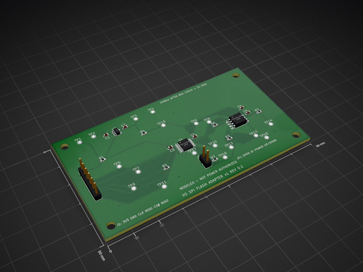
Spi flash adapter v1 is an open-source printed circuit board by Spectating101, from the Spectating101/hardware-splicer repository on GitHub, published under the MIT licence. It is a 2-layer board of 90 × 50 mm with 40 parts on 19 nets, routed with 155 tracks and 20 vias.
It is built around the W25Q128JWSIQ, RC0603FR-0710KL and RC0603JR-070RL, with the TSW-102-07-T-S and TSW-106-07-T-S among its other parts. Its parts include 7 resistors, 6 capacitors, 3 ICs and 1 connector. It belongs with the interfaces and adapters boards of this library.


This directory is the first complete Hardware Splicer reference design for the frozen 3.3 V-host to 1.8 V W25Q128JW case. It contains an editable KiCad 9 schematic, a routed two-layer PCB, an exact BOM, a machine-readable evidence/authority manifest, and scripts that regenerate, verify, and package the work without an external design contractor.
The current artifact is a bounded pre-fabrication result. It is internally consistent and reviewable, but it is not fabrication-authorized, power-on-authorized, or physically validated.
J1: 3.3 V host interface ordered as 3V3, GND, CLK, MOSI, CS#, MISO.U1: TXU0304PWR with three fixed A-to-B paths and one B-to-A path.U2: W25Q128JWSIQ in the SOIC-8 208-mil package.U3: TLV75518PDBVR fixed 1.8 V regulator.R1: removable host-power/current-measurement link, initially DNP.R4: removable DUT-domain isolation/current-measurement link, initially DNP.R2/R3: 10 kOhm defined-high bias for IO2/WP# and IO3/HOLD#.R5: 10 kOhm host-CS pull-up to HOST_3V3 upstream of R1. A powered host's
CS signal therefore cannot feed the isolated board supply through this resistor.R6: 10 kOhm DUT-CS pull-up to DUT_1V8, maintaining deselection while U1 is disabled.R7: 10 kOhm OE pull-down. JP1 is a normally open, two-pin enable header;
no shunt is fitted or supplied in the initial assembly variant.The initial proposed transaction is read-only command 0x9F at 5 MHz, SPI mode 0. Program, erase,
status-write, and reset commands are outside the first-use procedure.
Revision 0.2 corrects the original revision's automatic enable, absent CS bias, long ground-return tree, incomplete read timing calculation, and unbound design-rule checks. These are design corrections based on model review; human EE sign-off remains incomplete.
The selected topology is tied to frozen manufacturer-document identities in
design_manifest.json:
HardwareSplicer.kicad_sym contains project-local TXU0304PW and W25Q128JWS symbols.
U1 has the actual input and three-state output types, so ERC sees the fixed directions.
U2 points to the JW manufacturer datasheet and uses its SOIC-8 pinout. The selected IQ
suffix has QE fixed high: IO2/IO3 bias is not hardware write protection. The initial
read-only restriction is an operating procedure, not a hardware command filter.
Run:
python3 verify_design.pyThe verifier fails closed unless all of the following are zero:
verification.json binds those results to hashes of the canonical schematic, routed PCB,
BOM, design manifest, project rules, symbol library/table, and verification logic.
KiCad 9.0.2 produced the checked-in receipt. Structured native ERC/DRC JSON must match
the recognized schemas and stdout counts; missing arrays, unknown severities, exclusions,
unrecognized violation types, and mismatched counts fail closed.
KiCad's lib_footprint_mismatch is advisory only for a specifically identified footprint
whose installed-library and embedded pad stacks independently match: pin numbers, positions,
sizes, shapes, drill, layers, orientation, corner geometry, and mask/paste overrides.
Every other difference or violation is fatal. Non-pad graphics differences are recorded in
the receipt. This accommodates library-revision graphics drift without a blanket waiver.
The back ground fill must form one connected outline covering over 3000 mm2; both sides
must be filled, and each IC and bypass-capacitor ground pad must have a ground via within
2 mm. Non-ground routing on the back layer is rejected. These geometric checks do not prove impedance, return current distribution, or
signal integrity. The read-return budget now includes the outward clock translator:
100 - 19 - 6 - 15 = 60 ns, before interconnect, load, skew, and host setup terms.
Schematic generation requires kicad-sch-api==0.5.6 and KiCad 9 symbol libraries:
python3 -m venv /tmp/hs-kicad-sch
/tmp/hs-kicad-sch/bin/pip install kicad-sch-api==0.5.6
/tmp/hs-kicad-sch/bin/python generate_schematic.py
The PCB generator consumes KiCad's netlist exported from that schematic. This is deliberate: a geometrically clean board is rejected if its component identity, net names, or schematic paths do not have parity with the schematic.
Routing is pinned to Freerouting v2.4.1 and then independently accepted by KiCad. The
official freerouting-2.4.1-linux-x64.zip used here has SHA-256
3ad5a956ab474b12f331d24195feadac90e8344b8e013c6a4ab26e203ce51519.
python3 route_pcb.py --freerouting /path/to/freerouting-2.4.1-linux-x64/bin/freerouting
python3 verify_design.py
The router is an implementation tool, not an authority source. A routing run receives no credit unless the imported result passes KiCad DRC, connectivity, and schematic parity. Freerouting's zone/clearance diagnostics are printed separately. KiCad refills the ground zones after importing the session and is the acceptance check for the canonical result.
python3 build_package.py --output out/spi_flash_adapter_v1-review-package.zipThe package contains the canonical KiCad sources, design/BOM/verification records,
schematic and top-layer SVGs, copper/mask/paste Gerbers, separated plated/non-plated drill files, placement
CSV, and a per-file SHA-256 list. KiCad wall-clock fields and ZIP timestamps are normalized,
so repeated packaging of the same canonical inputs is byte-identical. These files remain
review inputs only; their
presence does not set fabrication_ready to true. The assembly BOM marks R1/R4 DNP and
the surface-mount placement export excludes them. J1/JP1 are through-hole parts, fitted
separately; JP1's header is fitted but its enable shunt is absent.
The following is a proposed bench procedure for independent review, not a power-on authorization. Record the exact host, instrument setup, current limits, and acceptance values before execution. Use a common ground first; keep the host supply and bench supply from being connected together through R1.
R1 and R4 DNP, JP1 open, and J1 disconnected. Verify the actual
flash marking/package and all component orientations.0x9F at 5 MHz and compare the observed ID with EF6018.Until that sequence is reviewed and completed, physical correctness remains UNPROVEN.
For execution by a PCBA functional-test service or remote laboratory, build the deterministic campaign projection:
python3 build_remote_fct_campaign.py \
  --output out/spi-flash-adapter-v1-remote-fct.zip
The outer archive contains the actual byte-bound fabrication, assembly, BOM, placement,
schematic and bounded host-test artifacts—not only metadata references—plus native KiCad
reports, the historical Astra source packet, an implementation-specific physical packet,
provider return template and PACKAGED_NOT_PHYSICAL Gauntlet state. Contact data and vendor
credentials are excluded. A successful build does not authorize fabrication or power.
| Qty | Value | Footprint | References |
|---|---|---|---|
| 5 | 10k | Resistor_SMD:R_0603_1608Metric | R2, R3, R5, R6, R7 |
| 4 | M3 | MountingHole:MountingHole_3.2mm_M3 | H1, H2, H3, H4 |
| 3 | 100nF 16V X7R | Capacitor_SMD:C_0603_1608Metric | C3, C4, C5 |
| 3 | GND | TestPoint:TestPoint_Pad_D1.5mm | TP4, TP17, TP18 |
| 2 | 0R | Resistor_SMD:R_0603_1608Metric | R1, R4 |
| 2 | 1uF 10V X7R | Capacitor_SMD:C_0603_1608Metric | C1, C6 |
| 1 | 1V8 | TestPoint:TestPoint_Pad_D1.5mm | TP3 |
| 1 | 3V3 | TestPoint:TestPoint_Pad_D1.5mm | TP2 |
| 1 | 4.7uF 6.3V X5R | Capacitor_SMD:C_0603_1608Metric | C2 |
| 1 | DUT_1V8 | TestPoint:TestPoint_Pad_D1.5mm | TP15 |
| 1 | DUT_CS_N | TestPoint:TestPoint_Pad_D1.5mm | TP10 |
| 1 | DUT_IO2_WP_N | TestPoint:TestPoint_Pad_D1.5mm | TP13 |
| 1 | DUT_IO3_HOLD_N | TestPoint:TestPoint_Pad_D1.5mm | TP14 |
| 1 | DUT_MISO | TestPoint:TestPoint_Pad_D1.5mm | TP12 |
| 1 | DUT_MOSI | TestPoint:TestPoint_Pad_D1.5mm | TP8 |
| 1 | DUT_SCLK | TestPoint:TestPoint_Pad_D1.5mm | TP6 |
| 1 | ENABLE_AFTER_RAIL_CHECK | Connector_PinHeader_2.54mm:PinHeader_1x02_P2.54mm_Vertical | JP1 |
| 1 | HOST_3V3 | TestPoint:TestPoint_Pad_D1.5mm | TP1 |
| 1 | HOST_CS_N | TestPoint:TestPoint_Pad_D1.5mm | TP9 |
| 1 | HOST_MISO | TestPoint:TestPoint_Pad_D1.5mm | TP11 |
| 1 | HOST_MOSI | TestPoint:TestPoint_Pad_D1.5mm | TP7 |
| 1 | HOST_SCLK | TestPoint:TestPoint_Pad_D1.5mm | TP5 |
| 1 | HOST_SPI_1x06 | Connector_PinHeader_2.54mm:PinHeader_1x06_P2.54mm_Vertical | J1 |
| 1 | TLV75518PDBVR | Package_TO_SOT_SMD:SOT-23-5 | U3 |
| 1 | TRANSLATOR_OE | TestPoint:TestPoint_Pad_D1.5mm | TP16 |
| 1 | TXU0304PWR | Package_SO:TSSOP-14_4.4x5mm_P0.65mm | U1 |
| 1 | W25Q128JWSIQ | Package_SO:SOIC-8_5.3x5.3mm_P1.27mm | U2 |
Spectating101/hardware-splicer
Auditable hardware bring-up: donor → KiCad carrier + DRC + bench gates → PROJECT_PACKAGE. Seeking 3 design partners.

Spectating101/hardware-splicer
Auditable hardware bring-up: donor → KiCad carrier + DRC + bench gates → PROJECT_PACKAGE. Seeking 3 design partners.

Spectating101/hardware-splicer
Auditable hardware bring-up: donor → KiCad carrier + DRC + bench gates → PROJECT_PACKAGE. Seeking 3 design partners.

aram-ap/daredevil
Computer Vision-Based Tactile Feedback for the Visually Impaired

holoindustry/AxxSolder_modded
Interested in purchasing an AxxSolder 3.2? On my website 5Dimensions you can purchase assembled and tested AxxSolder 3.2 boards with connectors and hardware.


rbrtwtrs/A2D-Test
Rev A ESP32-P4 Nano bench simulator/operator1.2. Companion: https://github.com/rovshop/herc-hotel-p4-firmware


ccc909/Whistler
Open-source 16-channel USB MEMS microphone array: KiCad PCB design, XMOS XU316 (xcore.ai) USB Audio Class 2 firmware with DFU, BOM and JLCPCB-ready production files. CERN-OHL-S.

Resident-X/brew-state
brew-state: bare-metal C state estimation and forward-horizon profiling for the Sunbeam EM7000. Built with Staircase.
It measures 90 × 50 mm and has 2 copper layers, 1.6 mm thick.
40 parts, built around the W25Q128JWSIQ, RC0603FR-0710KL, RC0603JR-070RL and TSW-102-07-T-S. The full list of its parts is on this page, with links to each part's symbol and footprint where PCBKit's library has them.
From the Spectating101/hardware-splicer repository on GitHub, at the commit this page was made from: the board is hardware/reference_designs/spi_flash_adapter_v1/spi_flash_adapter_v1.kicad_pcb and its schematic hardware/reference_designs/spi_flash_adapter_v1/spi_flash_adapter_v1.kicad_sch. PCBKit opens the board in the browser, with nothing to install.
Its repository publishes it under the MIT licence: you may reuse it on that licence's terms (keep the author's notice, and for a copyleft licence share your changes alike).