

2 layers75 × 55 mm
 SheinbergLab/dserv2
Data server system for data acquisition and control
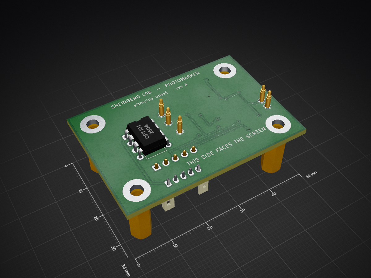
Photomarker is an open-source printed circuit board by SheinbergLab, from the SheinbergLab/dserv repository on GitHub, published under the MIT licence. It is a 2-layer board of 50 × 34 mm with 31 parts on 12 nets, routed with 92 tracks and 13 vias.
It is built around the OPT101P and LM393. Its parts include 14 resistors, 3 capacitors, 2 ICs, 2 connectors and 1 diode.
Sheinberg Lab — rev A
A per-rig photodiode board that timestamps stimulus light onset two ways at once: an analog waveform into an MCP3204 channel, and a comparator edge into a dserv DI pin (IRQ-latched with a box-clock stamp, so it beats the ~100 µs ADC scan quantization).
Wire both. The digital edge is your routine per-trial timestamp; the analog trace is how you verify the edge means what you think, because a fixed voltage threshold lands at a different fraction of the transition for black→white than for a gray-to-gray change.
REV in gen_photomarker.pyThe board is generated, not hand-drawn. Edit gen_photomarker.py (placement
table + routing table near the top) and re-run:
/Applications/KiCad/KiCad.app/Contents/Frameworks/Python.framework/Versions/3.9/bin/python3 gen_photomarker.pyTwo API gotchas baked into the script, both found the hard way:
board.Add(fp) must precede fp.Flip() (flipping an unparented footprint
segfaults), and the flip is an X-mirror — verified empirically rather than
assumed.
Top faces the screen. Only the OPT101 is up there, standing 4.19 mm proud so nothing shadows it.
Bottom carries all SMD — single-sided assembly at JLCPCB, and the board itself blocks the bring-up LED's light from reaching the photodiode.
Upload fab/photomarker-gerbers.zip. For assembly add
fab/photomarker-cpl.csv and fab/photomarker-bom.csv.
The BOM's LCSC Part # column is deliberately empty. Fill it from JLCPCB's
parts search — do not trust a guessed C-number, it orders the wrong part.
JLCPCB places 10 parts: U2, R1–R5, R11, C1–C3. Everything else is DNP or hand-soldered. At that count, hand-soldering a SOIC-8 and nine 0805s may well cost less than the assembly setup fee — worth pricing both ways.
| Ref | Part | Note |
|---|---|---|
| U1 | OPT101, DIP-8 | Mount from the top. Strap pin 4 (1M) to pin 5 (OUT) is on the PCB already. |
| J1 | JST-PH B5B-PH-K, 5-pin vertical | On the bottom, so the cable exits away from the screen. |
OPT101 handling: TI warns the clear plastic is moisture-sensitive and that rapid heating can stress the wire bonds. If the parts have sat in humidity, bake at 85 °C for 24 h first. Solder gently either way.
Pin 1 is leftmost. Silkscreen reads 3V3 GND AO DIb DIa.
| Pin | Net | To the extio box |
|---|---|---|
| 1 | +3V3 | 3V3 |
| 2 | GND | GND |
| 3 | AOUT | MCP3204 CH2 (CH0/CH1 are the joystick) |
| 4 | DI-B | free GPIO — optional second threshold |
| 5 | DI-A | free GPIO — main onset edge |
Free GPIOs per wiznet-io/PINMAP.md: 9–14, 26, 27.
Output goes LOW on light onset (signal on IN−), so configure that DI for the falling edge.
On the ain group carrying CH2: set deadband 0 and average 1. Both smear
the edge, which is the one thing you are trying to measure.
Threshold network on 3.3 V, R1 = 39 k, R2 = 10 k, R3 = 270 k:
Because the signal is on IN−, the hysteresis lands entirely on the release side — it costs nothing on the onset edge, so be generous with it.
Aim the threshold at ~50 % of your lit-state level, not 20 %. Mid-transition is steepest, so timing there is least sensitive to stimulus amplitude drift. The resulting latency to true onset is a constant: measure it once off the analog trace and subtract.
Retune by swapping R1 alone:
| R1 | Onset | Hysteresis |
|---|---|---|
| 68 k | 0.513 V | 103 mV |
| 39 k | 0.749 V | 94 mV |
| 27 k | 0.955 V | 87 mV |
| 18 k | 1.228 V | 77 mV |
| 12 k | 1.536 V | 65 mV |
C3 must be C0G/NP0, not X7R — X7R drifts with temperature and DC bias, which would move the filter corner and turn your calibrated constant lag into a drifting one.
The footprint is SOIC-8 and the two parts are pin-identical (1=OUT_A, 2=IN_A−, 3=IN_A+, 4=GND, 5=IN_B+, 6=IN_B−, 7=OUT_B, 8=VCC).
The LM393's common-mode ceiling (V+ − 1.5 V ≈ 1.8 V at 3.3 V) is not a problem at this operating point, since the threshold is 0.749 V and the lit level is ~1.5 V by design. There is no 5 V anywhere on the board, so nothing can put 5 V on a GPIO.
| Ref | Purpose |
|---|---|
| R6 | External gain resistor across the OPT101 feedback — fit this if you saturate, which is likely at 0.45 V/µW |
| R8 | Parallel with R1 for fine threshold trim |
| R7, R14 | Pull-ups, LM393 only |
| R9, D1 | Bring-up LED on the comparator output. D1 pin 1 = cathode (KiCad convention), so the anode faces R9 / +3V3 and the LED lights when the output goes low on light onset |
| R12, R13, R15 | Comparator B's second threshold → DI-B. Populate to time the 25 %→75 % crossing and measure the panel's transition slope in hardware, per trial |
| J2 | 0.1" alternative to J1, same pinout |
R11 (10 k) is fitted, not DNP. With the B network unpopulated it pulls comparator B's IN+ to 3.3 V — definitively above IN−'s ~2.0 V ceiling — so that comparator parks HIGH instead of oscillating on a floating input, and DI-B carries a defined level. Re-value it into a real divider with R12 when you actually want the second threshold.
Test points: TP1 OPT_OUT, TP2 FILT, TP3 THRESH, TP4 CMP_OUT, TP5 GND.
photomarker.kicad_sch + schematic.pdf. ERC clean (0 violations), and verified
against the board by check_netlist.py — which compares nets, refs, values,
footprints and DNP flags, not just connectivity. All 12 nets match exactly; the
only schematic-side extras are the OPT101's two NC pins, deliberately unconnected
on both sides.
Run it before ordering and after any regeneration (exit status 0 = agreement):
/Applications/KiCad/KiCad.app/Contents/Frameworks/Python.framework/Versions/3.9/bin/python3 check_netlist.pyIt is generated by gen_schematic.py, which reads the netlist out of
photomarker.kicad_pcb — so the schematic cannot silently drift from the
board. Regenerate after any board change:
/Applications/KiCad/KiCad.app/Contents/Frameworks/Python.framework/Versions/3.9/bin/python3 gen_schematic.pyConnectivity is by net label rather than drawn wire, with components grouped by function. That is a deliberate choice for a generated schematic: label connectivity is verifiable by ERC and by netlist diff, where hand-computed wire geometry can look connected while being 0.01 mm short.
KiCad ships neither part, so photomarker.kicad_sym defines both:
output pins instead of open_collector.sym-lib-table maps photomarker: to the local library, so the project opens
standalone.
Drawing it found a real bug in the board: KiCad's Device:LED has pin 1 =
cathode, but D1 pin 1 had been wired to the resistor from +3V3 — the indicator
LED was reverse-biased. Fixed by swapping the net assignment and flipping D1.
Worth remembering if you add any other polarised part.
| Qty | Value | Footprint | References |
|---|---|---|---|
| 5 | DNP | R_0805_2012Metric | R6, R8, R12, R13, R15 |
| 4 | M3 | MountingHole_3.2mm_M3_Pad | H1, H2, H3, H4 |
| 3 | 10k | R_0805_2012Metric | R2, R4, R11 |
| 2 | 100n | C_0805_2012Metric | C1, C2 |
| 2 | 2k2 | R_0805_2012Metric | R7, R14 |
| 1 | 100R | R_0805_2012Metric | R5 |
| 1 | 270k | R_0805_2012Metric | R3 |
| 1 | 39k | R_0805_2012Metric | R1 |
| 1 | 3n3 C0G | C_0805_2012Metric | C3 |
| 1 | CMP_OUT | TestPoint_THTPad_D1.5mm_Drill0.7mm | TP4 |
| 1 | DNP 1k | R_0805_2012Metric | R9 |
| 1 | DNP 1x05 | PinHeader_1x05_P2.54mm_Vertical | J2 |
| 1 | DNP LED | LED_0805_2012Metric | D1 |
| 1 | FILT | TestPoint_THTPad_D1.5mm_Drill0.7mm | TP2 |
| 1 | GND | TestPoint_THTPad_D1.5mm_Drill0.7mm | TP5 |
| 1 | JST-PH 5 | JST_PH_B5B-PH-K_1x05_P2.00mm_Vertical | J1 |
| 1 | LM393 | SOIC-8_3.9x4.9mm_P1.27mm | U2 |
| 1 | OPT101 | DIP-8_W7.62mm | U1 |
| 1 | OPT_OUT | TestPoint_THTPad_D1.5mm_Drill0.7mm | TP1 |
| 1 | THRESH | TestPoint_THTPad_D1.5mm_Drill0.7mm | TP3 |

open3doled/open-3d-oled
If running windows 11 or 10 with DPI scaling be sure to disable it as follows. 1) Right click properties on 3dplayer.exe in the 3DPlayer folder 2) Click on "Compatability" tab then click on the button at the bottom…

nguyenhuy0426/PPG_simulator
The PPG Signal Simulator is a portable device that generates synthetic PPG (photoplethysmography) waveforms with physiologically accurate morphology.

AlessandroLovo/T-junction
Analysis of data from a Microfluidic T-juction. Course of Advanced Physics Laboratory @ Università degli studi di Padova

jayis1/hardware-design-lab
Full-cycle hardware device designs — each device in its own subfolder with architecture, schematics, PCB layout, and software stack


schlae/snark-barker-mca
A Sound Blaster compatible sound card for Micro Channel bus computers
It measures 50 × 34 mm and has 2 copper layers, 1.6 mm thick.
31 parts, built around the OPT101P and LM393. The full list of its parts is on this page, with links to each part's symbol and footprint where PCBKit's library has them.
From the SheinbergLab/dserv repository on GitHub, at the commit this page was made from: the board is hardware/photomarker/photomarker.kicad_pcb and its schematic hardware/photomarker-tht/photomarker-tht.kicad_sch. PCBKit opens the board in the browser, with nothing to install.
Its repository publishes it under the MIT licence: you may reuse it on that licence's terms (keep the author's notice, and for a copyleft licence share your changes alike).