6 layers83.5 × 99.4 mm

 Senyeah/12v-to-usb-c-data-splitter
Car 12 V to USB-C 5 V 3 A (15 W) charger that passes the stereo's USB data through to the phone. KiCad 10, JLCPCB-ready.
Swift usbc-3a is an open-source printed circuit board by Senyeah, from the Senyeah/12v-to-usb-c-data-splitter repository on GitHub, published under the CERN-OHL-S-2.0 licence. It is a 4-layer board of 52 × 40 mm with 48 parts on 30 nets, routed with 230 tracks and 73 vias.
It is built around the MPQ4228GRE-C-AEC1-Z, PESD5V0U1UA and SMBJ33CA, with the SS510 among its other parts. Its parts include 21 capacitors, 11 resistors, 6 diodes, 4 inductors and 3 connectors. It belongs with the power boards of this library.


A car board that turns 12 V into 5 V at 3 A (15 W) on a USB-C socket for the phone, and passes the factory stereo's USB data through to the same phone. I made it for a car stereo that talks to the phone over the old iPod USB protocol, and an iPhone 15 Pro. The board does not use USB PD, so the iPhone keeps its USB data link to the stereo while it charges.
v1 is built, and it works great.
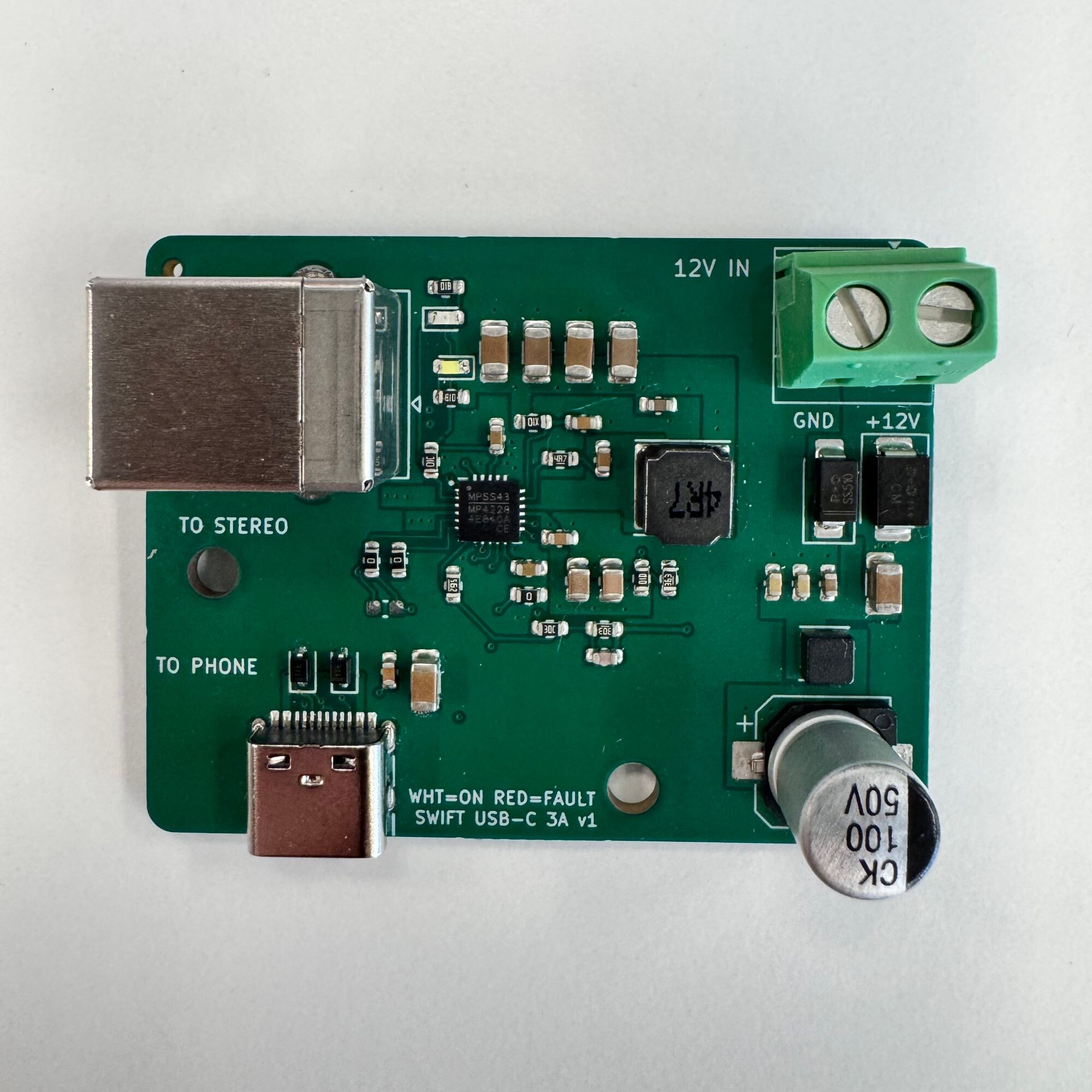
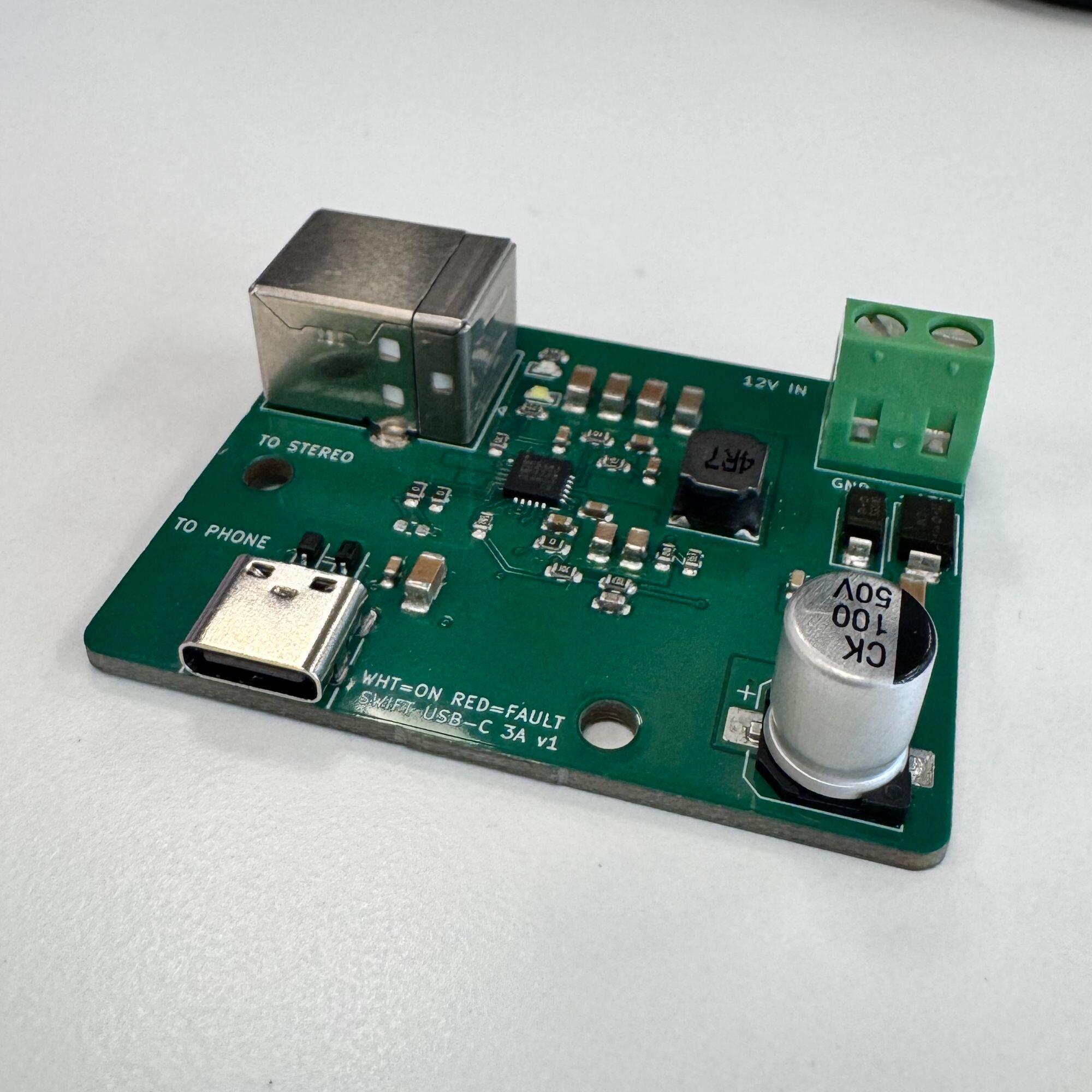
fab/: the Gerber zip to upload, the same files unzipped in fab/gerber/, JLCPCB BOM and CPL files in
fab/assembly/, and schematic, assembly and layer PDFs in fab/docs/.docs/: 3D renders, an A5 schematic PDF and the photos above.lib/.scripts/: the KiCad Python scripts that built the schematic fields, the routing and the fab pack.sim/: ngspice simulation of the input chain and hand calculations, with results.JLCPCB was the cheapest fab I found. Upload the Gerber zip from fab/.
fab/assembly/*-bom-jlc.csv. CPL: fab/assembly/*-cpl-jlc.csv. In the BOM step, tick the "L3,L4,R9" (0R)
line: JLC leaves it unselected.JLCPCB quote on 07/10/2026 for 5 boards with 2 assembled:
| Line | US$ |
|---|---|
| PCB | 8.00 (2.00 through the JLCONE desktop app) |
| Setup 8.24 + stencil 1.55 | 9.79 |
| Components, 30 lines | 14.27 |
| Extended components fee (U1, J3, C1, L1, L2, C2/C3, D3/D4) | 21.63 |
| SMT assembly, placement check, nitrogen reflow | 1.88 |
| Shipping, Global Standard Direct Line | 7.24 |
| Automatic cart coupon | −10.00 |
| Total before GST | ≈ 52.81 (≈ NZ$90); ≈ US$61 / NZ$103 with 15 % GST |
The GST line and new-user coupons only show at checkout, after you enter the shipping address.
J1 (screw terminal) and J2 (USB-B) are through-hole. If you do not want to solder anything, upload
fab/assembly/*-with-tht-bom-jlc.csv and fab/assembly/*-with-tht-cpl-jlc.csv instead. JLC then hand-solders both
parts in Economic PCBA for US$5.61 more (US$61.18 instead of US$55.57 on 07/10/2026; hand-soldered parts have no
extended fee). Otherwise buy C7509570 and C19944605 and solder the 10 joints yourself.
The CPL files shift J1, J2 and J3 so that JLC's (EasyEDA) footprint origins land on the KiCad footprints (CPL_FIX in
scripts/jlc_files.py). Without the shift, JLC's preview puts J3 1.42 mm towards the board edge.
On 07/10/2026 PCBWay, Seeed, ALLPCB, NextPCB and Elecrow were all more expensive for 2 assembled boards. NextPCB's "Rev 0" free assembly offer could be cheaper, but it needs a live quote and its parts do not come from LCSC.
| Item | Source | NZ$ |
|---|---|---|
| Panel-mount USB-C male-to-female extension, USB 3.1 type (passes CC) | AliExpress 1005010641105986 | ≈ 6.30 |
| Short USB-A male to USB-B male cable | AliExpress 32700175631 or a spare printer cable | 0–5.60 |
| Micro2 add-a-circuit fuse tap and a 5 A Micro2 fuse | AliExpress 1005006019784140 or a car parts shop | ≈ 0.50–8 |
| 0.75–1 mm² wire, ring terminal for ground | on hand |
Wiring: console USB-A socket → USB-A to USB-B cable → J2. J3 → panel-mount USB-C extension → phone. Fuse tap on an ACC fuse → 5 A fuse → J1 "+12V". J1 "GND" → body ground near the stereo. The stereo's 5 V does not connect to anything on the board.
VBUS on J3 stays at 0 V until a sink attaches. That is correct: the white LED shows VOUT, not VBUS.
lib/ is drawn from the datasheet land pattern. Compare it with the JLC footprint preview
before you pay.MPS publishes no SPICE model for the MPQ4228 (SIMPLIS only), so the converter itself is not simulated.
sim/input_sim.py (ngspice) models the input chain with the chip as a 17.7 W constant-power load, through ISO
7637-2 and ISO 16750-2 pulses at both SMBJ33CA tolerance ends. Results are in sim/results.md. Everything passes
except the unsuppressed 87 V load dump (about 230 J into the TVS), which no small TVS survives. The board relies on
the car's alternator load-dump suppression, and a shorted TVS blows the 5 A fuse. Pulse 1 put 60.6 V across the
first-choice SS56 (60 V), so D2 is now an SS510 (100 V, 75.9 V seen). The input filter is stable, with at least 9 dB
margin at 6 V input.sim/calcs.py: output voltage 4.85–5.22 V at no load and at most 5.45 V at 3 A worst case; L1 peak at most 5.31 A
(Isat 5.5 A); U1 Tj ≈ 100–122 °C and D2 Tj ≈ 118 °C at 60–70 °C ambient. Results are in sim/calcs.md.Run the scripts with KiCad's Python (/Applications/KiCad/KiCad.app/Contents/Frameworks/Python.framework/Versions/3.9/bin/python3
on macOS). They assume KiCad 10 in /Applications.
scripts/make_lib.py (symbol and footprint), then add_fields.py and cost_parts.py (JLC basic part swaps) on the
schematic.scripts/rename_nets.py, then sync_parity.py (board from the schematic netlist).scripts/copper.py <board> --routing, then route.py <board> <workdir> (Freerouting, expected at
~/.kicad-mcp/freerouting.jar), then copper.py <board>.scripts/silk.py, then scripts/fab.sh to write fab/.uv run sim/input_sim.py and python3 sim/calcs.py for the checks.CERN Open Hardware Licence Version 2, Strongly Reciprocal (CERN-OHL-S-2.0). See LICENSE. Source: https://github.com/Senyeah/12v-to-usb-c-data-splitter
| Qty | Value | Footprint | References |
|---|---|---|---|
| 4 | 22uF 25V | Capacitor_SMD:C_1206_3216Metric | C21, C22, C23, C24 |
| 2 | 0R | Inductor_SMD:L_0603_1608Metric | L3, L4 |
| 2 | 100nF 50V | Capacitor_SMD:C_0603_1608Metric | C4, C13 |
| 2 | 10uF 50V | Capacitor_SMD:C_1206_3216Metric | C14, C27 |
| 2 | 1k | Resistor_SMD:R_0603_1608Metric | R10, R11 |
| 2 | 220nF | Capacitor_SMD:C_0603_1608Metric | C7, C25 |
| 2 | 22nF 50V | Capacitor_SMD:C_0603_1608Metric | C11, C12 |
| 2 | 4.7uF 50V | Capacitor_SMD:C_0805_2012Metric | C2, C3 |
| 2 | M3 | MountingHole:MountingHole_3.2mm_M3 | H1, H2 |
| 2 | PESD5V0U1UA | Diode_SMD:D_SOD-323 | D3, D4 |
| 1 | 0R | Resistor_SMD:R_0603_1608Metric | R9 |
| 1 | 100k | Resistor_SMD:R_0603_1608Metric | R1 |
| 1 | 100nF | Capacitor_SMD:C_0603_1608Metric | C20 |
| 1 | 100uF 50V | Capacitor_SMD:CP_Elec_8x10.5 | C1 |
| 1 | 10R | Resistor_SMD:R_0603_1608Metric | R5 |
| 1 | 10k | Resistor_SMD:R_0603_1608Metric | R3 |
| 1 | 12V IN | TerminalBlock_Phoenix:TerminalBlock_Phoenix_MKDS-1,5-2-5.08_1x02_P5.08mm_Horizontal | J1 |
| 1 | 1uF | Capacitor_SMD:C_0603_1608Metric | C5 |
| 1 | 2.2nF | Capacitor_SMD:C_0603_1608Metric | C28 |
| 1 | 2.2uH 4.7A | Inductor_SMD:L_Changjiang_FTC303020D | L2 |
| 1 | 20k | Resistor_SMD:R_0603_1608Metric | R6 |
| 1 | 3.3pF | Capacitor_SMD:C_0603_1608Metric | C29 |
| 1 | 30k 1% | Resistor_SMD:R_0603_1608Metric | R7 |
| 1 | 36k 1% | Resistor_SMD:R_0603_1608Metric | R2 |
| 1 | 4.7R | Resistor_SMD:R_0603_1608Metric | R4 |
| 1 | 4.7uF | Capacitor_SMD:C_0603_1608Metric | C6 |
| 1 | 4.7uH 3.6A | Inductor_SMD:L_APV_ANR6045 | L1 |
| 1 | 47pF C0G | Capacitor_SMD:C_0603_1608Metric | C26 |
| 1 | 5.6k 1% | Resistor_SMD:R_0603_1608Metric | R8 |
| 1 | FAULT red | LED_SMD:LED_0603_1608Metric | D6 |
| 1 | MPQ4228GRE-C-AEC1 | swift:MPS_QFN-22_4x4mm_P0.5mm | U1 |
| 1 | SMBJ33CA | Diode_SMD:D_SMB | D1 |
| 1 | SS510 | Diode_SMD:D_SMA | D2 |
| 1 | USB-B from stereo | Connector_USB:USB_B_OST_USB-B1HSxx_Horizontal | J2 |
| 1 | USB-C to phone | Connector_USB:USB_C_Receptacle_HRO_TYPE-C-31-M-12 | J3 |
| 1 | White LED | LED_SMD:LED_0603_1608Metric | D5 |

mx-yah/amp600w
A high-performance high-power class-D amplifier that enables true premium sound quality with high-efficiency class-D technology

ArthorH/ModuCard-Backplane-Sixth-Sense
Sixth sense for debugging 6 modules


Anderman/Renovent
Display is een liteon De 8 segementen worden in volgorde aan gestuurd met een freq van 500uS Welke segmenten verlicht worden gaat met digit 1 - 4

efebasol/StepperMotorController
Rev A — single-motor bench prototype power board. Feeds the driver board (48 V), the stepper motor brake (24 V) and the logic (5 V / 3V3).

Franzelfx/vertical-wind-turbine
Design study: a 3D-printed vertical-axis wind turbine on a timber post, charging a 3S Li-ion pack. Parts, circuit and figures generated by scripts with FreeCAD, KiCad and Blender. Nothing built yet.
It measures 52 × 40 mm and has 4 copper layers, 1.6 mm thick.
48 parts, built around the MPQ4228GRE-C-AEC1-Z, PESD5V0U1UA, SMBJ33CA and SS510. The full list of its parts is on this page, with links to each part's symbol and footprint where PCBKit's library has them.
From the Senyeah/12v-to-usb-c-data-splitter repository on GitHub, at the commit this page was made from: the board is swift-usbc-3a.kicad_pcb and its schematic swift-usbc-3a.kicad_sch. PCBKit opens the board in the browser, with nothing to install.
Its repository publishes it under the CERN-OHL-S-2.0 licence: you may reuse it on that licence's terms (keep the author's notice, and for a copyleft licence share your changes alike).