


2 layers38 × 26 mm
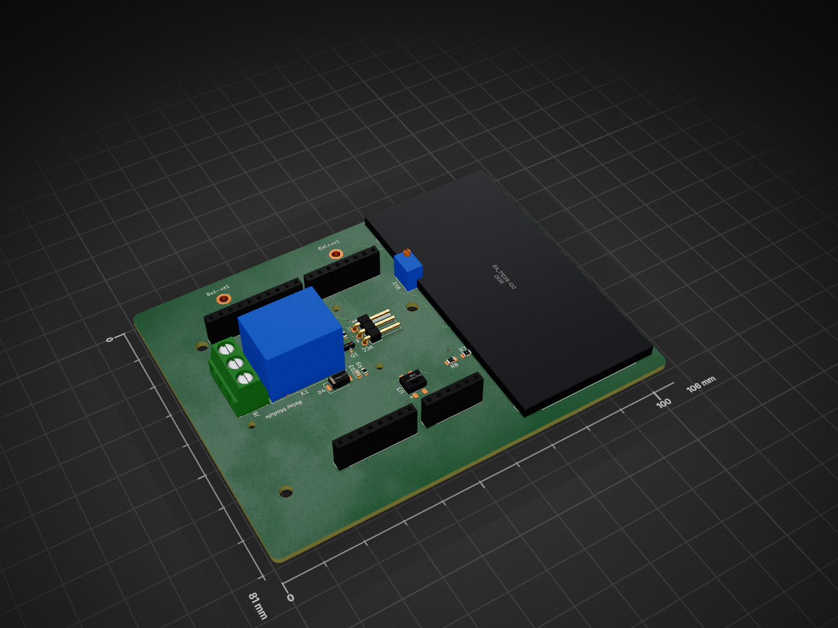
Created a load control system in which load connected to relay module is turned ON or OFF by entering a password using IR based remote. Built on arduino UNO R3 clone using CH340 chip.
Load Ctrl is an open-source printed circuit board by Nayan9ine, from the Nayan9ine/Load-Control-Using-Relay-Module-and-IR-Remote repository on GitHub. It is a 2-layer board of 106 × 81 mm with 25 parts on 40 nets, routed with 115 tracks and 3 vias.
It is built around the MMBT2222A and MRA4003T3G-MS. Its parts include 6 connectors, 5 resistors, 2 ICs, 2 diodes and 1 transistor. It belongs with the home automation and IoT and lEDs and displays boards of this library.
MADE ARDUINO SHIELD FOR LOAD CONTROL which has relay module IR receiver and LCD display embedded on it with a pot to control brightness.
->Learnt how to adjust arduino shield boundary layer to fit in components.
->How to use VIAS,Net Labels, Power FLags
->power GND symbols act as global labels so symbols with same name so get connected electrically.
->re matching pin reference numbers to their footprints
->Arduino sheild template was used, the entire boundary was fixed in one place.Was unable to expand the area to put my components in. Learnt about the "locked" feature and disabled it by using Appearance tab and Selection Filter.
->used fillet lines to round up sharp wire edges.
->to draw board outline: appearance->layers->Edge.Cuts -> choose drawing line or shape etc.
->changing sda/scl pins from digital to analog side in order for better routing
->using analog pin as digital for IR receiver for better routing
-> can keep signal traces (i2c scl sda) thin but keep them away from high freq signals (buck converter)
or relay module as they create heavy EMI. Never run them parallel to relay lines, cross only at 90 degrees to relay lines)
->signal lines: 0.2mm Power lines:0.4mm GND lines: 0.6mm
Appropriate Components Found:
-> RELAY MODULE DESIGN EXTRACTED from: (https://github.com/ampnics/Relay-Module-HW-Design) when copy-pasted from original schematic the resulting pcb desin was jumbled up so directly copy-pasted PCB design and chenaged the reference name to match the schematic so duplicate relay components won't be created again.
->The LCD I2C component I was able to find (EA T123X-I2C) was different than what was used in the project. It needed 2 4.7k Ohm pull up resistors for SDA,SCL. Has 2 additional pins for adjusting display contrast (Vo and Vlcd). The contrast was controlled by a potentiometer with Vlcd connected to gnd and 3rd pin of pot. 2nd pin to Vo and 1st to Vdd (5v).
->Added 2 pwr flags on Vo and Vdd as kicad ERC was throwing "input power pins not connected to source" error.
->made several connections using NET LABELS to avoid messy wiring.
->added no connect flags on pins not being used.
-> Mounting holes added to show LCD external 5V supply and AC load connection to relay thorugh a LAMP symbol.
->Since GND pins in arduino shield are assumed to be internally connected, KiCad ERC throws "No connection" error and DRC shows unecessary ratnets. So I had to change the name of various GND symbols and some labelled as No Connect.
->For smd resistors only traces in front can get connected so used vias to turn back trace into front then connect to smd.
| Qty | Value | Footprint | References |
|---|---|---|---|
| 4 | MountingHole_3.2mm | Arduino_MountingHole:MountingHole_3.2mm | MH1, MH2, MH3, MH4 |
| 2 | 10K | Resistor_SMD:R_0603_1608Metric | R9, R10 |
| 2 | 4.7K | Resistor_SMD:R_0805_2012Metric_Pad1.20x1.40mm_HandSolder | R7, R8 |
| 2 | MountingHole_Pad | MountingHole:MountingHole_2.2mm_M2_DIN965_Pad | Bat-ve1, Bat+ve1 |
| 1 | 1K | Resistor_SMD:R_0603_1608Metric | R4 |
| 1 | Analog | Connector_PinSocket_2.54mm:PinSocket_1x06_P2.54mm_Vertical | J3 |
| 1 | Conn_01x03_Pin | Connector_PinHeader_2.54mm:PinHeader_1x03_P2.54mm_Horizontal | J7 |
| 1 | Digital/PWM | Connector_PinSocket_2.54mm:PinSocket_1x08_P2.54mm_Vertical | J4 |
| 1 | Digital/PWM | Connector_PinSocket_2.54mm:PinSocket_1x10_P2.54mm_Vertical | J2 |
| 1 | EA_T123X-I2C | Display:NHD-C0220BiZ-FSRGB | U4 |
| 1 | IRM-H6xxT | OptoDevice:Everlight_IRM-H6xxT | U3 |
| 1 | LED | LED_SMD:LED_0603_1608Metric | D3 |
| 1 | MMBT2222A | Package_TO_SOT_SMD:SOT-23 | Q1 |
| 1 | MRA4003T3G | Diode_SMD:D_SMA | D4 |
| 1 | Potentiometer | Potentiometer_THT:Potentiometer_Bourns_3266Y_Vertical | RV2 |
| 1 | Power | Connector_PinSocket_2.54mm:PinSocket_1x08_P2.54mm_Vertical | J1 |
| 1 | SANYOU_SRD_Form_C | Relay_THT:Relay_SPDT_SANYOU_SRD_Series_Form_C | K1 |
| 1 | Screw_Terminal_01x03 | TerminalBlock:TerminalBlock_bornier-3_P5.08mm | J8 |
The 24 most common of 25 parts.

X-zeed/UTAC-PCB
4-channel smart relay control board with ESP32-C3 SuperMini - KiCad PCB Design v0.2.0


shetevaibhav014/5V-Single_Channel_Relay-Module
An open-source, production-ready 2-layer PCB design for a 5V Single-Channel Relay Module featuring safety-first routing.

dhivyaadevi-K/PCB-Design-Learning-Series
A structured collection of PCB design projects created using KiCad 9, documenting my learning journey from basic electronic circuits to advanced PCB layouts.

sandgum/Triangulate-ES_01-Watch
A 5mm thick smartwatch which uses an E-ink display and two OLEDs to display information while consuming very little power

It measures 106 × 81 mm and has 2 copper layers, 1.6 mm thick.
25 parts, built around the MMBT2222A and MRA4003T3G-MS. The full list of its parts is on this page, with links to each part's symbol and footprint where PCBKit's library has them.
From the Nayan9ine/Load-Control-Using-Relay-Module-and-IR-Remote repository on GitHub, at the commit this page was made from: the board is KiCad 9.0 Details/Load Ctrl.kicad_pcb and its schematic KiCad 9.0 Details/Load Ctrl.kicad_sch. PCBKit opens the board in the browser, with nothing to install.
Its repository states no licence, so its author keeps all rights: ask Nayan9ine before reusing the design.