
4 layers78 × 86 mm
SJ-201-R10
MycroftAI/hardware-mycroft-mark-II
Mycroft's Mark II Rpi mechanical, electrical and industrial designs
185 parts113

Mycroft's Mark II Rpi mechanical, electrical and industrial designs
SJ-201-R6 is an open-source printed circuit board by MycroftAI, from the MycroftAI/hardware-mycroft-mark-II repository on GitHub. It is a 4-layer board of 67 × 98 mm with 235 parts on 172 nets, routed with 2,927 tracks and 573 vias.
It is built around the ATTINY1614-SSN, SPK0641HT4H-1 and AMS1117-3.3, with the WS2812B, 330UF 25V 8*12 and AO3401A among its other parts. Its parts include 69 capacitors, 64 resistors, 16 diodes, 8 ICs and 8 connectors. It belongs with the AVR (ATmega, ATtiny) boards of this library.


This board interfaces directly to the Raspberry Pi 4 via the 40-pin GPIO adding a high-quality speaker and microphone array, as well as LEDs and hardware inputs for non-voice interaction and feedback.
The part number SJ201 is derived from Mike’s “Simon Jester” alias in “The Moon is a Harsh Mistress”.
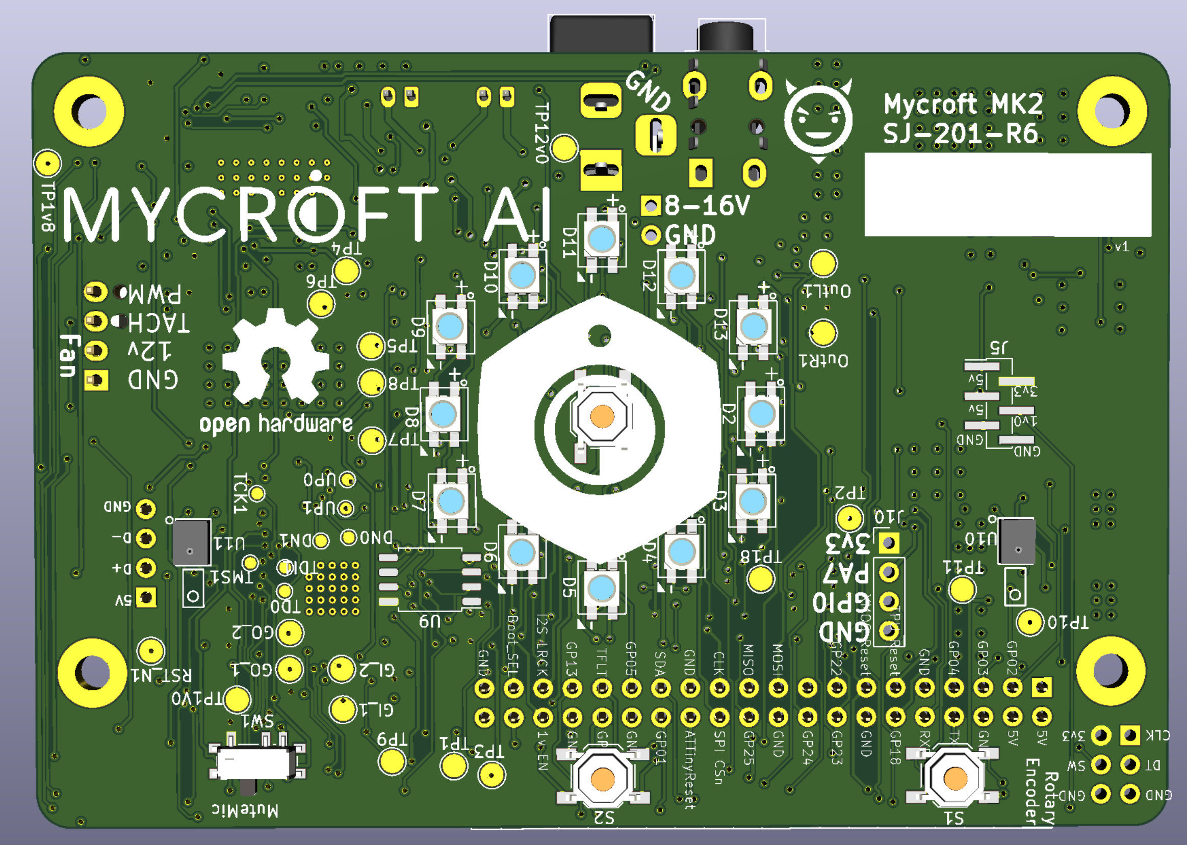
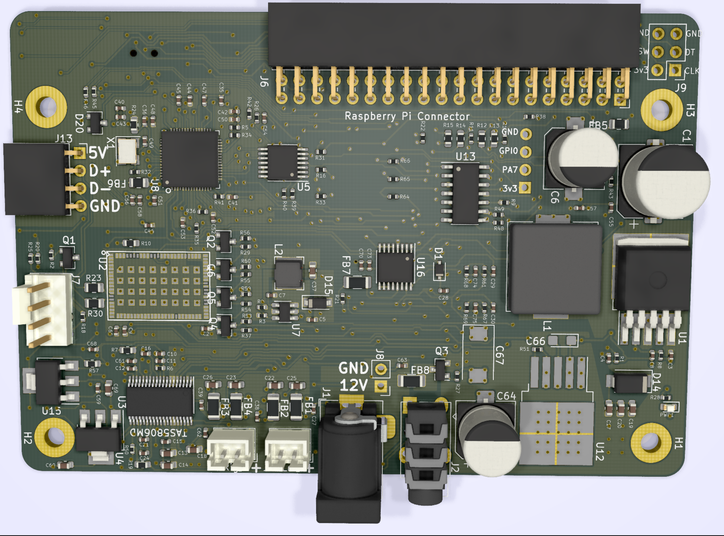
This Datasheet will contain all the relevant information for the manufacturing of the SJ201 including information about PCB design, PCB manufacturing process.
The SJ201 is connected to a Raspberry Pi4 via the header.
12V is supplied to the SJ201 via the barrel jack.
The SJ201 creates 5V using a 3A buck converter, which powers the Raspberry Pi.
The SJ201 creates 3.3V using a linear regulator, which powers the on-board devices.
4.4ohm, 5W speakers are connected to the JST connectors. [Note, in the current implementation the amplifier is capable of supplying 13W to each speaker, so volume must be limited in software to avoid damage.]
The J5 header serves as a test point for the 3.3V, 5V and 12V supplies.
The J5 header can also be used to bypass the on-board buck converter and/or linear regulator.
The buck converter does not need to be turned off - it can tolerate an external supply. To completely disable it, lift the appropriate pin.
The 1.0V supply can be tested using Test Point TP1_0V1 near the XMOS IC.
The SJ201 is powered by an external 12V 3A DC supply (wall wart) via a barrel connector. The SJ201 has 4 voltage domains:
VDD 12V externally supplied power
PVDD 12V Analog Audio Power
5V 5V derived from VDD
3V 3.3V derived from 5V
1V 1.0V derived from 5V for the XMOS core
All power domains share a common ground.
Filterless modulation
We are using the TAS5806, in a "filterless amplifier" design. This is lower cost than using a true LC filter for each output, but can be susceptible to large EMI output if not done properly. This can lead to failure to meet FCC and other standards required for consumer electronics. The following design rules are intended to minimize EMI in the system.
Speaker power
With a 4ohm speaker and a 12V supply, each channel can achieve ~13W. The speaker we're using is 4.4ohm, 5W max. The volume must be limited in software to avoid damaging the speaker.
Boxes marked 🗹 are for version 6.02 (also labeled R6 v2) of the KiCAD files.
Layer 1: Main ICs, connectors and signal routing - Power (1.0v, PVDD 12v)
Layer 2: GND
Layer 3: Power (12V, 5V, 3V3)
Layer 4: Buttons, LEDs, signal routing (this layer faces upwards on device)
Barrel jack is centered on 10.6mm from the board edge.
Ferrite bead close to barrel jack to reduce EMI transmission along power cord to wall
AO3401A MOSFET to protect against reverse voltage (i.e. user plugs in a non-standard external power supply with GND on the center pin instead of on the outside of the barrel connector.)
Low resistance traces for VDD and GND connecting to power planes.
PVDD does not contain loops (areas of PVDD that enclose non-PVDD areas)
PVDD does not contain narrow antenna-like features.
PVDD is primarily located on layer 3
PVDD connects to layer 1 traces through multiple vias for lower resistance
See Audio Amplifier for additional considerations
XL Semiconductor's XL4015 buck converter is used to generate 5V at up to 5A from the barrel jack power. This part supports a minimum input voltage of 8V and a max of 36V.
🗹 http://www.xlsemi.com/datasheet/XL4015%20datasheet.pdf
🗹 R1 and R8 are 1% tolerance (these set the output voltage. 10% resistors could result in an output range of 4.4V - 5.9V.)
A linear regulator is used to derive 3.3V from 5V.
AZ1117CH-3.3
🗹 Power supply decoupling capacitors (100 nF ceramic, 1 μF ceramic) should be placed as near as possible to pin 1 of the device (common design practice).
🗹 The L/R pin must be connected to Vdd or GND (refer to Table 6. L/R channel selection).
🗹 https://datasheet.lcsc.com/szlcsc/2005251033_Worldsemi-WS2812B-Mini_C527089.pdf
This circuit monitors multiple power supply rails for undervoltage conditions. If any of the three power supplies are in an undervoltage condition, the NCP302 reset output will be immediately set to an active low level. All three power supplies must be above their minimum voltage levels for the NCP302 reset output to generate a "Power Good" level (Reset Output = Power Supply 1 or VP). Replaced by Raspberry Pi control for startup routine.
🗹 Use recommended pad layout per datasheet.
Datasheets:
From page 26-27 of the XMOS VocalFusion XVF3510 datasheet (dated 2019-10-22).
10.1 SCHEMATICS DESIGN CHECK LIST
10.1.1. POWER SUPPLIES
🗹 The VDD (core) supply ramps monotonically (rises constantly) from 0V to its final value (0.95V - 1.05V) within 10ms (Section 6.1).
🗹 The VDD (core) supply is capable of supplying 1400mA (Section 6.1).
🗹 PLL_AVDD is filtered with a low pass filter, for example an RC filter, (Section 6.1)
10.1.2. POWER SUPPLY DECOUPLING
🗹 The design has multiple decoupling capacitors per supply, for example less than 12 402 or 0603 size surface mount capacitors of 100nF in value, per supply (Section 6.1).
🗹 A bulk decoupling capacitor of at least 10uF is placed on each supply (Section 6.1).
10.1.3. POWER ON RESET
🗹 The RST_N pins are asserted (low) until all supplies are good. There is enough time between VDDIO power good and RST_N to allow any boot flash to settle (Section 6.1).
10.1.4. CLOCKS
🗹 The CLK input pin is supplied with a clock with monotonic rising edges and low jitter.
🗹 A 24MHz reference clock must be connected to the CLK pin for all implementations.
🗹 MCLK_INOUT is connected to MCLK_IN via a PCB trace outside the device
🗹 All clock signals (CLK, MIC_CLK, QSPI_CLK, SPI_CLK, MCLK_IN, MCLK_INOUT, BCLK, LRCLK) and other audio signals must be routed well following high speed digital design guidelines, and may need buffering.
10.1.5. BOOT
🗹 To boot from QSPI flash, QSPI_CS_N, QSPI_D0 .. QSPI_D3, QSPI_D1_BOOTSEL, QSPI_CLK are connected and QSPI_D1_BOOTSEL is connected to QSPI D1 pin on flash device or pulled low/left floating (Section 6.4). Boot from Raspi
🗹 To boot from the local host processor through SPI, QSPI_D1_BOOTSEL must be pulled high and SPI_CS_N, SPI_MOSI and SPI_MISO must be connected.
10.1.6. MICROPHONES
🗹 Both MIC_DATA pins are connected to the PCB (Section 4.4).
10.1.7. JTAG AND DEBUGGING
🗹 You have decided as to whether you need an XSYS header or not (Section 7)
🗹 If you have not included an XSYS header, you have devised a method to program the SPI-flash (Section 7).
10.2 PCB LAYOUT DESIGN CHECK LIST
10.2.1. GROUND PLANE
🗹 Multiple vias (eg, 16) have been used to connect the ground paddle to the PCB ground plane. These minimize impedance and conduct heat away from the device. (Section 6.1)
🗹 Other than ground vias, there are no (or only a few) vias underneath or closely around the device. This creates a good, solid, ground plane.
10.2.2. POWER SUPPLY DECOUPLING
🗹 The decoupling capacitors are all placed close to a supply pin (Section 6.1).
🗹 The decoupling capacitors are spaced around the device (Section 6.1).
🗹 The ground side of each decoupling capacitor has a direct path back to the center ground of the device.
10.2.3. PLL_AVDD
🗹 The PLL_AVDD filter (especially the capacitor) is placed close to the PLL_AVDD pin (Section 6.1).
The following notes are related to the PCB layout wrt the TAS5806. We also used the MAX9744 design notes, as that was the amplifier for the first iteration and the notes are generally applicable.
🗹 Ferrite bead close to 12V barrel connector
🗹 Compact LC circuit from output of amplifier to JST speaker connectors
🗹 Make speaker connections parallel and close to minimize area and therefore the "antenna" created
🗹 Speaker wires from JST to speaker element are twisted pair and less than 10cm long.
🗹 Connect PGND to GND at a single point on the PCB. [Ref 3, p23]
🗹 Connect all VDD power supplies together and bypass with a 1uF cap to GND. [Ref 3, p23]
🗹 Place a bulk capacitor between PVDD and PGND. [Ref 3, p23]
🗹 Use large, low-resistance output traces to speaker filters and JST connectors. [Ref 3, p23]
🗹 Use large traces for the power-supply to PVDD and PGND. [Ref 3, p23]
🗹 Thermal pad (area fill exposed copper) under amplifier on layer 1. [Ref 3, p23]
WS2812 Mini
[] This has to be baked for 48 hours at the baking temperature of 70-75℃ before being used.
[] Use up with 2 hours after taking out from oven.
[] Please replace the unused LEDs into oven.
| Qty | Value | Footprint | References |
|---|---|---|---|
| 24 | 100NF | Capacitor_SMD:C_0402_1005Metric | C11, C12, C28, C35, C36, C40, C41, C42, C43, C44, C45, C46, C47, C48, C49, C50 +8 |
| 21 | TestPoint | TestPoint:TestPoint_Pad_D2.0mm | GI_1, GI_2, GO_1, GO_2, OutL1, OutR1, RST_N1, TP1, TP1V0, TP1v8, TP3, TP4, TP10, TP11, TP12v0, TP18 +5 |
| 12 | WS2812B | Mycroft:LED_WS2812_Mini_3.5x3.5mm_P1.1mm | D2, D3, D4, D5, D6, D7, D8, D9, D10, D11, D12, D13 |
| 11 | 1uF | Capacitor_SMD:C_0402_1005Metric | C3, C4, C15, C16, C21, C24, C29, C30, C55, C56, C61 |
| 10 | 10k | Resistor_SMD:R_0402_1005Metric | R1, R11, R17, R21, R25, R38, R39, R48, R49, R50 |
| 10 | 33R | Resistor_SMD:R_0402_1005Metric | R16, R31, R32, R33, R34, R35, R36, R64, R65, R66 |
| 8 | 10k-DNP | Resistor_SMD:R_0402_1005Metric | R29, R37, R54, R55, R56, R58, R59, R60 |
| 8 | TestPoint | TestPoint:TestPoint_Pad_D1.0mm | DN0, DN1, TCK1, TD0, TDI1, TMS1, UP0, UP1 |
| 6 | 100R | Resistor_SMD:R_0402_1005Metric | R43, R44, R45, R46, R68, R69 |
| 6 | 22UF | Capacitor_SMD:C_0603_1608Metric | C13, C14, C19, C20, C37, C60 |
| 6 | FB | Resistor_SMD:R_1206_3216Metric | FB1, FB2, FB3, FB4, FB7, FB8 |
| 5 | 4.7k | Resistor_SMD:R_0402_1005Metric | R2, R9, R18, R41, R42 |
| 5 | 470R | Resistor_SMD:R_0603_1608Metric | R12, R13, R14, R15, R19 |
| 4 | 1NF | Capacitor_SMD:C_0402_1005Metric | C27, C38, C39, C62 |
| 4 | 220nF | Capacitor_SMD:C_0603_1608Metric | C22, C23, C25, C26 |
| 4 | BSS138-DNP | Package_TO_SOT_SMD:SOT-23 | Q2, Q4, Q5, Q6 |
| 4 | MountingHole | MountingHole:MountingHole_3mm_Pad | H1, H2, H3, H4 |
| 3 | 10UF | Capacitor_SMD:C_0402_1005Metric | C5, C59, C73 |
| 3 | 10nF | Capacitor_SMD:C_0402_1005Metric | C7, C74, C75 |
| 3 | Button | Button_Switch_SMD:SW_SPST_TL3342 | S1, S2, S3 |
| 2 | 1000R | Resistor_SMD:R_0805_2012Metric | FB5, FB6 |
| 2 | 100NF | Capacitor_SMD:C_0603_1608Metric | C17, C18 |
| 2 | 100NF-DNP | Capacitor_SMD:C_0402_1005Metric | C2, C9 |
| 2 | 220k | Resistor_SMD:R_0402_1005Metric | R61, R67 |
| 2 | 33R-DNP | Resistor_SMD:R_0402_1005Metric | R23, R30 |
| 2 | 47K | Resistor_SMD:R_0402_1005Metric | R26, R40 |
| 2 | SPK | Connector_JST:JST_PH_B2B-PH-K_1x02_P2.00mm_Vertical | J3, J4 |
| 2 | SPK0641HT4H-1 | Mycroft:HCLGA-MP34DT05 | U10, U11 |
| 1 | 0R | Resistor_SMD:R_0603_1608Metric | R7 |
| 1 | 0R - DNP | Resistor_SMD:R_0603_1608Metric | R57 |
| 1 | 0R-DNP | Resistor_SMD:R_0603_1608Metric | R10 |
| 1 | 1.8UH ±30% 2.35A | Inductor_SMD:L_Bourns-SRN4018 | L2 |
| 1 | 100k | Resistor_SMD:R_0402_1005Metric | R27 |
| 1 | 10R | Resistor_SMD:R_0402_1005Metric | R5 |
| 1 | 10UF-DNP | Capacitor_SMD:C_0402_1005Metric | C65 |
| 1 | 10uF-DNP | Capacitor_SMD:C_0402_1005Metric | C68 |
| 1 | 120k | Resistor_SMD:R_0402_1005Metric | R6 |
| 1 | 1uF-DNP | Capacitor_Tantalum_SMD:CP_EIA-3216-10_Kemet-I | C66 |
| 1 | 200k | Resistor_SMD:R_0402_1005Metric | R4 |
| 1 | 220uF/50V | Capacitor_SMD:CP_Elec_10x10 | C1 |
| 1 | 22UF-DNP | Capacitor_SMD:C_0603_1608Metric | C69 |
| 1 | 250mA/100V | Diode_SMD:D_SOD-323F | D1 |
| 1 | 27k | Resistor_SMD:R_0402_1005Metric | R20 |
| 1 | 3.3K | Resistor_SMD:R_0402_1005Metric | R8 |
| 1 | 3.3K-DNP | Resistor_SMD:R_0402_1005Metric | R51 |
| 1 | 330R | Resistor_SMD:R_0402_1005Metric | R22 |
| 1 | 330uF/25V | Capacitor_SMD:CP_Elec_8x10.5 | C6 |
| 1 | 33NF | Capacitor_SMD:C_0402_1005Metric | C8 |
| 1 | 4.7UF | Capacitor_SMD:C_0402_1005Metric | C10 |
| 1 | 470UF/16V | Capacitor_SMD:CP_Elec_8x10.5 | C64 |
| 1 | 470uF-DNP | Capacitor_Tantalum_SMD:CP_EIA-7343-15_Kemet-W | C67 |
| 1 | 47k | Resistor_SMD:R_0402_1005Metric | R3 |
| 1 | 47uH | Inductor_SMD:L_Wuerth_HCI-1365 | L1 |
| 1 | 4R7 | Resistor_SMD:R_0603_1608Metric | R24 |
| 1 | 680R | Resistor_SMD:R_0402_1005Metric | R28 |
| 1 | AMS1117-1.8-DNP | Package_TO_SOT_SMD:SOT-223-3_TabPin2 | U15 |
| 1 | AMS1117-3.3 | Package_TO_SOT_SMD:SOT-223-3_TabPin2 | U4 |
| 1 | AO3401A | Package_TO_SOT_SMD:SOT-23 | Q3 |
| 1 | ATTinyProg | TestPoint:TestPoint_Pad_D2.0mm | TP2 |
| 1 | ATtiny1614-SS | Package_SO:SOIC-14_3.9x8.7mm_P1.27mm | U13 |
| 1 | AudioJack2_Ground | Mycroft:Jack_3.5mm_PJ-3210 | J2 |
| 1 | BAT54A | Package_TO_SOT_SMD:SOT-23 | D20 |
| 1 | Barrel_Jack | Connector_BarrelJack:BarrelJack_Horizontal | J1 |
| 1 | Conn_01x04 | Connector_PinHeader_2.54mm:PinHeader_1x04_P2.54mm_Vertical | J10 |
| 1 | CoralTPU-DNP | CoralTPU:CoralTPU | U2 |
| 1 | DNP - AT25SFxx 16mb or greater | Package_SO:SOIC-8_5.23x5.23mm_P1.27mm | U9 |
| 1 | D_Schottky | Diode_SMD:D_SOD-123 | D15 |
| 1 | D_Schottky | Diode_SMD:D_SMA | D14 |
| 1 | FanConnector | Mycroft:FanPinHeader_1x04_P2.54mm_Vertical | J7 |
| 1 | LED_GREEN | LED_SMD:LED_0603_1608Metric | PWR1 |
| 1 | Logo_Open_Hardware_Small | Symbol:OSHW-Logo2_14.6x12mm_SilkScreen | OpenHardware1 |
| 1 | MMBT3904 | Package_TO_SOT_SMD:SOT-23 | Q1 |
| 1 | MP2359 | Package_TO_SOT_SMD:TSOT-23-6 | U7 |
| 1 | MountingHole | Logos:mycroft_logo_words | H7 |
| 1 | MountingHole | Logos:simon-jester-logo | H6 |
| 1 | MountingHole | Logos:mycroft_logo_graphic | H5 |
| 1 | MuteMic | Button_Switch_SMD:SW_SPDT_PCM12 | SW1 |
| 1 | Net-Tie_2 | NetTie:NetTie-2_SMD_Pad0.5mm | NT1 |
| 1 | PWR | Connector_PinHeader_2.54mm:PinHeader_1x02_P2.54mm_Vertical | J8 |
| 1 | PowerTP | Connector_PinHeader_1.27mm:PinHeader_1x06_P1.27mm_Vertical_SMD_Pin1Left | J5 |
The 225 most common of 235 parts.
MycroftAI/hardware-mycroft-mark-II
Mycroft's Mark II Rpi mechanical, electrical and industrial designs

NuttyShell/NuttyBadge
NuttyBadge: A NuttyShell crafted multi-tool. Opensourced Hardawre and Software


yukselturkomer/50w-buck-converter-stm32
Bu proje, STM32 mikrodenetleyici kullanılarak geliştirilmiş 50W kapasiteli bir Buck (Düşürücü) Konvertör sistemini ve bu sistemin kontrolünü sağlayan Nextion HMI (İnsan-Makine Arayüzü) tasarımını içermektedir.

ZSWatch/Watch-DevKit-HW
The hardware repo for the ZSWatch Development Kit.


dwight9339/nucleo_h755_audio_shield
KiCad PCB design files for a custom audio shield for the Nucleo H755ZI-Q dev board. Features an SGTL5000 audio codec, SD card slot, SPK0641HT4H-1 PDM mic, audio I/O headers and jacks, and a wheel-style volume pot.

OV-Tech-GmbH/OVT13
Open-source thin-and-light 13" laptop
It measures 67 × 98 mm and has 4 copper layers, 1.6 mm thick.
235 parts, built around the ATTINY1614-SSN, SPK0641HT4H-1, AMS1117-3.3 and WS2812B. The full list of its parts is on this page, with links to each part's symbol and footprint where PCBKit's library has them.
From the MycroftAI/hardware-mycroft-mark-II repository on GitHub, at the commit this page was made from: the board is mark-II-Rpi-devkit/KiCAD/SJ201-Raspberry Pi 4 Daughterboard/SJ-201-R6.kicad_pcb and its schematic mark-II-production/AudioAmp.kicad_sch. PCBKit opens the board in the browser, with nothing to install.
Its repository states no licence, so its author keeps all rights: ask MycroftAI before reusing the design.