2 layers

 MikonosII/k40-laser-panel
One small board that replaces the two-module build in docs/tube-current-sensor.md. It does the same job with the same chips (INA226 + ADM3260) and needs no firmware changes: the panel finds it at address 0x40.
K40-current sensor is an open-source printed circuit board by MikonosII, from the MikonosII/k40-laser-panel repository on GitHub. It is a 2-layer board of 68 × 42 mm with 28 parts on 14 nets, routed with 181 tracks and 7 vias.
It is built around the INA226AIDGSR, ADM3260ARSZ and SMAJ5.0CA. Its parts include 9 resistors, 8 capacitors, 3 connectors, 2 ICs and 1 diode. It belongs with the sensors and measurement boards of this library.


One small board that replaces the two-module build in docs/tube-current-sensor.md. It does the same job with the same chips (INA226 + ADM3260) and needs no firmware changes: the panel finds it at address 0x40.
| Top | Bottom |
|---|---|
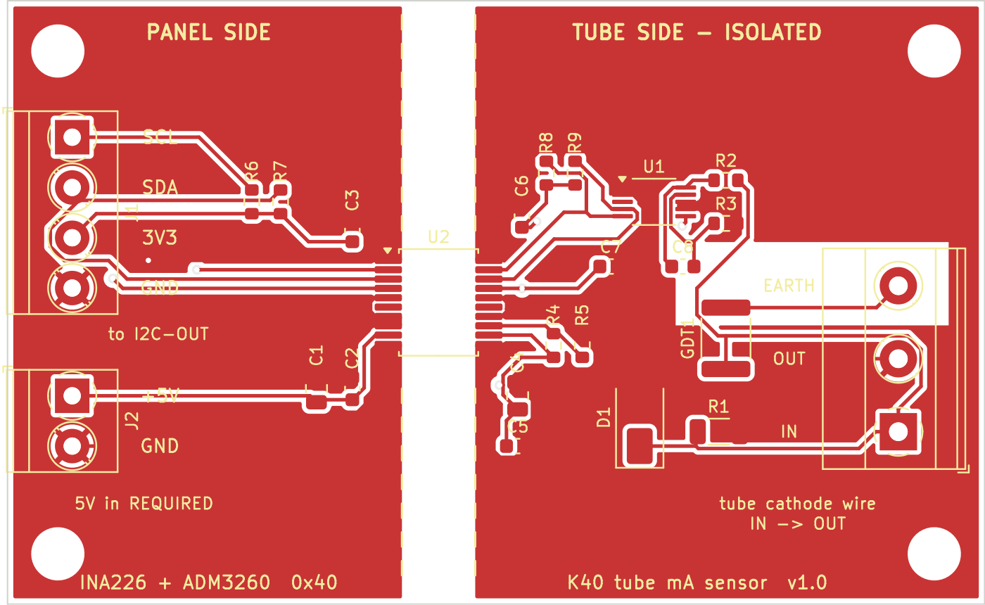 | 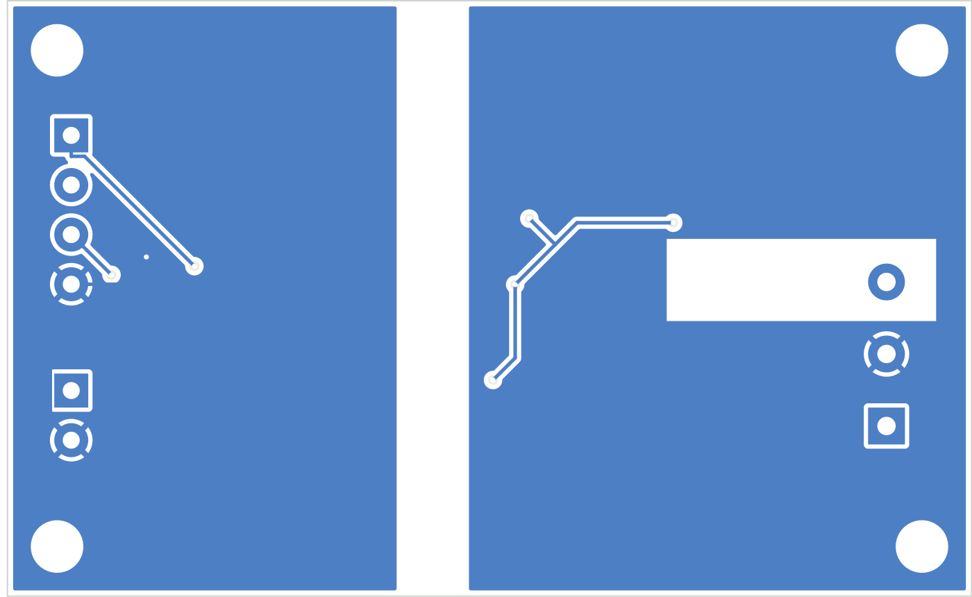 |
| Terminal | Pin | Goes to |
|---|---|---|
| J1 (3.5 mm, 4-pin) | SCL, SDA, 3V3, GND | Panel I2C-OUT (Grove cable, cut one end; red = 3V3, black = GND, yellow = SCL, white = SDA) |
| J2 (3.5 mm, 2-pin) | +5V, GND | The 5 V supply (same 5 V that feeds the panel's UART3-IN pin 3) |
| J3 (5.08 mm, 3-pin) | IN, OUT, EARTH | Tube cathode wire IN → OUT; EARTH to the chassis earth screw |
J2 must have 5 V. The isolated side runs at 5 V so the INA226 reads the ADM3260's logic levels reliably, and the ADM3260 can only make 5 V from a 5 V input.
 Panel side                         |  barrier  |   Tube side (isolated)
                                    |           |
 J1 SCL ──┬─ R6 4.7k ─ 3V3          |   U2      |          VISO (5 V)
 J1 SDA ──┼─ R7 4.7k ─ 3V3          | ADM3260   |   R8/R9 4.7k pull-ups to VISO
          └── SCL2/SDA2 ────────────┤ I2C + DC/DC├── SCL1/SDA1 ─── U1 INA226 (0x40)
 J1 3V3 ── VDDP (C3 100n)           |           |   VISO ── U1 VS (C7 100n)
 J2 +5V ── VIN  (C1 10u, C2 100n)   |           |   VISO (C4 10u, C5 100n), VDDISO (C6 100n)
 PDIS ── GND (converter on)         |           |   VSEL: R4 30k / R5 10k  → 4.9 V
                                    |           |
                                    |           |   J3 IN ─┬─ R1 0.1 Ω ─┬─ J3 OUT (= isolated GND)
                                    |           |          ├ D1 SMAJ5.0CA ┤
                                    |           |          ├ R2 10 Ω ─ IN+ ┐ C8 100n
                                    |           |          │      R3 10 Ω ─ IN− ┘
                                    |           |          └ GDT1 200 V ── J3 EARTH
Full netlist (checked against the board file):
| Net | Pins |
|---|---|
| +3V3 | J1.3, U2.4 VDDP, C3, R6, R7 |
| +5V | J2.1, U2.9 VIN, C1, C2 |
| GND | J1.4, J2.2, U2.1/5/7/10, U2.8 PDIS, C1, C2, C3 |
| SCL_P / SDA_P | J1.1 / J1.2, U2.2 SCL2 / U2.3 SDA2, R6 / R7 |
| VISO | U2.12 VISO, U2.17 VDDISO, U1.6 VS, C4–C7, R4, R8, R9 |
| VSEL | U2.13, R4/R5 junction |
| SCL_I / SDA_I | U2.19 SCL1 / U2.18 SDA1, U1.5 / U1.4, R8 / R9 |
| GNDISO | J3.2 OUT, U2.11/14/16/20, U1.1 A1, U1.2 A0, U1.7 GND, U1.8 VBUS, R1, R3, R5, D1, C4–C7 |
| TUBE_IN | J3.1 IN, R1, R2, D1, GDT1 |
| INP_F / INN_F | U1.10 IN+ / U1.9 IN−, R2 / R3, C8 |
| EARTH | J3.3, GDT1 |
fab/k40-current-sensor-gerbers.zip.
Defaults are fine: 2 layers, 1.6 mm, any color, HASL lead-free (or ENIG).fab/k40-current-sensor-bom.csv and fab/k40-current-sensor-cpl.csv.OSH Park also takes the same Gerber zip, but it doesn't assemble. You'd hand-solder the SSOP-20 and the 0.5 mm-pitch VSSOP-10 yourself.
| Ref | Part | Phoenix # |
|---|---|---|
| J1 | Screw terminal, 4-pos, 3.5 mm | PT 1,5/4-3,5-H 1984633 |
| J2 | Screw terminal, 2-pos, 3.5 mm | PT 1,5/2-3,5-H 1984617 |
| J3 | Screw terminal, 3-pos, 5.08 mm | MKDS 1,5/3-5,08 1715734 |
| – | Grove 4-pin cable (cut one end) to panel I2C-OUT | as in the module BOM |
| – | 4 × M3 nylon standoffs and screws | keeps the isolated side off the chassis |
| Ref | Value | Package | LCSC |
|---|---|---|---|
| U1 | INA226AIDGSR | VSSOP-10 | C49851 |
| U2 | ADM3260ARSZ | SSOP-20 | C208558 |
| R1 | 0.1 Ω 1 % 1 W (FOJAN FRM121WFR100TM) | 1206 | C7467250 |
| R2, R3 | 10 Ω | 0603 | C22859 |
| R4 | 30 kΩ | 0603 | C22984 |
| R5 | 10 kΩ | 0603 | C25804 |
| R6–R9 | 4.7 kΩ | 0603 | C23162 |
| C1, C4 | 10 µF 25 V | 0805 | C15850 |
| C2, C3, C5–C8 | 100 nF | 0603 | C14663 |
| D1 | SMAJ5.0CA bidirectional TVS | SMA | C10756 |
| GDT1 | 200 V gas discharge tube (Brightking 4532-201-LF; alt. 150 V 4532-151-LF C84727) | 1812 | C522630 |
Notes:
Cheaper than JLC assembly if you're OK hand-soldering fine-pitch SMT.
fab/k40-current-sensor-gerbers.zip to JLCPCB with assembly off
(about $2–5 for 5 boards plus shipping), or to OSH Park (about $22 for 3, shipped in the US).bom-digikey-arrow.csv to Digi-Key's BOM Manager (myLists → Upload) or
Arrow's BOM tool. The resistors and capacitors carry Digi-Key cut-tape part numbers
(the CT-ND / -1-ND ones), so you can buy 10 instead of a 5,000-piece reel. If any line
still matches a reel, switch its packaging to Cut Tape. The other parts are matched by
manufacturer part number, which Arrow also accepts. Quantities are
for 2 boards, with 10 of each small resistor and capacitor because they're easy to lose.
Expect roughly $45–60 total; most of that is the two ADM3260s (about $13–16 each).GDT1 here is the Yageo 4532-231-LF (230 V); any 1812-size GDT from 150 to 250 V fits the same pads.
A 3D-printable two-part box is in enclosure/ (STL files plus the OpenSCAD source).
| Path | What |
|---|---|
k40-current-sensor.kicad_pcb / .kicad_pro | KiCad 7 board (opens in KiCad 7 or 8) |
fab/k40-current-sensor-gerbers.zip | Gerbers and drill files for any fab |
fab/k40-current-sensor-bom.csv, -cpl.csv | JLCPCB assembly files |
drc.rpt | KiCad DRC: 0 clearance errors, 0 unconnected. Only notes are the terminal silkscreen past the board edge and "library not in table" |
tools/ | The scripts that generated the board (parts.py is the parts list and netlist) |
To regenerate after editing tools/parts.py:
cd tools
python3 build.py place                 # board + Specctra DSN
xvfb-run java -jar freerouting-1.9.0.jar -de board.dsn -do board.ses -mp 40
python3 build.py finish                # import routes, pour grounds
python3 export.py # Gerbers, BOM, CPL| Qty | Value | Footprint | References |
|---|---|---|---|
| 6 | 100nF | Capacitor_SMD:C_0603_1608Metric | C2, C3, C5, C6, C7, C8 |
| 4 | 4.7k | Resistor_SMD:R_0603_1608Metric | R6, R7, R8, R9 |
| 4 | MountingHole_3.2mm_M3 | MountingHole_3.2mm_M3 | H1, H2, H3, H4 |
| 2 | 10R | Resistor_SMD:R_0603_1608Metric | R2, R3 |
| 2 | 10uF 25V | Capacitor_SMD:C_0805_2012Metric | C1, C4 |
| 1 | 0.1R 1% 1206 1W | Resistor_SMD:R_1206_3216Metric | R1 |
| 1 | 10k | Resistor_SMD:R_0603_1608Metric | R5 |
| 1 | 30k | Resistor_SMD:R_0603_1608Metric | R4 |
| 1 | 5V in | TerminalBlock_Phoenix:TerminalBlock_Phoenix_PT-1,5-2-3.5-H_1x02_P3.50mm_Horizontal | J2 |
| 1 | ADM3260ARSZ | Package_SO:SSOP-20_5.3x7.2mm_P0.65mm | U2 |
| 1 | GDT 230V 1812 | Resistor_SMD:R_1812_4532Metric | GDT1 |
| 1 | I2C to panel | TerminalBlock_Phoenix:TerminalBlock_Phoenix_PT-1,5-4-3.5-H_1x04_P3.50mm_Horizontal | J1 |
| 1 | INA226AIDGSR | Package_SO:VSSOP-10_3x3mm_P0.5mm | U1 |
| 1 | SMAJ5.0CA | Diode_SMD:D_SMA | D1 |
| 1 | Tube return | TerminalBlock_Phoenix:TerminalBlock_Phoenix_MKDS-1,5-3-5.08_1x03_P5.08mm_Horizontal | J3 |

anyshake/explorer
🌏 Detecting seismic wave using 3 geophones and 3-axis accelerometer, pack & send data to AnyShake Observer over RS232 / RS485 serial.

BYU-I-eBadge/e-badge
A hackable eBadge platform for students — a customizable, programmable electronics badge designed for hands-on learning and creative exploration throughout their academic journey.


ParadigmEngineering/igvc-2023-hardware
Intelligent Ground Vehicle Competition (Spring 2023) hardware for the Paradigm Engineering Student Group

victorstoica114/UWB_Module_ESP_IDF
ESP-IDF 6.0.2 firmware for the custom UWB Module V1.0 Rev.B, based on an ESP32-S3-WROOM-1-N16R8. The same application image runs on every module; persistent identity and runtime configuration select the role and active…

vincentchen18/polyphonic-synthesizer
a 2 octave pcb musical instrument!!! :)))
It measures 68 × 42 mm and has 2 copper layers, 1.6 mm thick.
28 parts, built around the INA226AIDGSR, ADM3260ARSZ and SMAJ5.0CA. The full list of its parts is on this page, with links to each part's symbol and footprint where PCBKit's library has them.
From the MikonosII/k40-laser-panel repository on GitHub, at the commit this page was made from: the board is hardware/current-sensor-pcb/k40-current-sensor.kicad_pcb. PCBKit opens the board in the browser, with nothing to install.
Its repository states no licence, so its author keeps all rights: ask MikonosII before reusing the design.