2 layers45 × 45 mm

 MikkoTervala/lighthouse
Lighthouse for family connection
Panelized lighthouse pcb is an open-source printed circuit board by MikkoTervala, from the MikkoTervala/lighthouse repository on GitHub. It is a 2-layer board of 106 × 106 mm with 300 parts on 164 nets, routed with 1,132 tracks and 172 vias.
It is built around the ESP32-C3-WROOM-02-H4, CN5711 and AP2112K-3.3, with the USBLC6-2SC6 and WS2812B among its other parts. Its parts include 48 diodes, 44 resistors, 36 capacitors, 16 ICs and 12 switches. It belongs with the ESP32 and RISC-V boards of this library.


Lighthouse is a connected smart decoration that synchronizes over the internet to let your family know when you're home.
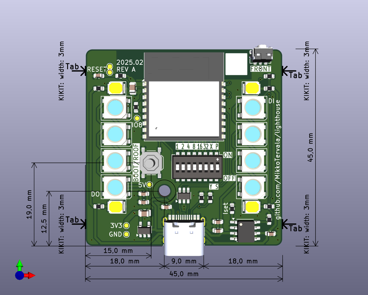
| Qty | Value | Footprint | References |
|---|---|---|---|
| 104 | NPTH | NPTH | KiKit_MB_10_1, KiKit_MB_10_2, KiKit_MB_10_3, KiKit_MB_10_4, KiKit_MB_10_5, KiKit_MB_11_1, KiKit_MB_11_2, KiKit_MB_11_3, KiKit_MB_11_4, KiKit_MB_11_5, KiKit_MB_12_1, KiKit_MB_12_2, KiKit_MB_12_3, KiKit_MB_12_4, KiKit_MB_12_5, KiKit_MB_13_1 +88 |
| 32 | WS2812B | LED_SMD:LED_WS2812B_PLCC4_5.0x5.0mm_P3.2mm | D2, D2, D2, D2, D11, D11, D11, D11, D12, D12, D12, D12, D13, D13, D13, D13 +16 |
| 16 | 10k | Resistor_SMD:R_0603_1608Metric | R1, R1, R1, R1, R2, R2, R2, R2, R3, R3, R3, R3, R13, R13, R13, R13 |
| 16 | 2 | Resistor_SMD:R_0603_1608Metric | R7, R7, R7, R7, R8, R8, R8, R8, R9, R9, R9, R9, R10, R10, R10, R10 |
| 16 | 2.2µf | Capacitor_SMD:C_0603_1608Metric | C4, C4, C4, C4, C5, C5, C5, C5, C8, C8, C8, C8, C9, C9, C9, C9 |
| 16 | LED 0.5W 3000k | lighthouse_footprints:LED_PLCC_2835 | D7, D7, D7, D7, D8, D8, D8, D8, D9, D9, D9, D9, D10, D10, D10, D10 |
| 8 | 10µf | Capacitor_SMD:C_0805_2012Metric | C3, C3, C3, C3, C6, C6, C6, C6 |
| 8 | 220nf | Capacitor_SMD:C_0603_1608Metric | C7, C7, C7, C7, C10, C10, C10, C10 |
| 8 | 5.1k | Resistor_SMD:R_0603_1608Metric | R5, R5, R5, R5, R6, R6, R6, R6 |
| 8 | Fiducial | Fiducial | KiKit_FID_B_1, KiKit_FID_B_2, KiKit_FID_B_3, KiKit_FID_B_4, KiKit_FID_T_1, KiKit_FID_T_2, KiKit_FID_T_3, KiKit_FID_T_4 |
| 8 | GND | TestPoint:TestPoint_Pad_D1.0mm | TP1, TP1, TP1, TP1, TP5, TP5, TP5, TP5 |
| 4 | 1µF | Capacitor_SMD:C_0603_1608Metric | C1, C1, C1, C1 |
| 4 | 3V3 | TestPoint:TestPoint_Pad_D1.0mm | TP2, TP2, TP2, TP2 |
| 4 | 3k | Resistor_SMD:R_0603_1608Metric | R11, R11, R11, R11 |
| 4 | 5V | TestPoint:TestPoint_Pad_D1.0mm | TP6, TP6, TP6, TP6 |
| 4 | AP2112K-3.3 | Package_TO_SOT_SMD:SOT-23-5 | U3, U3, U3, U3 |
| 4 | BOOT/ROOF | lighthouse_footprints:SW_Push_1P1T_XKB_TS-1187A | SW1, SW1, SW1, SW1 |
| 4 | CN5711 | Package_SO:SOIC-8-1EP_3.9x4.9mm_P1.27mm_EP2.41x3.3mm | U2, U2, U2, U2 |
| 4 | ESP32-C3-WROOM-02 | lighthouse_footprints:ESP32-C3-WROOM-02 | U1, U1, U1, U1 |
| 4 | FRONT | lighthouse_footprints:SW_Push_1P1T-MP_NO_Horizontal_Alps_SKRTLAE010 | SW3, SW3, SW3, SW3 |
| 4 | IO8 | TestPoint:TestPoint_Pad_D1.0mm | TP4, TP4, TP4, TP4 |
| 4 | MountingHole M2.5 | lighthouse_footprints:MountingHole_2.7mm_M2.5 | H4, H4, H4, H4 |
| 4 | RESET | lighthouse_footprints:TestPoint_Pad_D1.0mm_no_court | TP3, TP3, TP3, TP3 |
| 4 | SW_DIP_x08 | Button_Switch_SMD:SW_DIP_SPSTx08_Slide_Copal_CHS-08A_W5.08mm_P1.27mm_JPin | SW4, SW4, SW4, SW4 |
| 4 | USBLC6-2SC6 | Package_TO_SOT_SMD:SOT-23-6 | U4, U4, U4, U4 |
| 4 | USB_C_Receptacle_USB2.0 | lighthouse_footprints:USB_C_Receptacle_HRO_TYPE-C-31-M-12 | J1, J1, J1, J1 |


joshitha-c/rf_detector
A portable, custom-built RF signal scanner and power detector designed for knowing wireless signals, measuring signal strength and can be used to be safe.

Wassasin/leddimmer
Quick low-side PWM device to crudely dim two 24V 4A LED strips

pushtiujeniya/ESP32-C3-WROOM02_dev-board
This project is a custom 2-layer development board designed around the ESP32-C3-WROOM-02 Wi‑Fi + Bluetooth MCU module.


anasskrim61-wq/esp32-c3-mini
Custom ESP32-C3 Mini IoT hardware design and KiCad PCB project

bapsenpai-blip/STM32F405-4-layer-flight-controller
My first PCB revision, not fabricated yet, looking for design review
It measures 106 × 106 mm and has 2 copper layers, 1.6 mm thick.
300 parts, built around the ESP32-C3-WROOM-02-H4, CN5711, AP2112K-3.3 and USBLC6-2SC6. The full list of its parts is on this page, with links to each part's symbol and footprint where PCBKit's library has them.
From the MikkoTervala/lighthouse repository on GitHub, at the commit this page was made from: the board is pcb/panelize/panelized-lighthouse-pcb.kicad_pcb and its schematic pcb/lighthouse-pcb.kicad_sch. PCBKit opens the board in the browser, with nothing to install.
Its repository states no licence, so its author keeps all rights: ask MikkoTervala before reusing the design.