4 layers28 × 65 mm
 MicroType-Engineering/YouTube_Projects
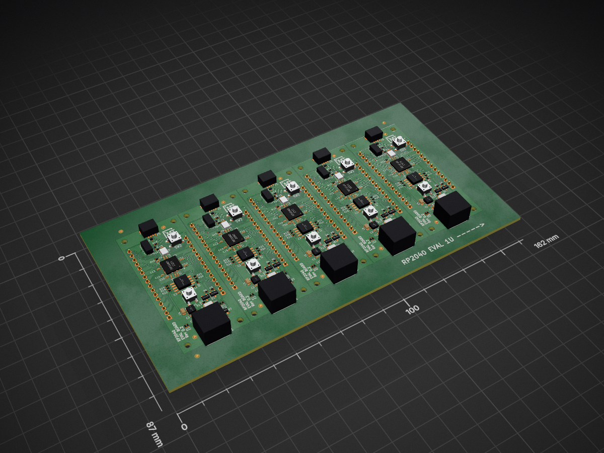
RP2040 Eval Board is an open-source printed circuit board by MicroType-Engineering, from the MicroType-Engineering/YouTube_Projects repository on GitHub, published under the MIT licence. It is a 4-layer board of 162 × 87 mm with 321 parts on 425 nets, routed with 3,195 tracks and 350 vias.
It is built around the RP2040, ST1L05APU33R and CC0402KRX5R7BB105, with the BSS138K, ESD7L5.0DT5G and PTS 647 SN38 SMTR2 LFS among its other parts. Its parts include 110 resistors, 80 capacitors, 25 connectors, 20 diodes and 15 ICs. It belongs with the RP2040 boards of this library.


| Qty | Value | Footprint | References |
|---|---|---|---|
| 70 | CC0402KRX5R7BB105 | footprints:CAPACITOR_0402N | C10, C10, C10, C10, C10, C11, C11, C11, C11, C11, C12, C12, C12, C12, C12, C13 +54 |
| 55 | RC0402FR-0727RL | footprints:RESISTOR_0402N | R16, R16, R16, R16, R16, R17, R17, R17, R17, R17, R18, R18, R18, R18, R18, R19 +39 |
| 20 | RC0402JR-07510RL | footprints:RESISTOR_0402N | R8, R8, R8, R8, R8, R9, R10, R10, R10, R10, R10, R13, R13, R13, R13, R13 +4 |
| 15 | BSS138K | footprints:SOT23-3P95_285X115L45X42N | Q1, Q1, Q1, Q1, Q1, Q2, Q2, Q2, Q2, Q2, Q3, Q3, Q3, Q3, Q3 |
| 10 | ESD7L5.0DT5G | footprints:DIOSOFL3P40_120X120X55L29X21N | D1, D1, D1, D1, D1, D3, D3, D3, D3, D3 |
| 10 | GRM21BR61H475KE51L | footprints:CAPACITOR_0805N | C1, C1, C1, C1, C1, C4, C4, C4, C4, C4 |
| 10 | PTS_647_SN38_SMTR2_LFS | footprints:PTS_647_SN70_SMTR2_LFS | SW1, SW1, SW1, SW1, SW1, SW2, SW2, SW2, SW2, SW2 |
| 10 | RC0402JR-0710KL | footprints:RESISTOR_0402N | R14, R14, R14, R14, R14, R15, R15, R15, R15, R15 |
| 10 | RC0402JR-071KL | footprints:RESISTOR_0402N | R11, R11, R11, R11, R11, R12, R12, R12, R12, R12 |
| 10 | RC0402JR-075K1L | footprints:RESISTOR_0402N | R1, R1, R1, R1, R1, R2, R2, R2, R2, R2 |
| 5 | 12401598E4#2A | footprints:12401598E4#2A | J1, J1, J1, J1, J1 |
| 5 | 150120RS75000 | footprints:LED_1206N | D4, D4, D4, D4, D4 |
| 5 | ASE-12.000MHZ-ET | footprints:OSCSC4P210_320X250X120L65X90N | X1, X1, X1, X1, X1 |
| 5 | CLVBA-FKA-CAEDH8BBB7A363 | footprints:CLVBA-FKA-CAEDH8BBB7A363N | D2, D2, D2, D2, D2 |
| 5 | DNP | footprints:RESISTOR_0402N | R3, R3, R3, R3, R3 |
| 5 | LOGO | footprints:MTE_LOGO_5MM | G***, G***, G***, G***, G*** |
| 5 | RP2040 | footprints:QFN57P40_700X700X90L40X18T310N | U3, U3, U3, U3, U3 |
| 5 | SM04B-SRSS-TB(LF)(SN) | footprints:SM04B-SRSS-TB(LF)(SN) | J5, J5, J5, J5, J5 |
| 5 | ST1L05APU33R | footprints:SON7P95_300X300X100L40X34T236X162N | U1, U1, U1, U1, U1 |
| 5 | Tag_Connect_Programmer_6-Pin | footprints:TC2030_SMALL_NO_LEGS | J2, J2, J2, J2, J2 |
| 5 | W25Q128JVSIM_TR | footprints:SOIC8P127_528X790X216L65X41N | U2, U2, U2, U2, U2 |
| 5 | _GENERIC_CONNECTOR_01x14 | Connector_PinHeader_2.54mm:PinHeader_1x14_P2.54mm_Vertical | J3, J3, J3, J3, J3 |
| 5 | _GENERIC_CONNECTOR_01x16 | Connector_PinHeader_2.54mm:PinHeader_1x16_P2.54mm_Vertical | J4, J4, J4, J4, J4 |
The 285 most common of 321 parts.


Mig-M27/Avionics-PCBs
Este repositório é usado para gerir as versões dos projetos KiCAD do sistema de Avionics da Porto Space Team. Está dividido em 2 secções: 1.


GarronAnderson/InsideMyHive-V2
an open-source bee box monitor, now low-power with (hopefully) better code


median-dispersion/GMT-Geiger-Counter
Geiger-Müller tube based Geiger counter.

It measures 162 × 87 mm and has 4 copper layers, 1.6 mm thick.
321 parts, built around the RP2040, ST1L05APU33R, CC0402KRX5R7BB105 and BSS138K. The full list of its parts is on this page, with links to each part's symbol and footprint where PCBKit's library has them.
From the MicroType-Engineering/YouTube_Projects repository on GitHub, at the commit this page was made from: the board is RP2040 Eval Board/panel/RP2040 Eval Board.kicad_pcb and its schematic Layout V Cap Test Board/Layout V Cap Test Board.kicad_sch. PCBKit opens the board in the browser, with nothing to install.
Its repository publishes it under the MIT licence: you may reuse it on that licence's terms (keep the author's notice, and for a copyleft licence share your changes alike).