
4 layers234 × 84 mm
Main panel
google/mozc-devices
Circuit diagrams and firmware source code for Gboard DIY keyboards
234 parts3kApache-2.0

 Matyas604/Matyas-s-Hackpad3
My first own project, which includes a PCB and 3D printed components that I made.
Matyas s Hackpad is an open-source printed circuit board by Matyas604, from the Matyas604/Matyas-s-Hackpad repository on GitHub, published under the MIT licence. It is a 2-layer board of 80 × 62.5 mm with 27 parts on 29 nets, routed with 261 tracks and 33 vias.
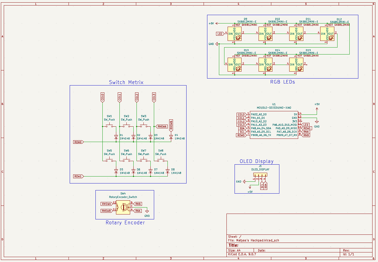
It is built around the SK6812MINI-E. Its parts include 15 diodes, 8 switches, 1 IC and 1 connector. It belongs with the keyboards and input boards of this library.
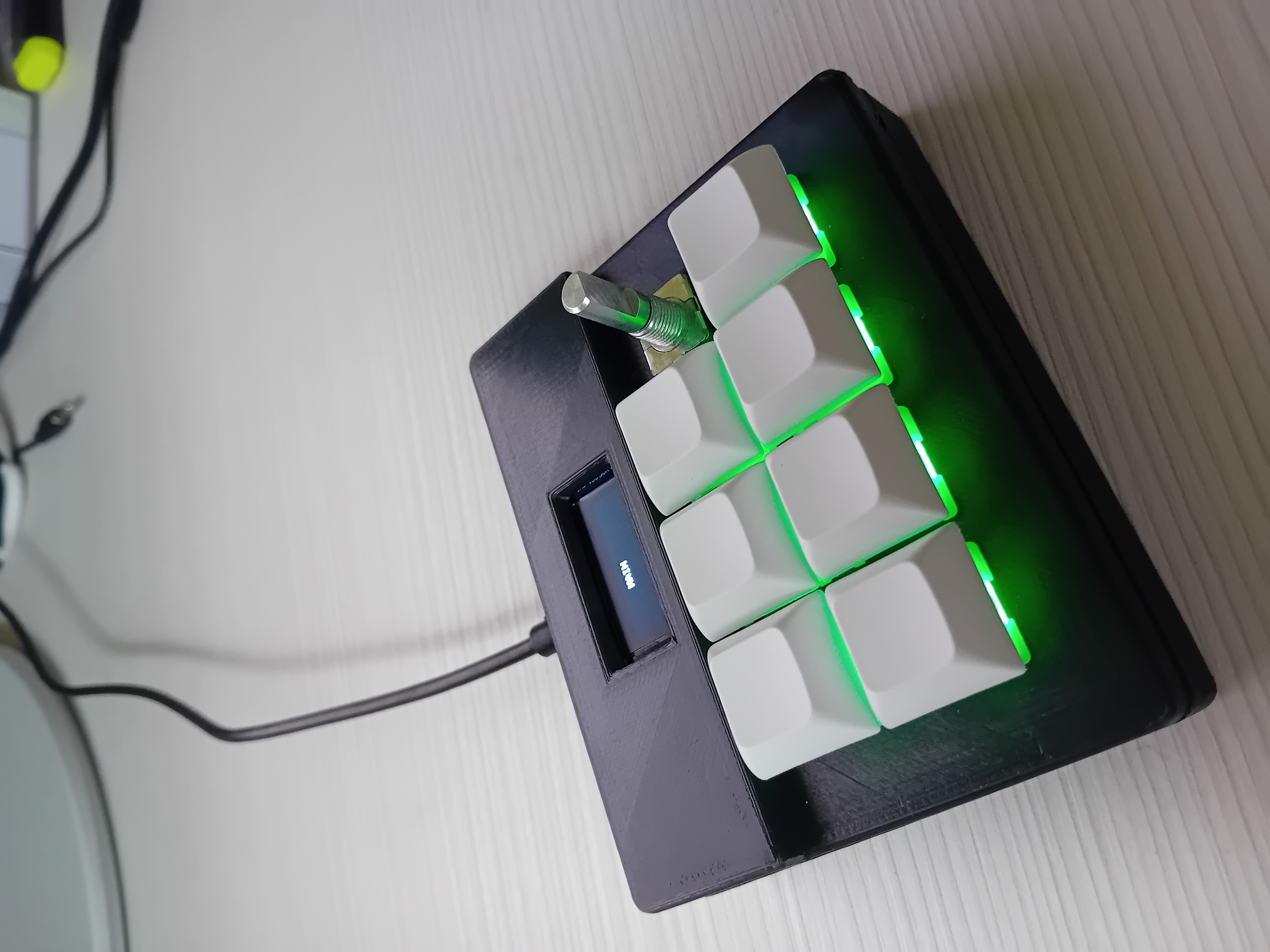
It has 8 keys (7 switches + rotary encoder switch), a rotary encoder, and an OLED display. Each key is backlit with SK6812 MINI-E LEDs. It uses QMK firmware and VIA.
Everything is connected by four M3x16mm screws and M3x5mx4mm heatset inserts. The case is printed in two parts, top and bottom.
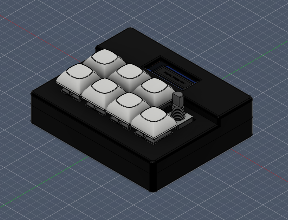
Made in Fusion360
Schematic
PCB
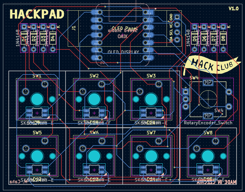
Made in KiCad
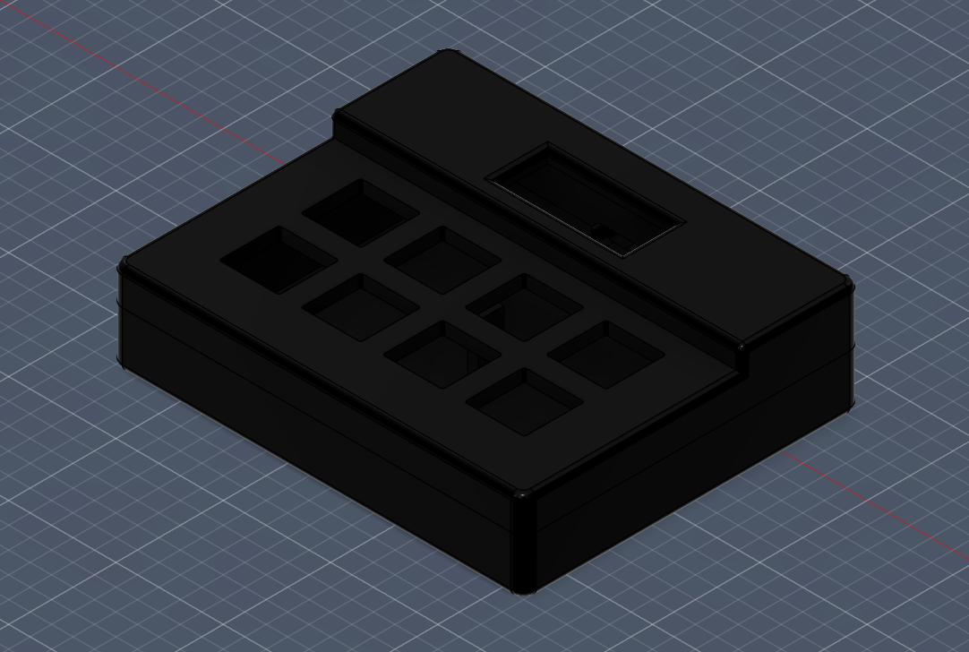
Made in Fusion360
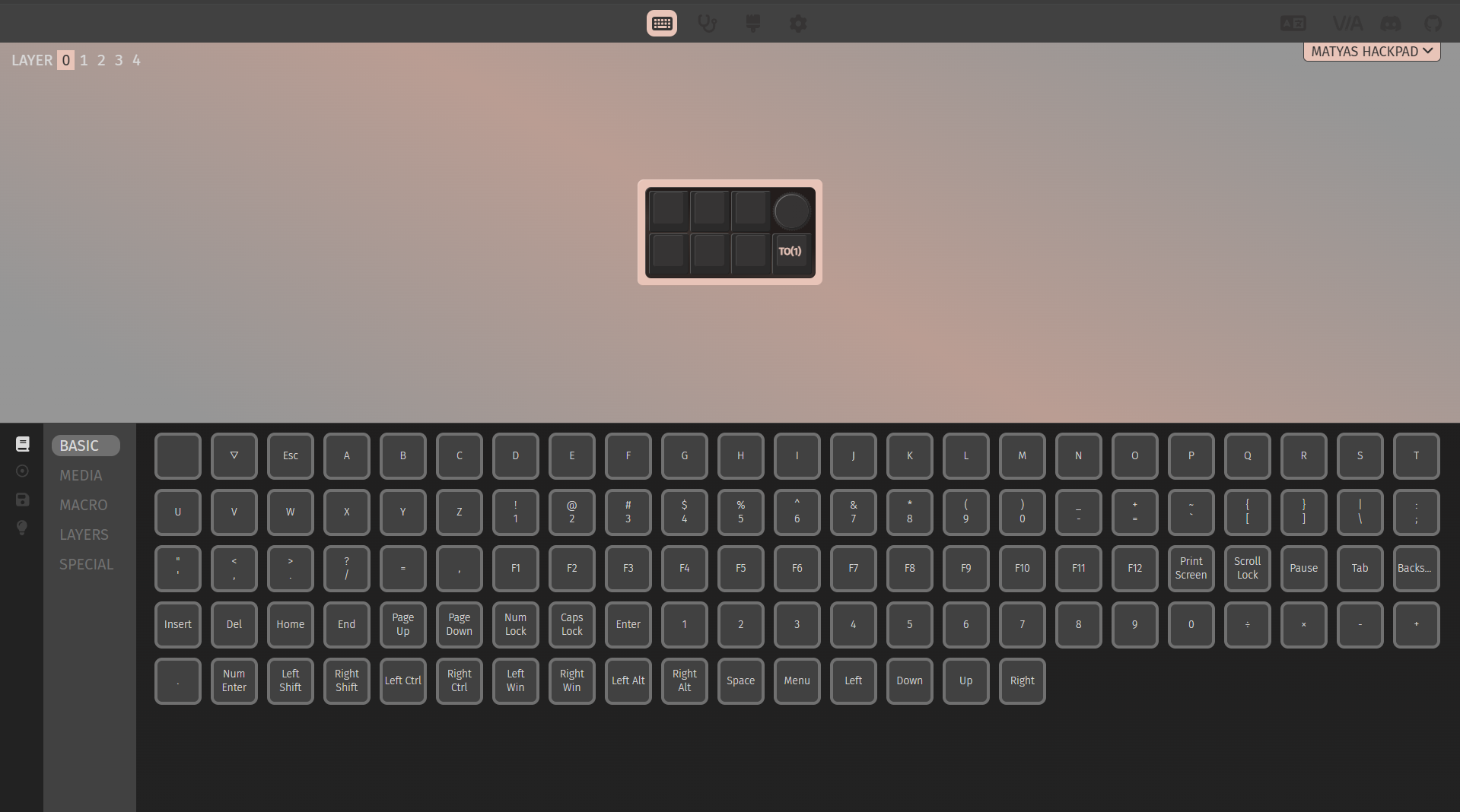
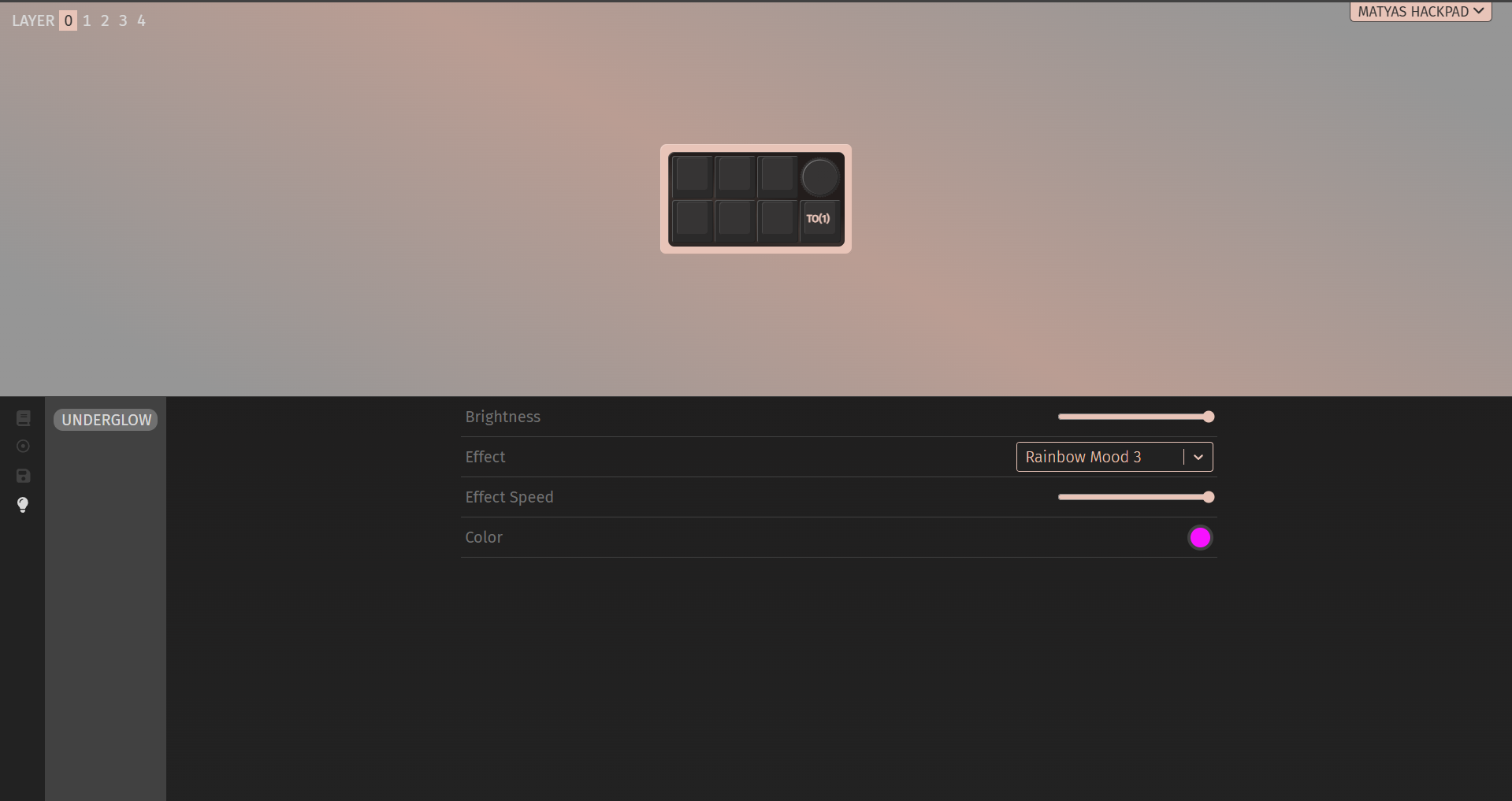
This Hackpad uses QMK firmware. Everything can be controlled in VIA. I have five layers set up, and I can assign anything to each one. I switch between them with a single switch. My layers are Main, Media, HA (shortcuts for Home Assistant), Game, and Other. I can also adjust the effects, speed, brightness, and backlight colors of LEDs directly from VIA. The OLED display shows the name of the current page.
Here is everything you need to create this Hackpad:
| Component | Amount |
|---|---|
| Seeed XIAO RP2040 | 1x |
| MX-Style switches | 7x |
| 1N4148 Diodes | 8x |
| EC11 Rotary encoder | 1x |
| 0.91 inch OLED display | 1x |
| DSA keycaps | 7x |
| SK6812 MINI-E LED | 7x |
| M3x16mm screw | 4x |
| M3x5mx4mm heatset insert | 4x |
| Case (2 printed parts) | 1x |
| PCB | 1x |
Made with ❤️ by @Matyas604
| Qty | Value | Footprint | References |
|---|---|---|---|
| 8 | 1N4148 | Diode_THT:D_DO-35_SOD27_P7.62mm_Horizontal | D1, D2, D3, D4, D5, D6, D7, D8 |
| 7 | SK6812MINI-E | footprints:SK6812MINI-E_fixed | D9, D10, D11, D12, D13, D14, D15 |
| 7 | SW_Push | Button_Switch_Keyboard:SW_Cherry_MX_1.00u_PCB | SW1, SW2, SW3, SW5, SW6, SW7, SW8 |
| 1 | clipboard:462f2333-586c-4cc8-b04d-9995b911b9d8 | ||
| 1 | clipboard:de5363f7-c900-46a6-94f2-35cc7d6a2b93 | ||
| 1 | MOUDLE-SEEEDUINO-XIAO | footprints:XIAO-Generic-Hybrid-14P-2.54-21X17.8MM | U1 |
| 1 | OLED_DISPLAY | footprints:SSD1306-0.91-OLED-4pin-128x32 | J1 |
| 1 | RotaryEncoder_Switch | Rotary_Encoder:RotaryEncoder_Alps_EC11E-Switch_Vertical_H20mm | SW4 |
google/mozc-devices
Circuit diagrams and firmware source code for Gboard DIY keyboards

Bastardkb/Dilemma
The Dilemma is a vertical stagger low-profile keyboard with mods.

Pwnsat/FlatSat
Flatsat v1.0 is a hardware based platform for aerospace cybersecurity research

adamws/kicad-kbplacer
KiCad plugin for automatic keyboard's key placement and routing

imchipwood/dumbpad
Simple 4x4 numpad with rotary encoder. Powered by QMK via ATmega32u4 Pro Micro

makerforgetech/modular-biped
An open source framework for creating a bipedal modular companion robot.


It measures 80 × 62.5 mm and has 2 copper layers, 1.6 mm thick.
27 parts, built around the SK6812MINI-E. The full list of its parts is on this page, with links to each part's symbol and footprint where PCBKit's library has them.
From the Matyas604/Matyas-s-Hackpad repository on GitHub, at the commit this page was made from: the board is PCB/Matyas's Hackpad.kicad_pcb and its schematic PCB/Matyas's Hackpad.kicad_sch. PCBKit opens the board in the browser, with nothing to install.
Its repository publishes it under the MIT licence: you may reuse it on that licence's terms (keep the author's notice, and for a copyleft licence share your changes alike).