2 layers346.2 × 95.5 mm

 Manawyrm/Gigaset-Debug-Adapter43
Gigaset-Debug-Adapter can be used with many Gigaset DECT phone models to access the internal UART. It's basically a 1.8V USB->UART converter, with switchable strapping logic and 3V step-down converter.
Gigaset Debug Adapter is an open-source printed circuit board by Manawyrm, from the Manawyrm/Gigaset-Debug-Adapter repository on GitHub, published under the GPL-3.0 licence. It is a 4-layer board of 20.7 × 40.2 mm with 54 parts on 49 nets, routed with 622 tracks and 94 vias.
It is built around the SY8088A, SRV05-4 and AO3400A, with the MMBT3904 among its other parts. Its parts include 18 resistors, 13 capacitors, 4 ICs, 4 diodes and 3 transistors. It belongs with the interfaces and adapters boards of this library.


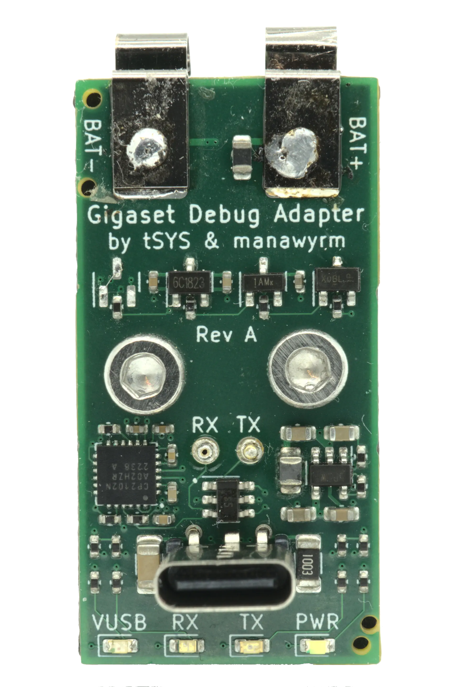
Gigaset-Debug-Adapter can be used with many Gigaset DECT phone models to access the internal UART.
It's basically a 1.8V USB->UART converter, with switchable strapping logic and 3V step-down converter.
dialog-cr16c-uart-boot can be used to upload a stub to the phone through the boot ROM and access the SPI NOR flash chip.
https://user-images.githubusercontent.com/748791/209271987-683d4506-6c61-477d-b1db-ebee4b655a7c.mp4
The PCB can (and should) be assembled at JLCPCBs assembly service.
Manufacturing files for the automatic assembly service can be found at gerbers/RevB/Gigaset-Debug-Adapter/.
JLC can probably also manufacture the 3D printed adapter for you, altough this was never tested. Please report if you do.
Additionally, you will need:
Note: We've had trouble soldering to the Keystone 5230 using lead-free solder! Use leaded solder instead.
sysmocom is making available a complete kit consisting of all the parts listed above which can be purchased via the sysmocom webshop
In order to enable the RX/TX LEDs, the internal EEPROM of the CP2102N USB->UART converter IC must be programmed to use the GPIO0 and GPIO1 pins as LED outputs. This can be done eiher
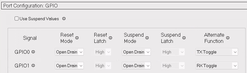
Simplicity Studio (and the experience of downloading it) is awful, be prepared and use a VM.
This step is fully optional, you just lose the LEDs. Those are pretty and useful, but not required.
The FOSS tool cp210x-program contains two separate programmers:
One python tool for CP2102, and the ext/badge/cp2102 C program which we need here.
Do something like
./bin/cp2102 -p "Gigaset Debug Adapter" -g onAnd then power-cycle the board to apply the new settings.
Schematic - Rev. B
Bootloader utility - dialog-cr16c-uart-boot
Rev.A: Bootloader Resistor logic is wrong, use Rev.B!
The battery adapter was designed using OpenSCAD. The definition file can be found as battery-adapter.scad.
OpenSCAD will generate a .stl file, suitable for 3D printing. This file can be converted for use in KiCad using meshconv:
meshconv -c wrl battery-adapter.stl -o battery-adapter| Qty | Value | Footprint | References |
|---|---|---|---|
| 4 | 4.7uF | Capacitor_SMD:C_0402_1005Metric | C2, C5, C11, C13 |
| 4 | 5.1k | Resistor_SMD:R_0402_1005Metric | R7, R11, R12, R15 |
| 3 | 100k | Resistor_SMD:R_0402_1005Metric | R9, R10, R13 |
| 3 | 100n | Capacitor_SMD:C_0402_1005Metric | C3, C4, C6 |
| 2 | 10k | Resistor_SMD:R_0402_1005Metric | R8, R14 |
| 2 | 10uF | Capacitor_SMD:C_0603_1608Metric | C7, C8 |
| 2 | 120k | Resistor_SMD:R_0402_1005Metric | R16, R18 |
| 2 | 22uF | Capacitor_SMD:C_0603_1608Metric | C10, C12 |
| 2 | 5.1 kR | Resistor_SMD:R_0402_1005Metric | R4, R5 |
| 2 | M3 Hole | MountingHole:MountingHole_3.2mm_M3 | H1, H2 |
| 2 | ToolingHole | ToolingHole:ToolingHole_JLCSMT | H3, H4 |
| 1 | 100k HV | Resistor_SMD:R_1206_3216Metric | R1 |
| 1 | 1nF | Capacitor_SMD:C_1206_3216Metric | C1 |
| 1 | 1uF | Capacitor_SMD:C_0402_1005Metric | C9 |
| 1 | 2.2uH | Inductor_SMD:L_0805_2012Metric_Pad1.15x1.40mm_HandSolder | L1 |
| 1 | 22k | Resistor_SMD:R_0402_1005Metric | R2 |
| 1 | 4.7k | Resistor_SMD:R_0402_1005Metric | R6 |
| 1 | 470k | Resistor_SMD:R_0402_1005Metric | R17 |
| 1 | 47k | Resistor_SMD:R_0402_1005Metric | R3 |
| 1 | 600R@100MHz | Inductor_SMD:L_0805_2012Metric | FB1 |
| 1 | AO3400A | Package_TO_SOT_SMD:SOT-23 | Q2 |
| 1 | BAT+ | Keystone5230:Keystone_5230 | TP3 |
| 1 | BAT- | Keystone5230:Keystone_5230 | TP4 |
| 1 | CP2102N-Axx-xQFN24 | Package_DFN_QFN:QFN-24-1EP_4x4mm_P0.5mm_EP2.6x2.6mm | U1 |
| 1 | DNP (AO3401A) | Package_TO_SOT_SMD:SOT-23 | Q3 |
| 1 | GRN (RX) | LED_SMD:LED_0603_1608Metric | D3 |
| 1 | LOGO | DECTPentagram:pentadect | G*** |
| 1 | MMBT3904 | Package_TO_SOT_SMD:SOT-23 | Q1 |
| 1 | RED (VBUS) | LED_SMD:LED_0603_1608Metric | D1 |
| 1 | RX | PogoPins:PogoPin_0.96mm | TP1 |
| 1 | SRV05-4 | Package_TO_SOT_SMD:SOT-23-6 | U2 |
| 1 | SY8088 | Package_TO_SOT_SMD:SOT-23-5 | U3 |
| 1 | TX | PogoPins:PogoPin_0.96mm | TP2 |
| 1 | USB_C_Receptacle | Connector_Jing:USB_Type_C_Straight_C168703 | J1 |
| 1 | WHT (VCC) | LED_SMD:LED_0603_1608Metric | D4 |
| 1 | XC6206P18xMR | Package_TO_SOT_SMD:SOT-23 | U4 |
| 1 | YLW (TX) | LED_SMD:LED_0603_1608Metric | D2 |

swayerloren/KICAD_ENGINE
AI-assisted KiCad PCB design workflow for schematics, PCB layouts, DRC, BOM/CPL, and fabrication outputs using Codex or Claude.

Kleavox/DeltaT32
Hardware design based on ESP32-C3 Mini-1, aiming for wearable and general-purpose use, with modular sensor separation.


yanghu/unicorne
A one-piece 40% ortho keyboard design inspired by crkbd, Kyria and Ferris.


VIPQualityPost/polarizer-illuminator
15W USB PD powered microscope illuminator with electrically controlled liquid crystal polarizer for removing specular reflections.

IM-TechieScientist/custom-stlink
A custom STLink compatible debugger using STM32F103 designed using KiCAD
It measures 20.7 × 40.2 mm and has 4 copper layers, 1.6 mm thick.
54 parts, built around the SY8088A, SRV05-4, AO3400A and MMBT3904. The full list of its parts is on this page, with links to each part's symbol and footprint where PCBKit's library has them.
From the Manawyrm/Gigaset-Debug-Adapter repository on GitHub, at the commit this page was made from: the board is Gigaset-Debug-Adapter.kicad_pcb and its schematic Gigaset-Debug-Adapter.kicad_sch. PCBKit opens the board in the browser, with nothing to install.
Its repository publishes it under the GPL-3.0 licence: you may reuse it on that licence's terms (keep the author's notice, and for a copyleft licence share your changes alike).