2 layers77.3 × 79.4 mm

 Lewis-mbui/door-lock-system
A collection of PCB design files for a PCB that interfaces a Raspberry Pi with a door lock system and NFC reader
LOCK SYSTEM is an open-source printed circuit board by Lewis-mbui, from the Lewis-mbui/door-lock-system repository on GitHub. It is a 2-layer board of 106 × 57.5 mm with 32 parts on 50 nets, routed with 256 tracks and 19 vias.
It is built around the LM2596S-ADJ, BC817 and SRD-05VDC-SL-C. Its parts include 8 resistors, 7 connectors, 4 capacitors, 4 diodes and 4 transistors. It belongs with the radio and wireless and interfaces and adapters boards of this library.


This project involved designing a custom PCB to interface a Raspberry Pi with a door lock system and an NFC reader.
The goal was to replace a prototype built using separate modules and stripboard wiring with a more reliable and compact PCB solution.
The original system:
We designed a single PCB that integrates:
This reduced wiring complexity and improved overall system organization.
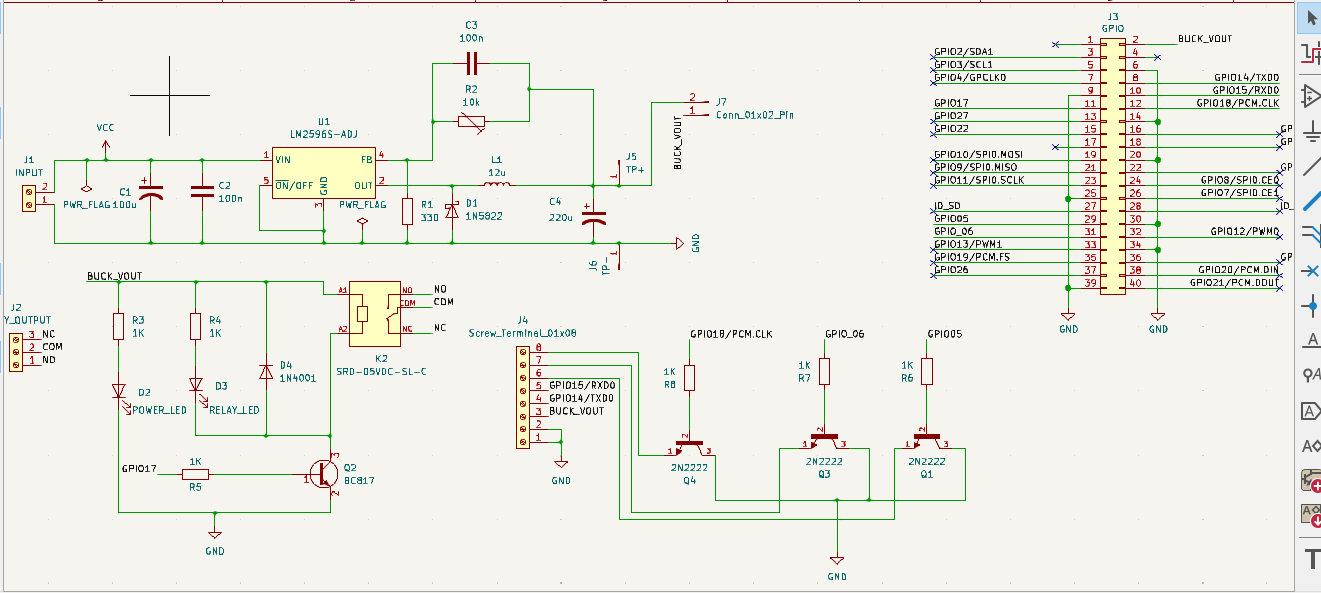
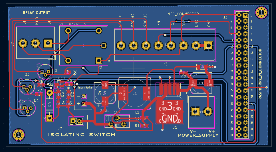
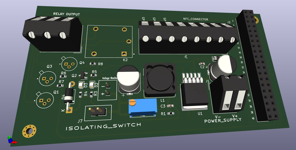
| Qty | Value | Footprint | References |
|---|---|---|---|
| 6 | 1K | Resistor_SMD:R_0603_1608Metric | R3, R4, R5, R6, R7, R8 |
| 3 | 2N2222 | 2N2222:TO127P584H533-3 | Q1, Q3, Q4 |
| 2 | 100n | Capacitor_SMD:C_0603_1608Metric_Pad1.08x0.95mm_HandSolder | C2, C3 |
| 1 | 100u | Capacitor_SMD:CP_Elec_8x10 | C1 |
| 1 | 10k | Potentiometer_THT:Potentiometer_Bourns_3296Y_Vertical | R2 |
| 1 | 12u | Inductor_SMD:L_Bourns_SRR1260 | L1 |
| 1 | 1N4001 | Diode_THT:D_DO-41_SOD81_P10.16mm_Horizontal | D4 |
| 1 | 1N5822 | Diode_SMD:D_1206_3216Metric | D1 |
| 1 | 220u | Capacitor_SMD:CP_Elec_8x10 | C4 |
| 1 | 330 | Resistor_SMD:R_0603_1608Metric_Pad0.98x0.95mm_HandSolder | R1 |
| 1 | BC817 | Package_TO_SOT_SMD:SOT-23 | Q2 |
| 1 | Conn_01x02_Pin | Connector_PinHeader_2.54mm:PinHeader_1x02_P2.54mm_Vertical | J7 |
| 1 | GPIO | Connector_PinSocket_2.54mm:PinSocket_2x20_P2.54mm_Vertical | J3 |
| 1 | INPUT | TerminalBlock_Altech:Altech_AK300_1x02_P5.00mm_45-Degree | J1 |
| 1 | LM2596S-ADJ | Package_TO_SOT_SMD:TO-263-5_TabPin3 | U1 |
| 1 | POWER_LED | LED_SMD:LED_0805_2012Metric | D2 |
| 1 | RELAY_LED | LED_SMD:LED_0805_2012Metric | D3 |
| 1 | RELAY_OUTPUT | TerminalBlock_Altech:Altech_AK300_1x03_P5.00mm_45-Degree | J2 |
| 1 | SRD-05VDC-SL-C | SRD-05VDC-SL-C:SRD-05VDC-SL-C | K2 |
| 1 | Screw_Terminal_01x08 | TerminalBlock_Altech:Altech_AK300_1x08_P5.00mm_45-Degree | J4 |
| 1 | TP+ | Connector_PinHeader_1.00mm:PinHeader_1x01_P1.00mm_Vertical | J5 |
| 1 | TP- | Connector_PinHeader_1.00mm:PinHeader_1x01_P1.00mm_Vertical | J6 |
The 30 most common of 32 parts.


Aleksei327/ESP32-C5-OBD2-Scanner
DIY dual-CAN OBD2 adapter on Seeed XIAO ESP32-C5 with a Flutter Android app. Working prototype, tested on a Citroën C3 II: full read-only ECU scan, PSA fault codes, live data. Single-sided home-etched KiCad board.


Pendu1699/solar-mppt-charge-controller
ESP32-based solar MPPT charge controller, custom PCB, perturb & observe tracking algorithm, logged efficiency test data.
It measures 106 × 57.5 mm and has 2 copper layers, 1.6 mm thick.
32 parts, built around the LM2596S-ADJ, BC817 and SRD-05VDC-SL-C. The full list of its parts is on this page, with links to each part's symbol and footprint where PCBKit's library has them.
From the Lewis-mbui/door-lock-system repository on GitHub, at the commit this page was made from: the board is LOCK_SYSTEM/LOCK_SYSTEM.kicad_pcb and its schematic LOCK_SYSTEM/LOCK_SYSTEM.kicad_sch. PCBKit opens the board in the browser, with nothing to install.
Its repository states no licence, so its author keeps all rights: ask Lewis-mbui before reusing the design.