
4 layers234 × 84 mm
Main panel
google/mozc-devices
Circuit diagrams and firmware source code for Gboard DIY keyboards
234 parts3kApache-2.0
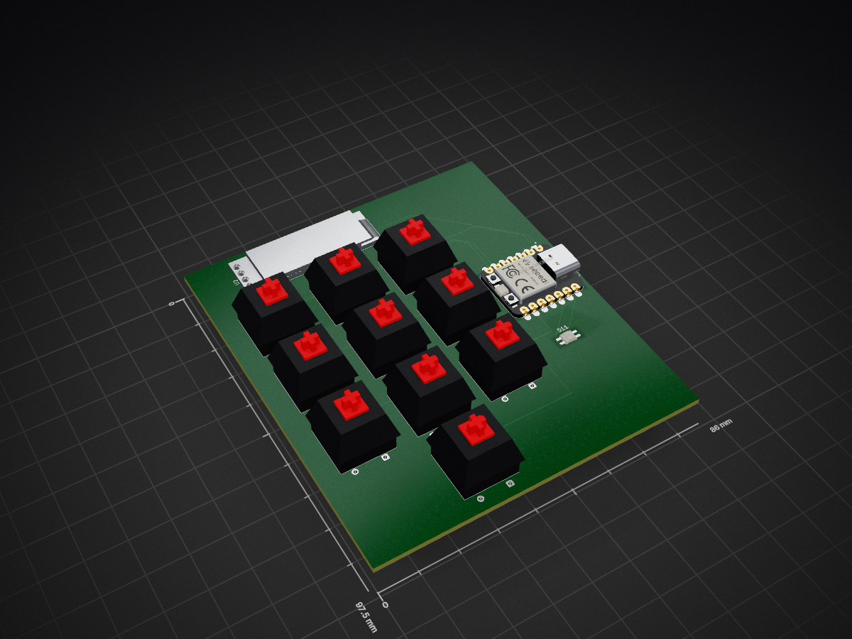
 Keyrajmnz/KeyraHackpad1
My first custom Hackpad: 10-key macropad with an OLED display, RGB LED, and XIAO RP2040.
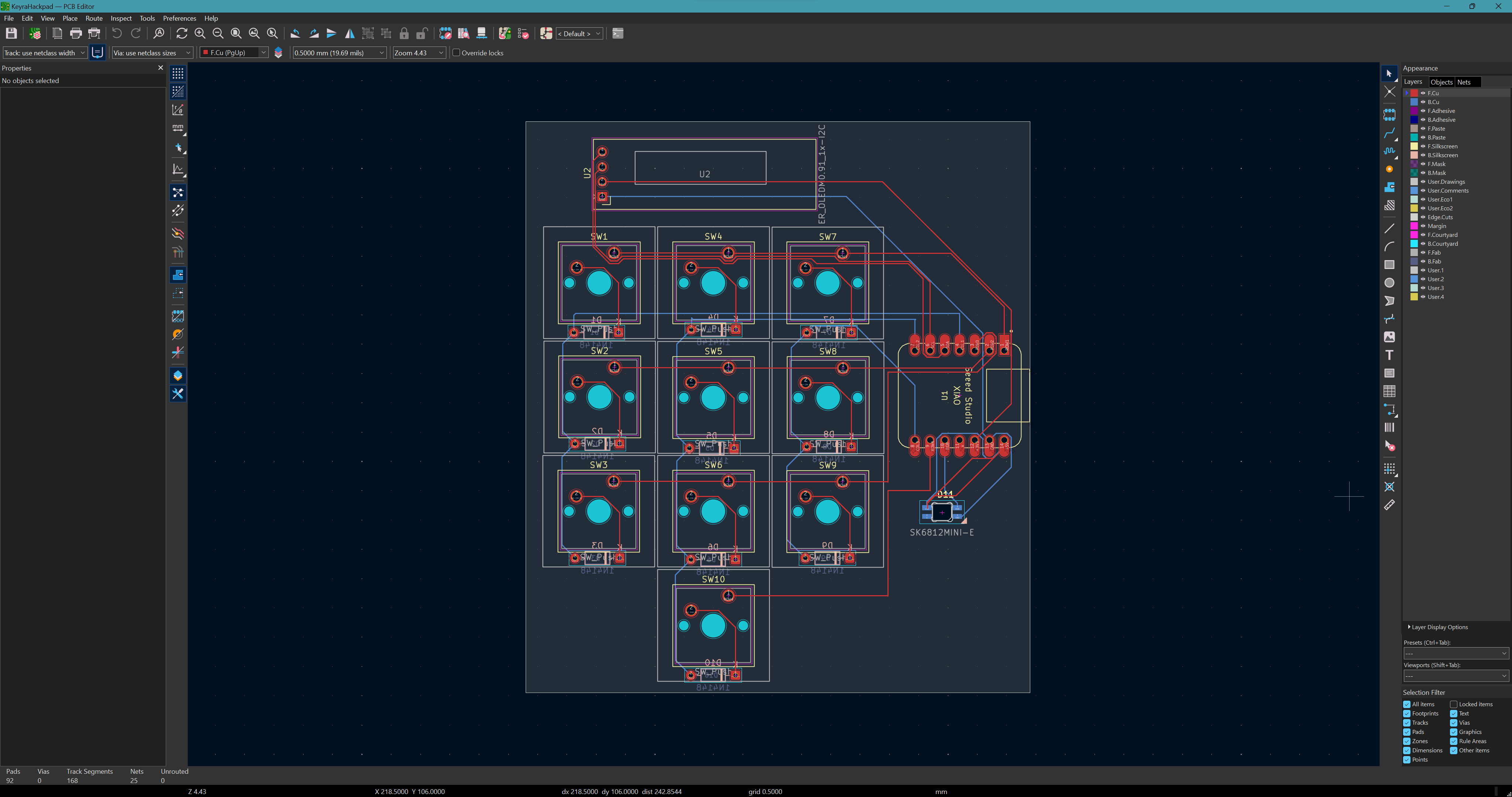
KeyraHackpad is an open-source printed circuit board by Keyrajmnz, from the Keyrajmnz/KeyraHackpad repository on GitHub. It is a 2-layer board of 86 × 97.5 mm with 23 parts on 25 nets, routed with 168 tracks and 0 vias.
It is built around the SK6812MINI-E. Its parts include 11 diodes, 10 switches and 2 ICs. It belongs with the lEDs and displays and keyboards and input boards of this library.
My first custom Hackpad: a 10-key macropad with an OLED display, RGB LED, and Seeed Studio XIAO RP2040.
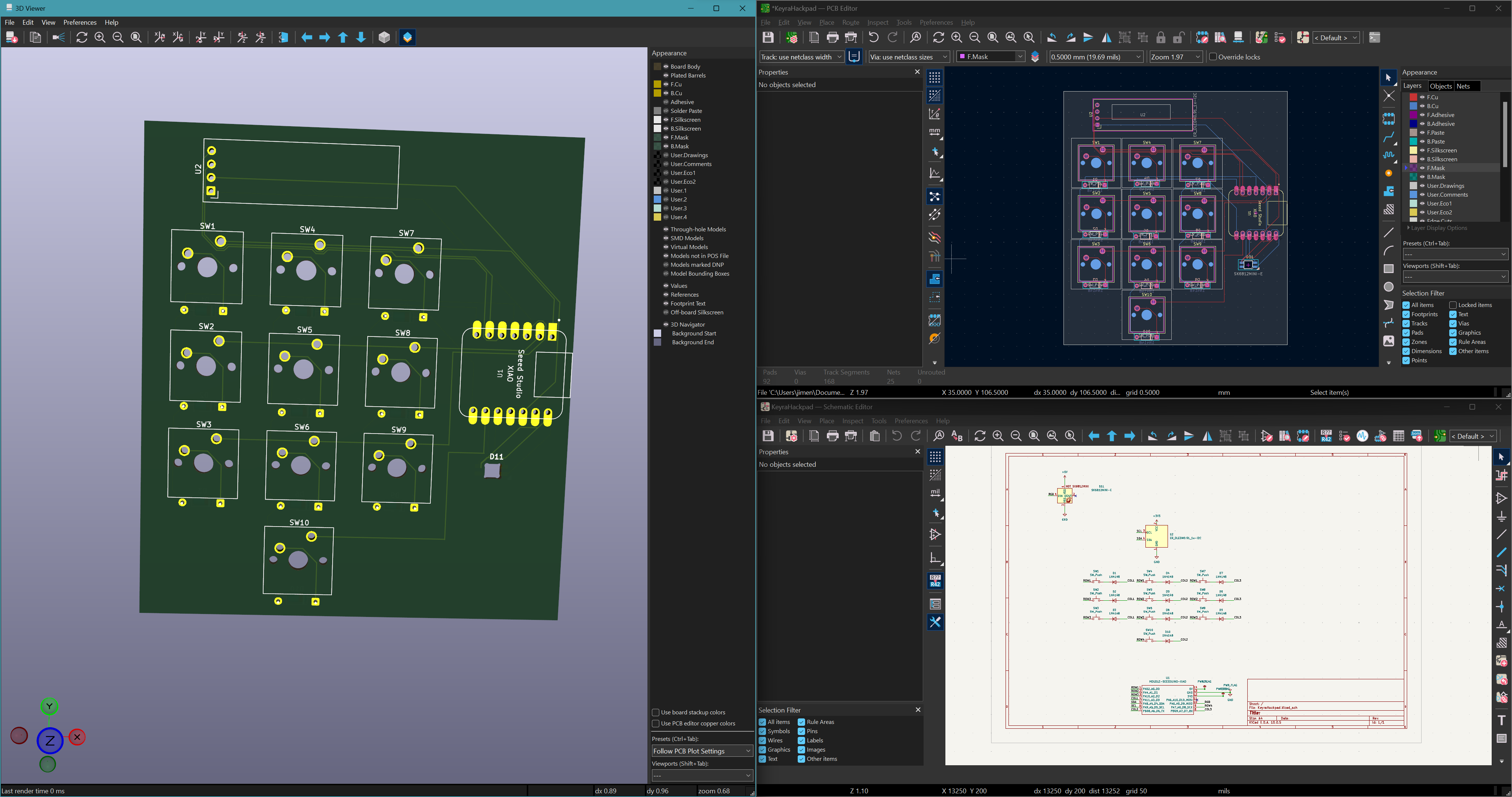
★ 10 mechanical keys
★ 0.91" 128×32 OLED display
★ SK6812MINI-E RGB LED
★ Seeed Studio XIAO RP2040
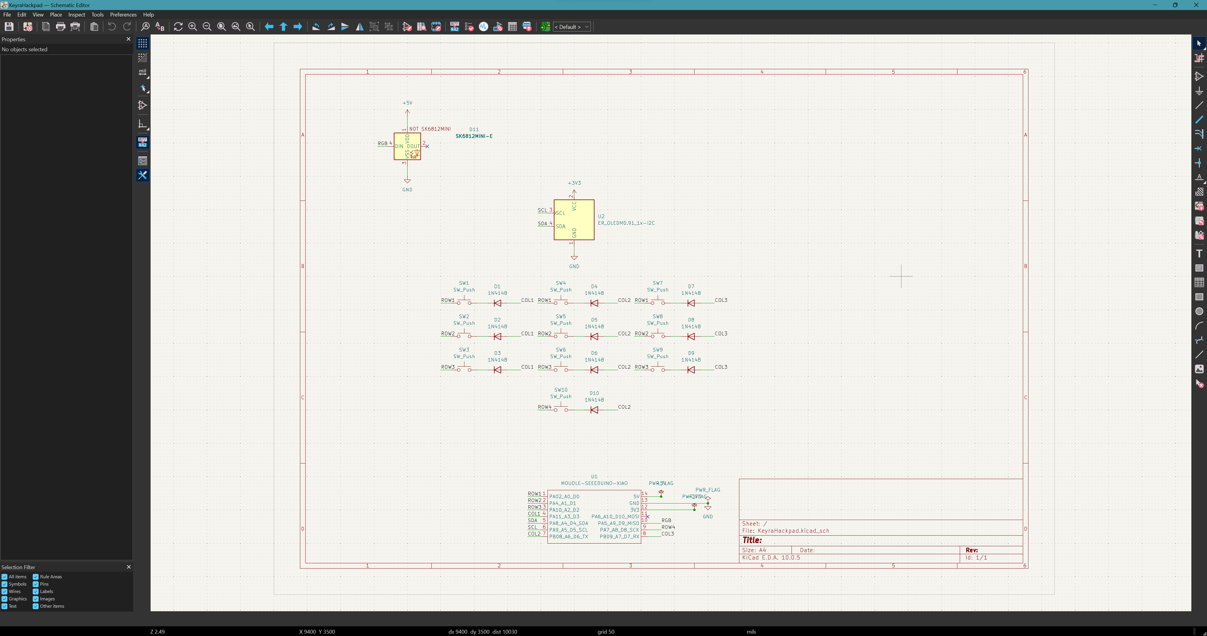
★ Custom PCB designed in KiCad
★ 4×3 switch matrix with 10 populated positions
★ Through-hole diodes for the switch matrix
★ Two firmware modes: Coding and Daily
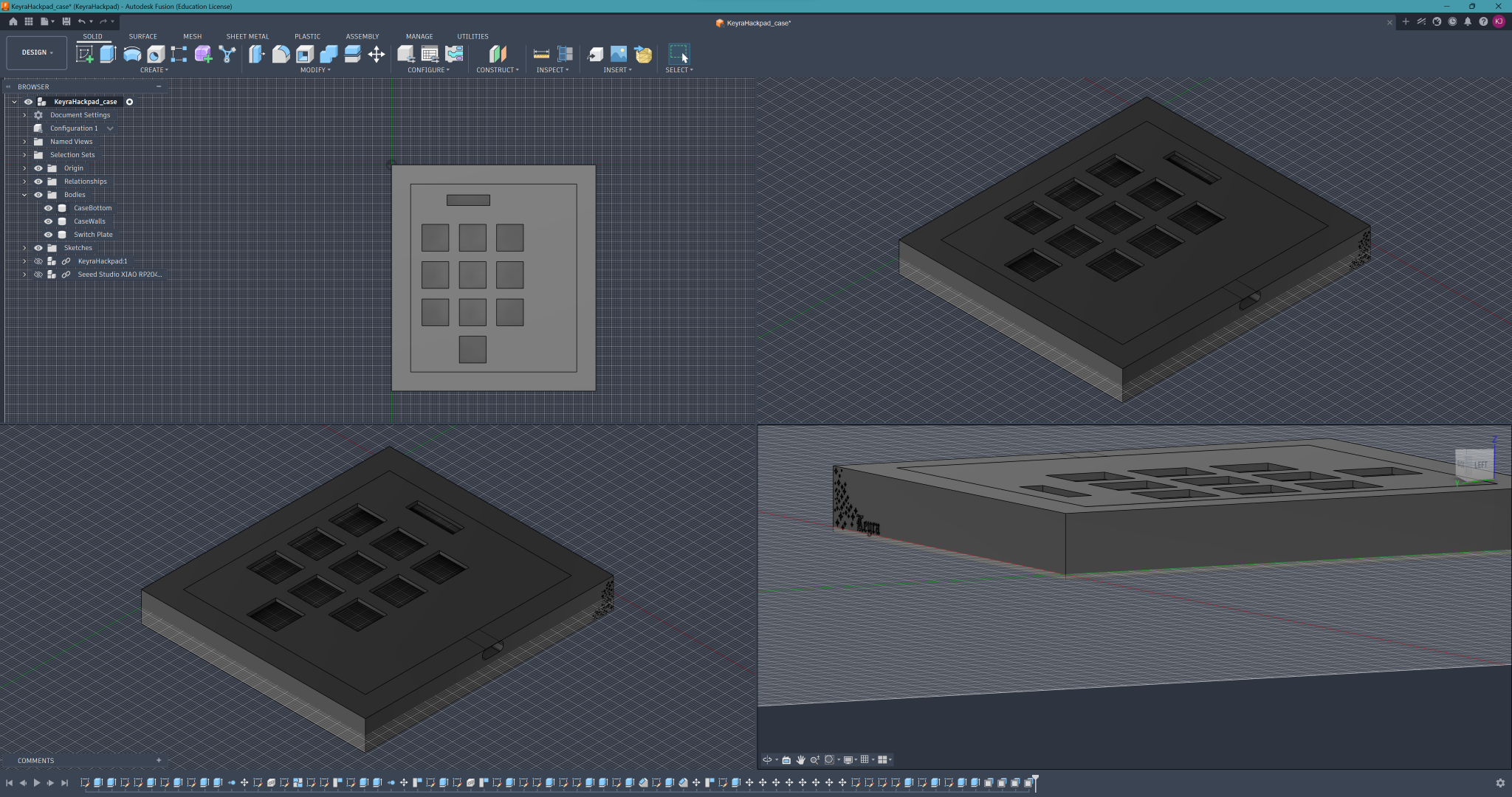
★ Custom Fusion 360 case
Coding Mode is designed for VS Code and includes:
★ Save — Ctrl + S
★ Undo — Ctrl + Z
★ Redo — Ctrl + Y
★ Copy — Ctrl + C
★ Paste — Ctrl + V
★ Screenshot — Win + Shift + S
★ Delete Line — Ctrl + Shift + K
★ Duplicate Line — Shift + Alt + Down
★ Find — Ctrl + F
Daily Mode provides quick access to:
★ Gmail
★ Canvas
★ GitHub
★ Google Calendar
★ ClassLink
★ Screenshot
★ Google Classroom
★ Highline Portal
★ ChatGPT
The bottom-center key switches between Coding Mode and Daily Mode.
The OLED displays the current mode, and the RGB LED changes color to indicate the active mode.
I designed the schematic and PCB in KiCad. I wired the 10-key switch matrix, connected the XIAO, OLED, and RGB LED, routed the PCB, checked the design, and exported the Gerber files for manufacturing.
The case was designed in Fusion 360 and exported as printable 3MF files and a STEP assembly.
The firmware is written in CircuitPython using KMK.
It includes:
★ 10-key matrix scanning
★ Coding Mode
★ Daily Mode
★ Mode switching
★ Keyboard shortcuts
★ Website shortcuts
★ OLED mode display
★ RGB mode indication
Firmware source:
Firmware/code.py
| Qty | Component | Notes |
|---|---|---|
| 10 | Cherry MX-compatible mechanical switches | 1.00u PCB mount |
| 10 | 1N4148 diodes | Through-hole, DO-35 |
| 1 | Seeed Studio XIAO RP2040 | Microcontroller |
| 1 | SK6812MINI-E | RGB LED |
| 1 | 0.91" 128×32 OLED display | I²C |
| 10 | MX-compatible keycaps | One per switch |
| 1 | 3D-printed case | Custom Fusion 360 design |
This was my first hardware project, so there was definitely a lot I had to figure out along the way.
★ I learned how to design a schematic and PCB in KiCad.
★ I learned how switch matrices, diodes, and microcontrollers work together.
★ I learned how to route a PCB and fix DRC issues.
★ I learned how to design a custom case in Fusion 360.
★ I learned how to create Gerber files for manufacturing.
★ I learned how to write CircuitPython firmware with KMK.
★ I learned how the PCB, case, OLED, RGB LED, and firmware all come together to make one project.
★ The hardest part for me was definitely the case in Fusion 360. I got stuck a lot and honestly wanted to give up at one point, but I kept working through the problems and eventually got the case to fit.
★ This project taught me that debugging and being patient are just as important as knowing how to code.
KeyraHackpad/
├── CAD/
│   └── KeyraHackpad_Case.step
│
├── PCB/
│   ├── KeyraHackpad.kicad_pcb
│   ├── KeyraHackpad.kicad_pro
│   └── KeyraHackpad.kicad_sch
│
├── Firmware/
│   └── code.py
│
├── production/
│   ├── CaseBottom.3mf
│   ├── Casewalls.3mf
│   ├── KeyraHackpad-Gerbers.zip
│   ├── main.py
│   └── SwitchPlatee.3mf
│
└── README.md| Qty | Value | Footprint | References |
|---|---|---|---|
| 10 | 1N4148 | Diode_THT:D_DO-35_SOD27_P7.62mm_Horizontal | D1, D2, D3, D4, D5, D6, D7, D8, D9, D10 |
| 10 | SW_Push | Button_Switch_Keyboard:SW_Cherry_MX_1.00u_PCB | SW1, SW2, SW3, SW4, SW5, SW6, SW7, SW8, SW9, SW10 |
| 1 | ER_OLEDM0.91_1x-I2C | Display:ER_OLEDM0.91_1x-I2C | U2 |
| 1 | MOUDLE-SEEEDUINO-XIAO | footprints:XIAO-Generic-Hybrid-14P-2.54-21X17.8MM | U1 |
| 1 | SK6812MINI-E | footprints:SK6812MINI-E_fixed | D11 |
google/mozc-devices
Circuit diagrams and firmware source code for Gboard DIY keyboards

Bastardkb/Dilemma
The Dilemma is a vertical stagger low-profile keyboard with mods.

Pwnsat/FlatSat
Flatsat v1.0 is a hardware based platform for aerospace cybersecurity research

adamws/kicad-kbplacer
KiCad plugin for automatic keyboard's key placement and routing

imchipwood/dumbpad
Simple 4x4 numpad with rotary encoder. Powered by QMK via ATmega32u4 Pro Micro

makerforgetech/modular-biped
An open source framework for creating a bipedal modular companion robot.


It measures 86 × 97.5 mm and has 2 copper layers, 1.6 mm thick.
23 parts, built around the SK6812MINI-E. The full list of its parts is on this page, with links to each part's symbol and footprint where PCBKit's library has them.
From the Keyrajmnz/KeyraHackpad repository on GitHub, at the commit this page was made from: the board is PCB/KeyraHackpad.kicad_pcb and its schematic PCB/KeyraHackpad.kicad_sch. PCBKit opens the board in the browser, with nothing to install.
Its repository states no licence, so its author keeps all rights: ask Keyrajmnz before reusing the design.