
2 layers68.6 × 53.3 mm
 KeioRoboticsAssociation/LineTracer
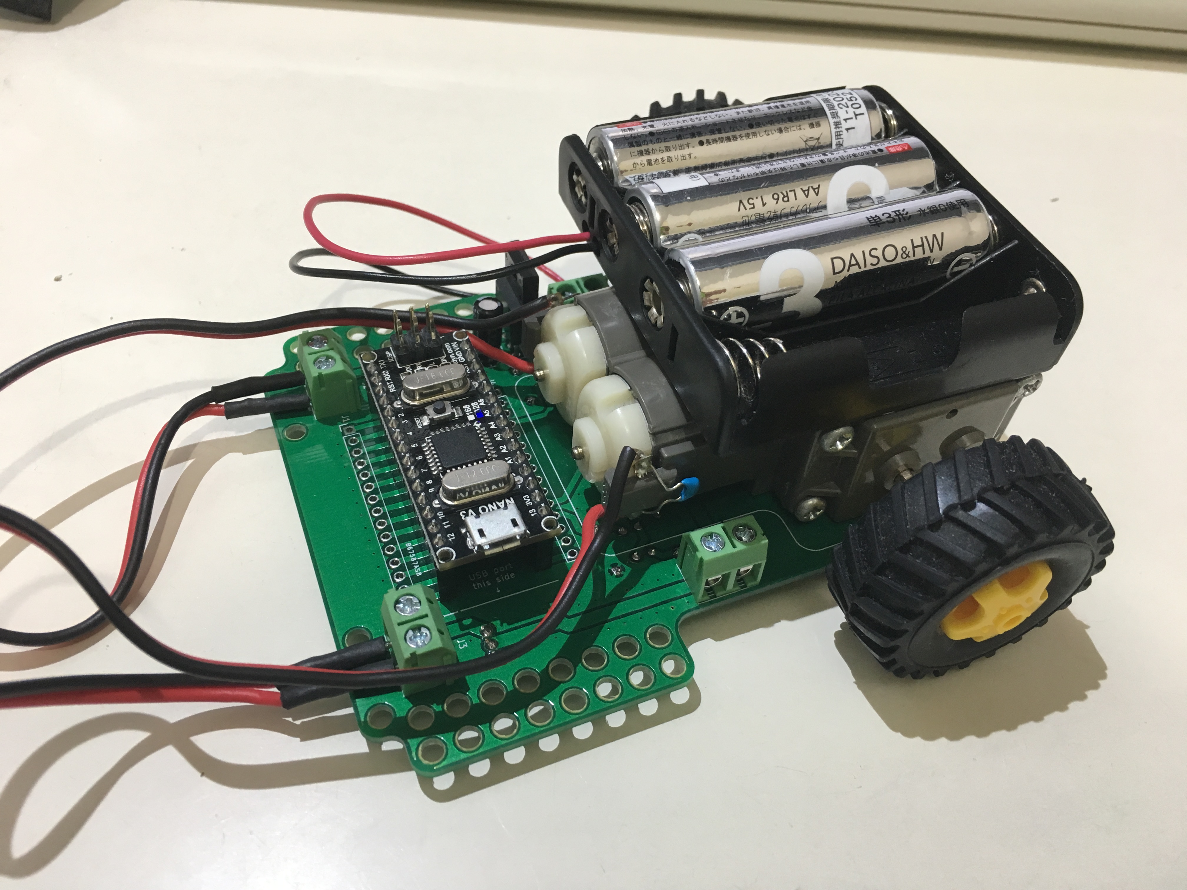
Line Tracer board for education.
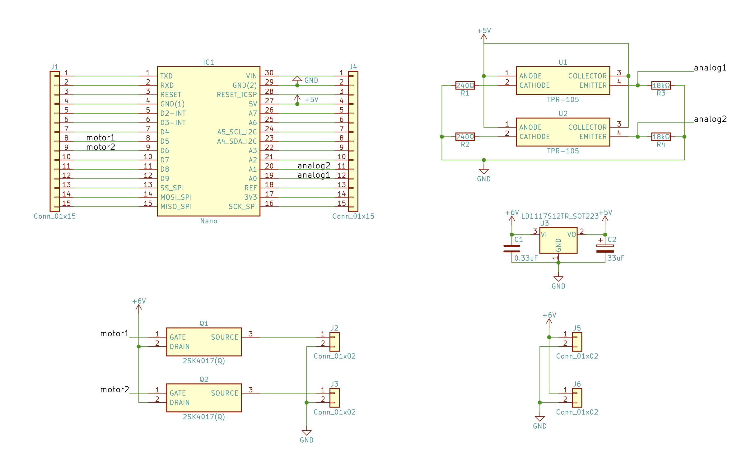
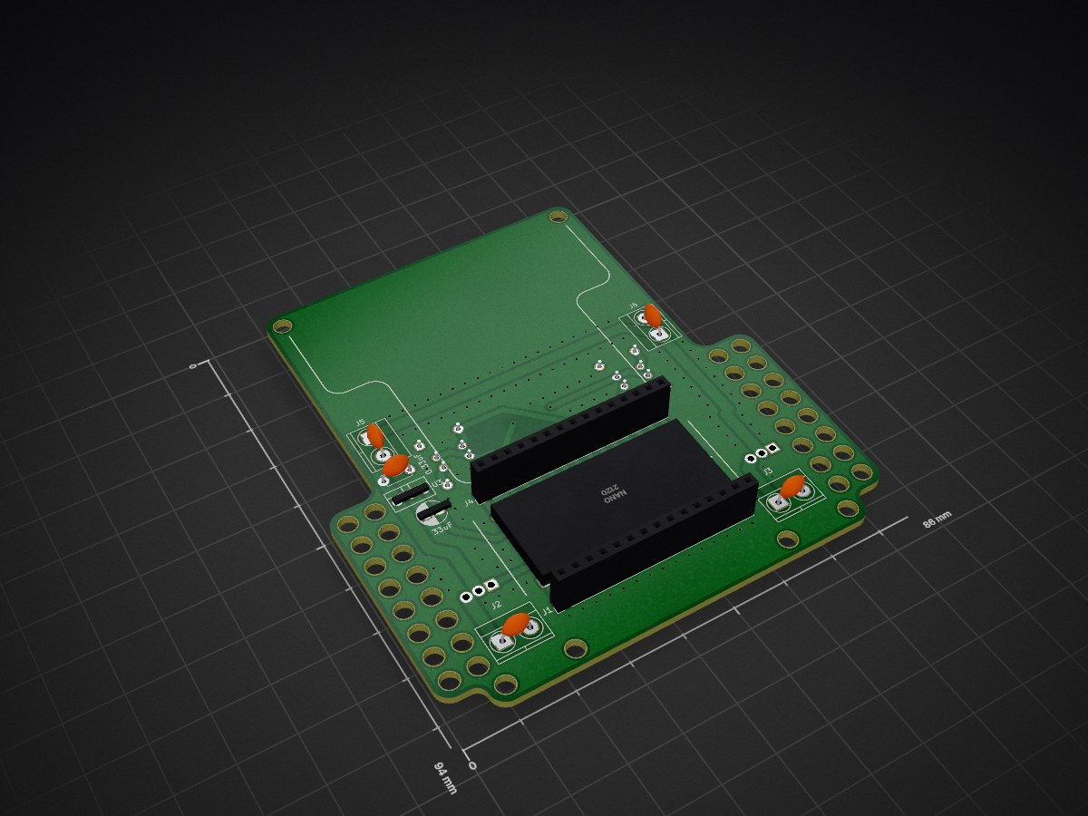
Linetrace main is an open-source printed circuit board by KeioRoboticsAssociation, from the KeioRoboticsAssociation/LineTracer repository on GitHub. It is a 2-layer board of 86 × 94 mm with 153 parts on 35 nets, routed with 99 tracks and 143 vias.
It is built around the 2SK4017(Q). Its parts include 6 connectors, 4 ICs and 2 transistors.
| Qty | Value | Footprint | References |
|---|---|---|---|
| 134 | MountingHole_3.2mm_M3 | Mounting_Holes:MountingHole_3.2mm_M3 | , , , , , , , , , , , , , , , +118 |
| 4 | Conn_01x02 | mylib2:TerminalBlock_small | J2, J3, J5, J6 |
| 2 | 18kΩ | Resistors_THT:R_Axial_DIN0207_L6.3mm_D2.5mm_P7.62mm_Horizontal | 18kΩ, 18kΩ |
| 2 | 240Ω | Resistors_THT:R_Axial_DIN0207_L6.3mm_D2.5mm_P7.62mm_Horizontal | 240Ω, 240Ω |
| 2 | 2SK4017(Q) | 2SK4017(Q):TO230P250X650X900-3P | Q1, Q2 |
| 2 | Conn_01x15 | Pin_Headers:Pin_Header_Straight_1x15_Pitch2.54mm | J1, J4 |
| 2 | TPR-105 | mylib2:TPR-105_new | U1, U2 |
| 1 | 0.33uF | Capacitors_THT:C_Disc_D4.7mm_W2.5mm_P5.00mm | 0.33uF |
| 1 | 33uF | Capacitors_THT:CP_Radial_D5.0mm_P2.50mm | 33uF |
| 1 | LD1117S12TR_SOT223 | mylib:OldSowjetaera_Transistor_Type-I_SmallPads | U3 |
| 1 | LOGO | mylib2:KRA | G*** |
| 1 | Nano | Nano:DIP1524W102P254L4318H762Q30N | IC1 |

Dudestin/tinyEtherDeveloper
Inexpensive FPGA board-based Ethernet evaluation board project. Consists mostly of DIP components and uses Tang PriMER. It can be built for about $50.


noritama-lab/esp32io-hw
ESP32 ベースの I/O ボードのハードウェア設計をまとめたリポジトリです。 / Hardware designs for an ESP32‑based PLC‑compatible I/O board.


0kam/ShutterClock
Low-power BLE interval timer for fixed-point Nikon DSLR cameras (XIAO nRF52840, Zephyr, Web Bluetooth)

0kam/SnowGauge
Low-cost, low-power snow depth logger for remote subalpine monitoring (NIR laser ToF + XIAO nRF52840 Sense)

airpocket-soundman/chikuwa-flute-robot
学習では、あらかじめ作った 1,000 曲のセット(runs/targetbank.npz、trainresiduales.py --bank 1000 で自動作成)から毎世代 8 曲を選んで使い回します。評価用の曲は別の乱数で作るので、学習用と重なりません。セットの中身は WAV と図で確認できます:
It measures 86 × 94 mm and has 2 copper layers, 1.6 mm thick.
153 parts, built around the 2SK4017(Q). The full list of its parts is on this page, with links to each part's symbol and footprint where PCBKit's library has them.
From the KeioRoboticsAssociation/LineTracer repository on GitHub, at the commit this page was made from: the board is linetrace_main.kicad_pcb. PCBKit opens the board in the browser, with nothing to install.
Its repository states no licence, so its author keeps all rights: ask KeioRoboticsAssociation before reusing the design.