4 layers122 × 40 mm
Implant detector
KarpelesLab/ledger_implant_detector
A small hand-held tool for spotting extra conductive structures hidden inside the plastic shell of a hardware wallet (e.g. a Ledger).
65 parts

 KarpelesLab/ledger_implant_detector
A small hand-held tool for spotting extra conductive structures hidden inside the plastic shell of a hardware wallet (e.g. a Ledger).
Integrated is an open-source printed circuit board by KarpelesLab, from the KarpelesLab/ledger_implant_detector repository on GitHub. It is a 4-layer board of 200 × 216 mm with 101 parts on 77 nets, routed with 645 tracks and 575 vias.
It is built around the AD8318ACPZ-REEL7, ADF4351BCPZ and ADS1115IDGSR, with the AP2112K-3.3TRG1, OT322525MJBA4SL and U.FL-R-SMT-1(80) among its other parts. Its parts include 34 capacitors, 29 resistors, 5 ICs, 5 connectors and 4 inductors. It belongs with the RP2040 boards of this library.


⚠️ STATUS: CONCEPT — NOT YET BUILT OR VALIDATED (rev 0.1)
This hardware has not been fabricated or tested yet. The schematic, layout and detection method are a first-pass concept and will almost certainly need errata. Do not rely on this device to declare a wallet "clean" until the design has been built, characterised against known-good and known-tampered devices, and this banner has been removed.
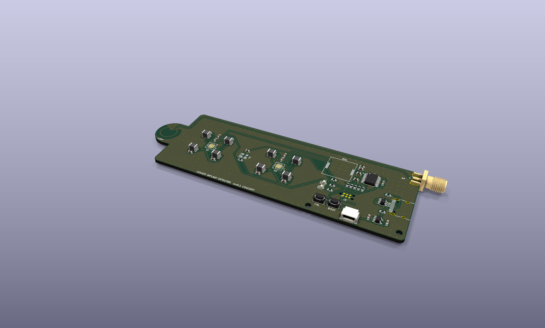
A small hand-held tool for spotting extra conductive structures hidden inside the plastic shell of a hardware wallet (e.g. a Ledger). The target threat is a supply-chain implant that adds a cellular (LTE) modem to the device: such implants need a comparatively large antenna, i.e. a sizeable area of copper that is not present in a genuine unit.
Everything is on one board, powered and programmed over a single USB-C port. No programmer or debug probe is needed (see Programming).
The tool combines two complementary methods:
Eight 14 × 14 mm copper electrodes on the underside of the head are read by two TI FDC2214 28-bit capacitance-to-digital converters (LC-resonant, EMI tolerant). Any conductor close to a plate (an antenna trace, a ground plane, a battery…) increases that plate's capacitance and lowers its resonance frequency, which the FDC2214 measures with very high resolution.
The detector does not recognise an antenna by itself: a genuine wallet also contains copper (PCB, battery, display, Bluetooth antenna, NFC coil on newer models). The method is differential:
The array covers 65 × 34 mm, enough for a Nano S Plus / Nano X in a single placement; Stax / Flex need two or more positions.
The nose of the board carries a printed 8 mm H-field loop, fed by a 50 Ω microstrip that runs back to an edge SMA connector next to the USB-C port. Plug in an inexpensive VNA (NanoVNA / LiteVNA), sweep S11 from roughly 600 MHz to 3 GHz and hover the tip over the wallet. You are looking for resonances in the LTE bands that a genuine unit does not show.
This is complementary to the capacitive method: capacitance tells you where there is extra copper, and the RF sweep hints at whether that copper is tuned like an antenna. Results are again comparative (reference unit vs. unit under test). The wallet's own ground plane, battery, Bluetooth antenna and NFC coil all produce responses of their own, and a hidden antenna's resonance shifts with its surroundings.
A later revision is meant to integrate the RF sweep so no external VNA is needed. The measurements in docs/rf_measurements.md will decide whether a magnitude-only front end is enough or phase is needed.
docs/simulation.md models the real antenna (from photos of a tampered unit) sandwiched between the shell and the Ledger's own battery. Summary so far: antenna copper that sticks out beyond the battery's outline is clearly detectable, above any plausible placement error. Copper lying entirely within the battery's outline (it is always glued between the shell and the battery) and electrically floating is not detectable capacitively. Placement (air gap) dominates the raw signal, so the wallet must be pressed flat and judged by the shape of the 8-channel signature. The RF loop over the antenna's feed area shows a narrow in-band absorption dip (~0.35 dB, at ~1.8 GHz in the model) that a plain-copper piece of the same outline does not. That feature tells an antenna apart from a battery or other metal, and is within reach of a scalar, VNA-less front end.
The first NanoVNA session on a tampered Nano X (data/rf/2026-10-18/notes.md) found a clear S21 hump at 820-850 MHz, but only with the probe right over the antenna's feed. To remove that position dependence there is now a concept RF fixture kit (slot line and open TEM cell, 80 × 80 mm test area, NanoVNA S11/S21), with JLCPCB files. See docs/fixtures.md. In simulation, both fixtures see a narrow tampering notch at every wallet placement tested.
First fixture measurements (2026-10-26, one genuine and one tampered Nano X, data/rf/2026-10-26/notes.md): the TEM cell shows a ~1 dB, ~40 MHz wide notch at 1171 MHz on the tampered unit in all 12 captures, at every placement and in both orientations. The simulation predicted -1.2 dB at 1185 MHz. 18 of 19 genuine captures stay within 0.22 dB. One genuine capture showed a similar notch at ~1230 MHz that did not repeat, cause unknown. The slot line sees the antenna's 820-860 MHz resonance only weakly (~0.15 dB) and only at 0 deg. This is promising but not yet validation: it is one unit of each kind.
A second, quite different implant (Joe Grand's tampered Nano X: a hand-wound ~6 mm wire spiral antenna and a shortened battery) is not seen by the fixtures in simulation: the coil is too small to couple to a uniform field. The capacitive array catches it clearly through the missing battery foil (1.3-3.4 pF above placement error). So always run both tests.
Two large crossed H-field loops (an induction-balance setup) were also simulated (docs/fixtures.md). Crossed vertical loops show the meander implant's 825-840 MHz resonance as a 10-13 dB narrow peak at every placement, but only 57-70 dB below the drive level, which is hard for a NanoVNA. Wallet-sized coaxial loops miss that resonance entirely. For now the TEM cell remains the practical test.
The next step is an integrated TEM cell with its own scalar sweep, an LCD, green and
red LEDs and USB-C: see docs/rev02_integrated.md. The board is generated in
hardware/integrated/ but has not been built, and it has no firmware yet.
| Top | Bottom (sensing side) |
|---|---|
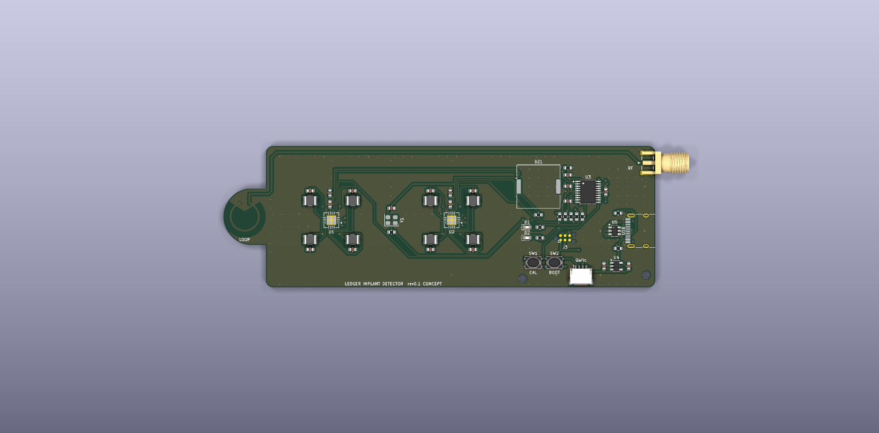 | 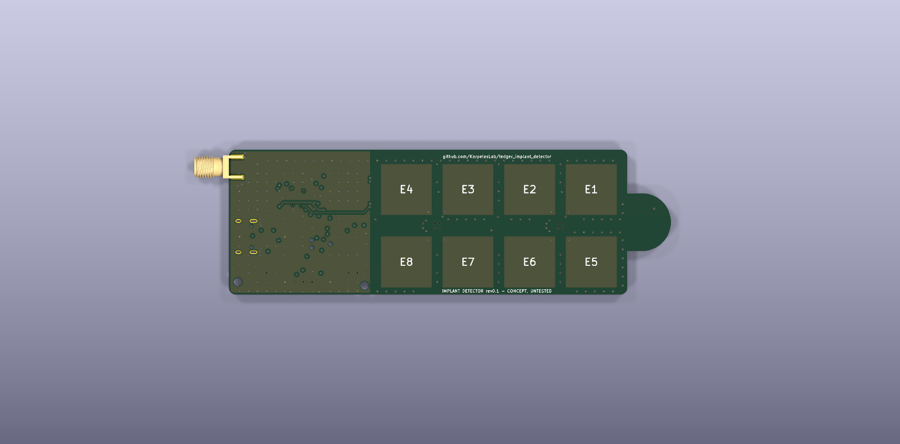 |
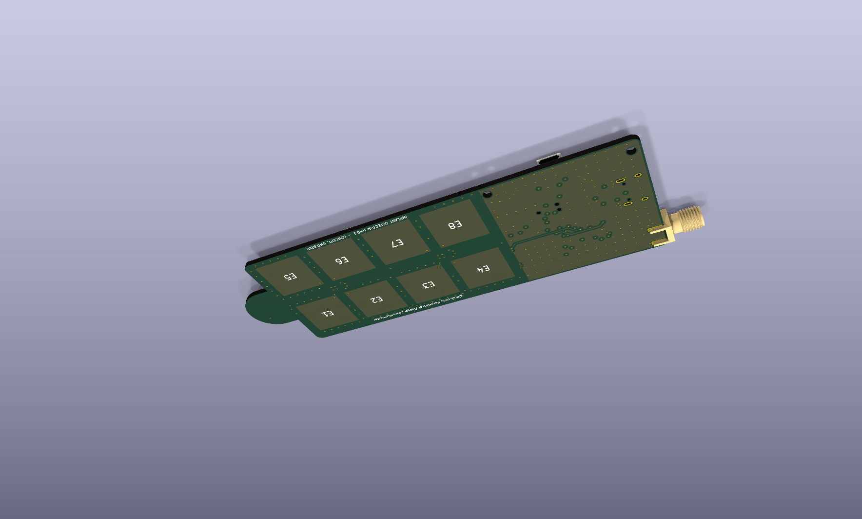
Bottom copper, seen from below (i.e. the face you put against the wallet):
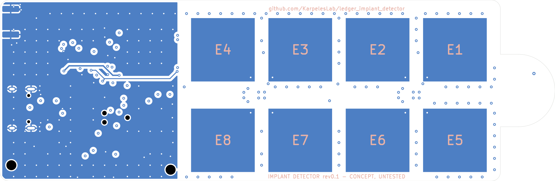
| Electrode | Converter | Channel |
|---|---|---|
| E1 / E5 / E6 / E2 | U1 (I²C 0x2A) | CH0 / CH1 / CH2 / CH3 |
| E3 / E7 / E8 / E4 | U2 (I²C 0x2B) | CH0 / CH1 / CH2 / CH3 |
Electrode numbering (E1…E4 = row nearest the RF edge, E1 nearest the nose) is also printed on the bottom silkscreen.
4 layers, 1.6 mm (JLC04161H-7628):
| Layer | Use |
|---|---|
| F.Cu | components, routing, GND pour, RF microstrip (0.35 mm ≈ 50 Ω over In1) |
| In1.Cu | solid GND: RF reference plane, and passive shield behind the electrodes so the hand holding the tool is not sensed |
| In2.Cu | routing only outside the electrode areas (keep-outs over every electrode); GND pour under the handle |
| B.Cu | the 8 electrodes (solder-mask covered); GND pour under the handle only |
Each FDC2214 sits on top of the board in the gap between its four electrodes, so the sensor feed-throughs are only a few millimetres long.
| Block | Part | Notes |
|---|---|---|
| CDC ×2 | TI FDC2214RGHR | single-ended sensors, 0x2A / 0x2B |
| Tank ×8 | 18 µH (Bourns CMH322522-180KL) ‖ 33 pF C0G 1 % | ≈ 5–6.5 MHz, values from the TI datasheet / EVM |
| Clock | 40 MHz CMOS oscillator (Abracon ASE) | shared by both FDCs |
| MCU | STM32F042F6P6 (TSSOP-20) | crystal-less USB FS, ROM USB-DFU bootloader |
| USB | USB-C (HRO TYPE-C-31-M-12), USBLC6-2SC6 ESD | 5.1 kΩ CC pull-downs (sink, 5 V only) |
| Power | AP2112K-3.3 LDO | |
| RF | printed 8 mm loop + Samtec SMA-J-P-H-ST-EM1 edge SMA | |
| UI | green + red LED, Murata PKLCS1212E piezo, CAL + BOOT buttons | |
| Expansion | JST-SH 4-pin (Qwiic / STEMMA-QT pinout) for an optional I²C OLED | |
| Debug | Tag-Connect TC2030-NL footprint (SWD), no part needed |
| Pin | Function |
|---|---|
| PF0 / PF1 | I2C1 SDA / SCL (both FDCs + Qwiic) |
| PA0 / PA1 | FDC U1 / U2 INTB (10 k pull-ups) |
| PA2 | FDC SD (shutdown, both chips; 100 k pull-down = running) |
| PA3 / PA4 | LED green / red (active high) |
| PA5 | CAL button (to GND, enable internal pull-up) |
| PA6 | piezo buzzer (TIM3_CH1 / TIM16_CH1 PWM) |
| PA11 / PA12 | USB D− / D+ (TSSOP-20 pins 17/18, set SYSCFG_CFGR1.PA11_PA12_RMP) |
| PA13 / PA14 | SWDIO / SWCLK (Tag-Connect pads) |
| BOOT0 | BOOT button to 3V3 (10 k pull-down) |
The STM32F042 has a USB-DFU bootloader in ROM, so firmware is flashed through the same USB-C port that powers the board:
dfu-util -a 0 -s 0x08000000:leave -D firmware.binSTM32CubeProgrammer (USB mode) works too. The Tag-Connect SWD footprint is only there as a recovery/debug path for people who own a probe.
To validate on the first build: that ROM DFU enumerates on the TSSOP-20 package (USB on the remapped pins 17/18), and the option-byte state of the BOOT0 pin on the delivered parts.
Starting point, from datasheet §8.2.3:
CLOCK_DIVIDERS_CHx = 0x2001 (CHx_FIN_SEL = b10, single-ended sensor; CHx_FREF_DIVIDER = 1)CONFIG.REF_CLK_SRC = 1DRIVE_CURRENT_CHx so the tank amplitude is 1.2–1.8 Vpk (start around IDRIVE = 15)MUX_CONFIG.AUTOSCAN_EN = 1, RR_SEQUENCE = b10, deglitch 10 MHzhardware/
lib/ project symbols + footprints (FDC2214, electrode, near-field loop)
detector/ KiCad 10 project (schematic + 4-layer PCB)
fab/ gerbers + drill (zip), BOM, JLC BOM/CPL, schematic PDF
docs/img/ renders
tools/ Python generators used to produce the KiCad files and outputsThe KiCad files were generated by the scripts in tools/ so the first
revision is reviewable as code. They are ordinary KiCad projects, though: once
you edit them by hand in KiCad, treat the KiCad files as the source of truth.
Regenerating needs KiCad 10 (its Python pcbnew module and kicad-cli). Routing also
needs Java 17+ and Freerouting 1.9.0.
1.9 routes this board completely; 2.x did noticeably worse on it. 1.9 needs an X
display, and Xvfb works.
python3 tools/gen_lib.py              # project library
python3 tools/gen_detector_sch.py     # schematic
Xvfb :97 & export DISPLAY=:97
FREEROUTING_JAR=/path/to/freerouting-1.9.0.jar FREEROUTING_PASSES=100 \
    python3 tools/gen_detector_pcb.py # placement, pre-routing, autoroute, pours, stitching
python3 tools/make_outputs.py         # gerbers/drill/BOM/CPL/PDF + renders
The PCB generator places everything, then hand-routes these parts deterministically: the RF microstrip, the converters' digital escapes, the north-side power/control escapes, the tank for the electrode diagonally opposite each converter's analog pins, and a small bus to the handle. It fans every GND pad out to the In1 plane and lets Freerouting do the rest. GND is not autorouted: it comes from pours on F.Cu / In1 (and In2 / B.Cu under the handle) plus stitching vias.
Current check status (hardware/detector/fab/*_report.txt): ERC 0 violations;
DRC 0 errors, 0 unconnected, schematic parity OK. The remaining warnings are two
"silkscreen clipped by board edge" from the stock USB-C footprint and three
single-spoke thermal reliefs on pads that also have a direct via to the GND plane.
hardware/detector/fab/ contains everything for a 4-layer PCB + assembly
order:
implant_detector_gerbers.zip: select 4 layers, 1.6 mm, and the
JLC04161H-7628 stack-up (the 0.35 mm RF line is 50 Ω only on that stack-up).
Minimum features: 0.15 mm track/space, 0.3 mm drill / 0.6 mm via, so no
advanced-capability options are needed.bom_jlc.csv + cpl_jlc.csv (origin = bottom-left corner of the board).
MPNs are given; only the USB-C connector has a pre-filled LCSC number, so
let the assembler match the rest by MPN and check the rotations in the
assembly preview, especially U1/U2/U3, the LEDs and J1.schematic.pdf for reference.tools/analyze_s1p.py.Not yet chosen.
| Qty | Value | Footprint | References |
|---|---|---|---|
| 13 | 100n | Capacitor_SMD:C_0603_1608Metric | C10, C11, C12, C14, C15, C17, C18, C20, C24, C26, C30, C31, C34 |
| 10 | MountingHole_3.2mm_M3 | MountingHole:MountingHole_3.2mm_M3 | H1, H2, H3, H4, H5, H6, H7, H8, H9, H10 |
| 8 | 100p | Capacitor_SMD:C_0603_1608Metric | C3, C4, C5, C6, C16, C19, C25, C27 |
| 7 | 49.9 | Resistor_SMD:R_0603_1608Metric | R5, R6, R7, R8, R9, R10, R24 |
| 4 | 0 | Resistor_SMD:R_0603_1608Metric | L1, R1, R20, R26 |
| 4 | 600R | Inductor_SMD:L_0603_1608Metric | FB1, FB2, FB3, FB4 |
| 3 | 330 | Resistor_SMD:R_0603_1608Metric | R13, R36, R37 |
| 3 | DNP | Capacitor_SMD:C_0603_1608Metric | C1, C2, C13 |
| 2 | 100 | Resistor_SMD:R_0603_1608Metric | R2, R4 |
| 2 | 100k | Resistor_SMD:R_0603_1608Metric | R29, R30 |
| 2 | 10n | Capacitor_SMD:C_0603_1608Metric | C28, C29 |
| 2 | 150 | Resistor_SMD:R_0603_1608Metric | R21, R23 |
| 2 | 1k | Resistor_SMD:R_0603_1608Metric | R27, R28 |
| 2 | 1n | Capacitor_SMD:C_0603_1608Metric | C21, C22 |
| 2 | 4.7k | Resistor_SMD:R_0603_1608Metric | R32, R33 |
| 2 | DNP | Connector_Coaxial:SMA_Samtec_SMA-J-P-H-ST-EM1_EdgeMount | J1, J2 |
| 1 | +3V3A | TestPoint:TestPoint_Pad_D1.5mm | TP4 |
| 1 | +5VA | TestPoint:TestPoint_Pad_D1.5mm | TP5 |
| 1 | 1.5n | Capacitor_SMD:C_0603_1608Metric | C7 |
| 1 | 10k | Resistor_SMD:R_0603_1608Metric | R34 |
| 1 | 10u | Capacitor_SMD:C_0805_2012Metric | C33 |
| 1 | 15n | Capacitor_SMD:C_0603_1608Metric | C8 |
| 1 | 220p | Capacitor_SMD:C_0603_1608Metric | C23 |
| 1 | 25 MHz | Oscillator:Oscillator_SMD_Abracon_ASE-4Pin_3.2x2.5mm | Y1 |
| 1 | 33 | Resistor_SMD:R_0603_1608Metric | R14 |
| 1 | 39 | Resistor_SMD:R_0603_1608Metric | R22 |
| 1 | 4.7u | Capacitor_SMD:C_0805_2012Metric | C32 |
| 1 | 47 | Resistor_SMD:R_0603_1608Metric | R35 |
| 1 | 499 | Resistor_SMD:R_0603_1608Metric | R25 |
| 1 | 5.1k | Resistor_SMD:R_0603_1608Metric | R11 |
| 1 | 510 | Resistor_SMD:R_0603_1608Metric | R12 |
| 1 | 68 | Resistor_SMD:R_0603_1608Metric | R3 |
| 1 | 680p | Capacitor_SMD:C_0603_1608Metric | C9 |
| 1 | AD8318 | Package_CSP:Analog_LFCSP-16-1EP_4x4mm_P0.65mm_EP2.35x2.35mm | U3 |
| 1 | ADC_3 | TestPoint:TestPoint_Pad_D1.5mm | TP6 |
| 1 | ADF4351 | Package_DFN_QFN:QFN-32-1EP_5x5mm_P0.5mm_EP3.45x3.45mm | U2 |
| 1 | ADS1115 | Package_SO:TSSOP-10_3x3mm_P0.5mm | U4 |
| 1 | AP2112K-3.3 | Package_TO_SOT_SMD:SOT-23-5 | U5 |
| 1 | DET_OUT | TestPoint:TestPoint_Pad_D1.5mm | TP1 |
| 1 | DNP | Connector_PinHeader_2.54mm:PinHeader_1x12_P2.54mm_Vertical | J4 |
| 1 | DNP | Resistor_SMD:R_0603_1608Metric | R31 |
| 1 | LCD 2.0in ST7789 | Connector_PinHeader_2.54mm:PinHeader_1x08_P2.54mm_Vertical | J3 |
| 1 | Pico 2 | Module:RaspberryPi_Pico_Common_THT | U1 |
| 1 | SYN_MUX | TestPoint:TestPoint_Pad_D1.5mm | TP3 |
| 1 | SYN_VT | TestPoint:TestPoint_Pad_D1.5mm | TP2 |
| 1 | Start | Button_Switch_THT:SW_PUSH_6mm | SW1 |
| 1 | U.FL | Connector_Coaxial:U.FL_Hirose_U.FL-R-SMT-1_Vertical | J5 |
| 1 | green | LED_THT:LED_D5.0mm | D1 |
| 1 | red | LED_THT:LED_D5.0mm | D2 |
KarpelesLab/ledger_implant_detector
A small hand-held tool for spotting extra conductive structures hidden inside the plastic shell of a hardware wallet (e.g. a Ledger).

VABISMO/QSSC
Quantum Solid State Chip - NV DIAMOND . Spin Defect Simulator and hardware controller with Qiskit backend (WIP)


joshitha-c/rf_detector
A portable, custom-built RF signal scanner and power detector designed for knowing wireless signals, measuring signal strength and can be used to be safe.


gallicchio/AMOD-and-RFMOD
The tutorial's 2x12 adapter (/mudd/133electronics/icepi-zero-dac-adc/adapterboard/) with a 2 x 6 right-angle Pmod socket on a 15 mm extension of its right-hand end, so an Icepi Zero can drive AMOD-A's and RF-MOD's Pmod…

Galacs/esp32s3-poc-devboard
ESP32-S3 based PoC board made to test step-down power supply design, 24v level shifter, crystal circuits and RF circuit

Jotrorox/minicontrol
RP2354A + 868 MHz LoRa (Ai-Thinker Ra-01SH) USB-C controller board, designed in KiCad 10.

It measures 200 × 216 mm and has 4 copper layers, 1.6 mm thick.
101 parts, built around the AD8318ACPZ-REEL7, ADF4351BCPZ, ADS1115IDGSR and AP2112K-3.3TRG1. The full list of its parts is on this page, with links to each part's symbol and footprint where PCBKit's library has them.
From the KarpelesLab/ledger_implant_detector repository on GitHub, at the commit this page was made from: the board is hardware/integrated/integrated.kicad_pcb and its schematic hardware/detector/implant_detector.kicad_sch. PCBKit opens the board in the browser, with nothing to install.
Its repository states no licence, so its author keeps all rights: ask KarpelesLab before reusing the design.