
4 layers234 × 84 mm
Main panel
google/mozc-devices
Circuit diagrams and firmware source code for Gboard DIY keyboards
234 parts3kApache-2.0

 KaiPereira/MIDI-Keypad11
Learn PCB design by creating your own custom MIDI keypad with switches, sliders, rotary encoders, neopixels and capacitive touch!
MIDI Keypad is an open-source printed circuit board by KaiPereira, from the KaiPereira/MIDI-Keypad repository on GitHub. It is a 2-layer board of 97 × 95 mm with 15 parts on 23 nets, routed with 156 tracks and 2 vias.
It is built around the SK6812MINI-E. Its parts include 4 switches, 3 diodes, 1 IC and 1 connector. It belongs with the keyboards and input and audio and music boards and the ESP32 boards of this library.
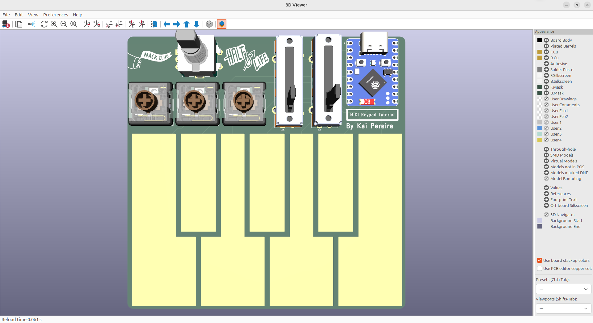
Ever wanted to cook up and mix your own beats while simultaneously learning PCB design? Well look no further because your local Kai is about to show you how to make your own custom MIDI keypad completely from scratch.
Now this is YOUR MIDI device, so please use this tutorial as a loose guide and come up with your own custom layout and features to make it awesome; go crazy!!
We'll be using these core components, and you should use any amount and combination of them for your design:
And then your actual MIDI keys will use capacitive touch which just uses exposed copper on the PCB which uses the electrical field from your body to detect presses!
We'll be using KiCad (which you'll need to install) for your PCB design, if you're not familiar with it, don't worry, because this tutorial is totally beginner friendly!
KiCad has tens of thousands of parts for you to use in the editor, but they're still missing a couple which we'll need to install. So head on over to the library I've made, which includes instructions on downloading these parts we're missing!
Once you've installed the library, we can get right into creating your schematic! The schematic shows how the components on your PCB will be wired, but it doesn't physically place them on your PCB, which we do in another step!
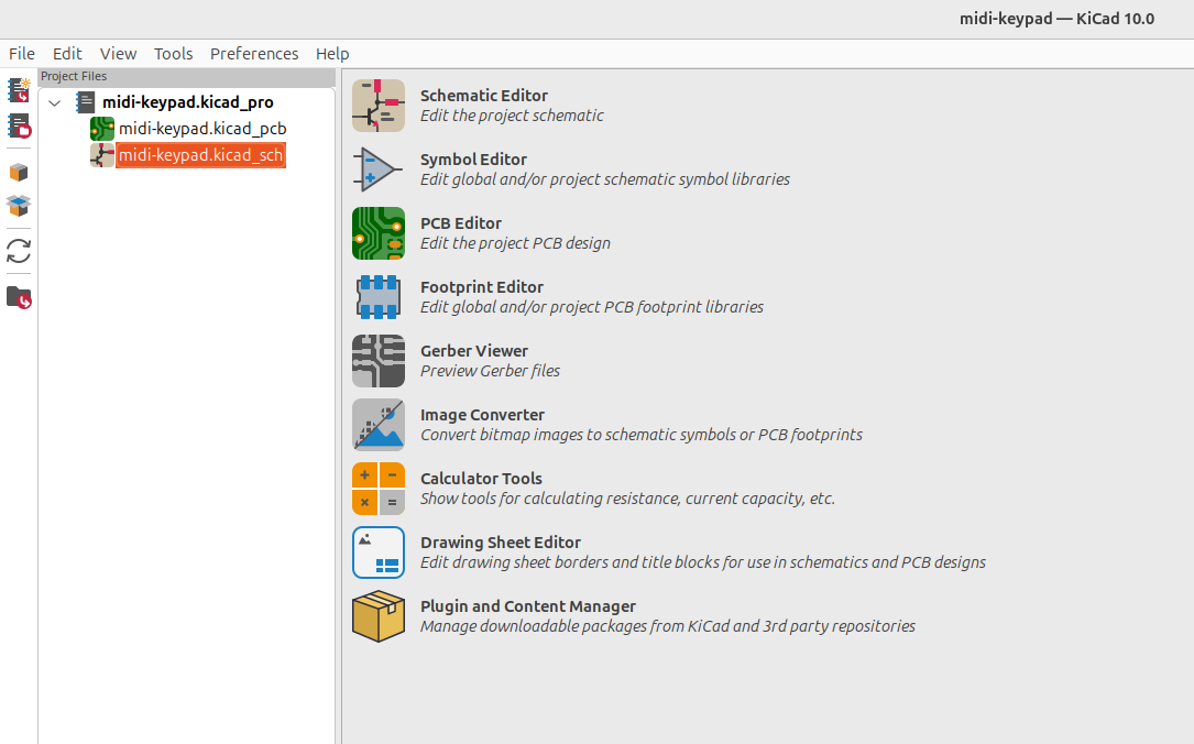
So first launch KiCad and then go "file -> new project" and use the default template and call it whatever you want! Double click on this .kicad_sch file and it'll open up the schematic editor:
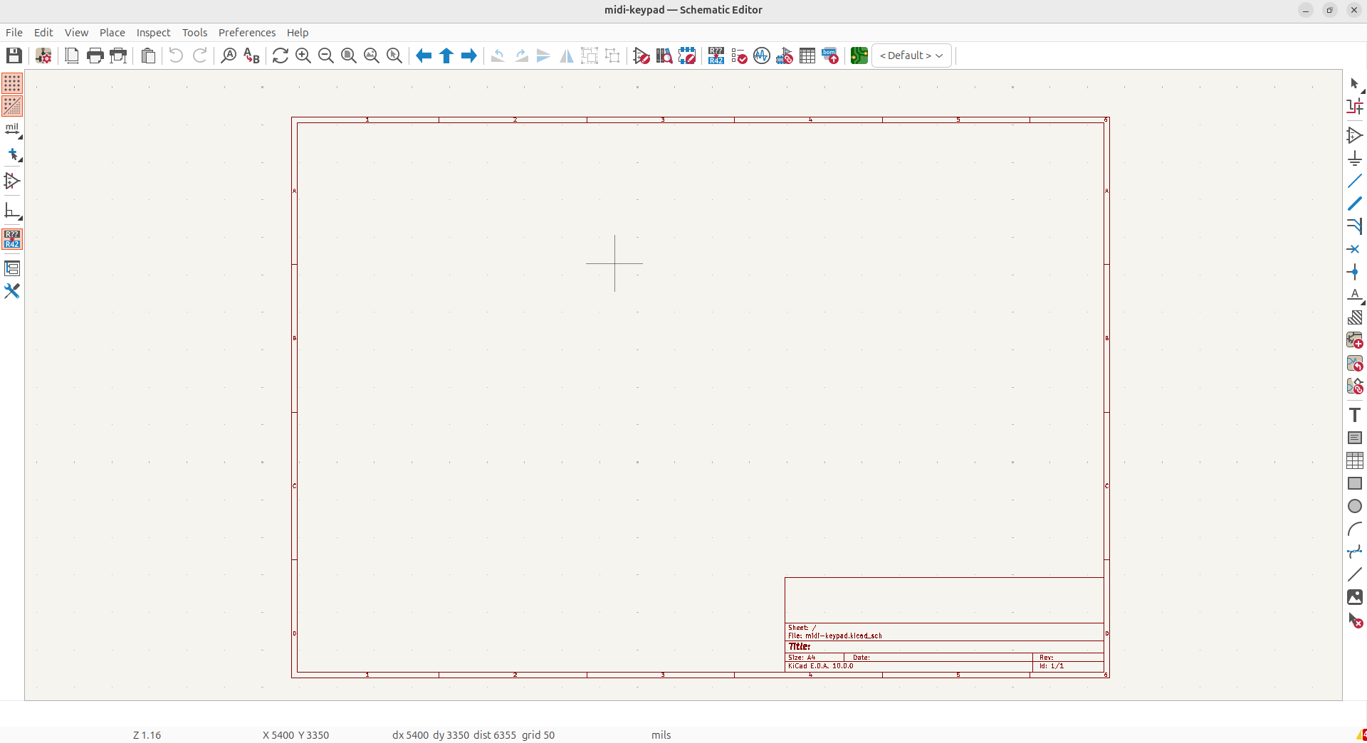
There's a couple important keybinds to keep in mind when designing PCBs:
The first thing we're going to add into our schematic, is our MCU or microcontroller. You have 2 options for microcontrollers:
Add in your chosen MCU in the symbol library using that "a" keybind we talked about:
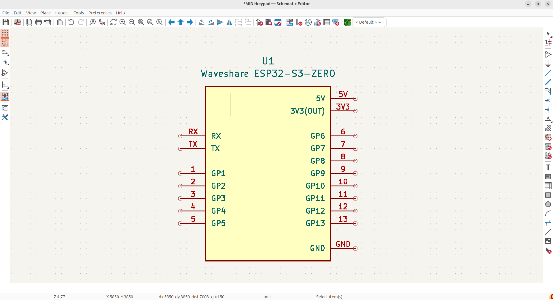
Next, we're going to wire up our power pins, because we'll be using these quite a lot in other spots on our schematic. These are called power labels and you can just find them in the symbol library:
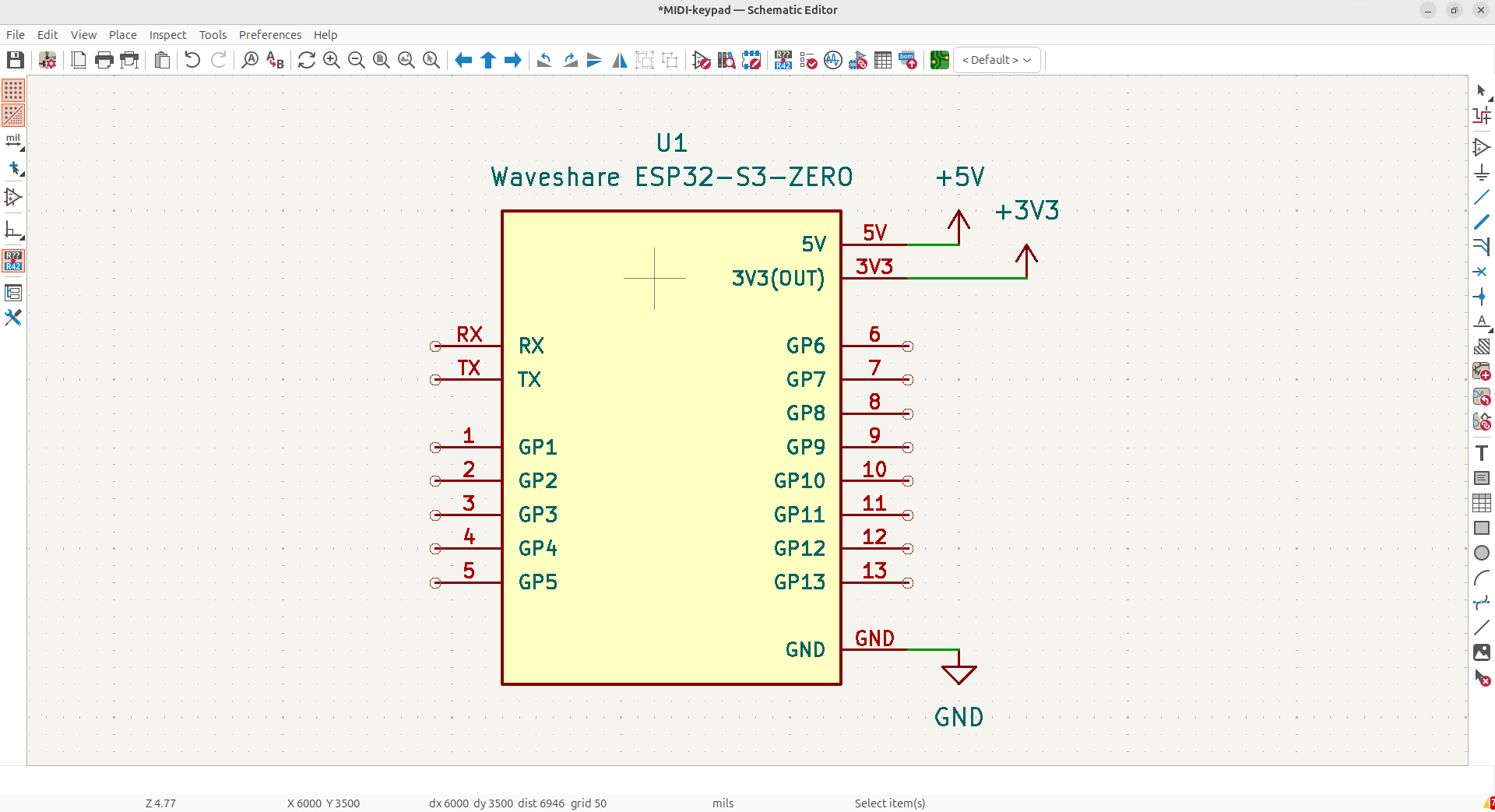
Your voltage labels should always point upwards, and your ground labels should always point downwards because once you make more complicated PCBs, it makes it really easy to read your schematics. You should also never have overlapping wires or text in your schematics, that again makes it hard to read!
Next you have the option of adding your own components for your own customizable MIDI keypad! I'll show you how to wire a couple of these components, and please make your own combination of them, you have total creative freedom:
On our MIDI keypad, we can add capacitive touch keys. These use the electrical fields generated by your body to detect if they're being touched and look awesome on your PCB!
To wire it, we'll use pin headers to represent each of our keys, so a 01x07 pin headers for 7 keys for example:
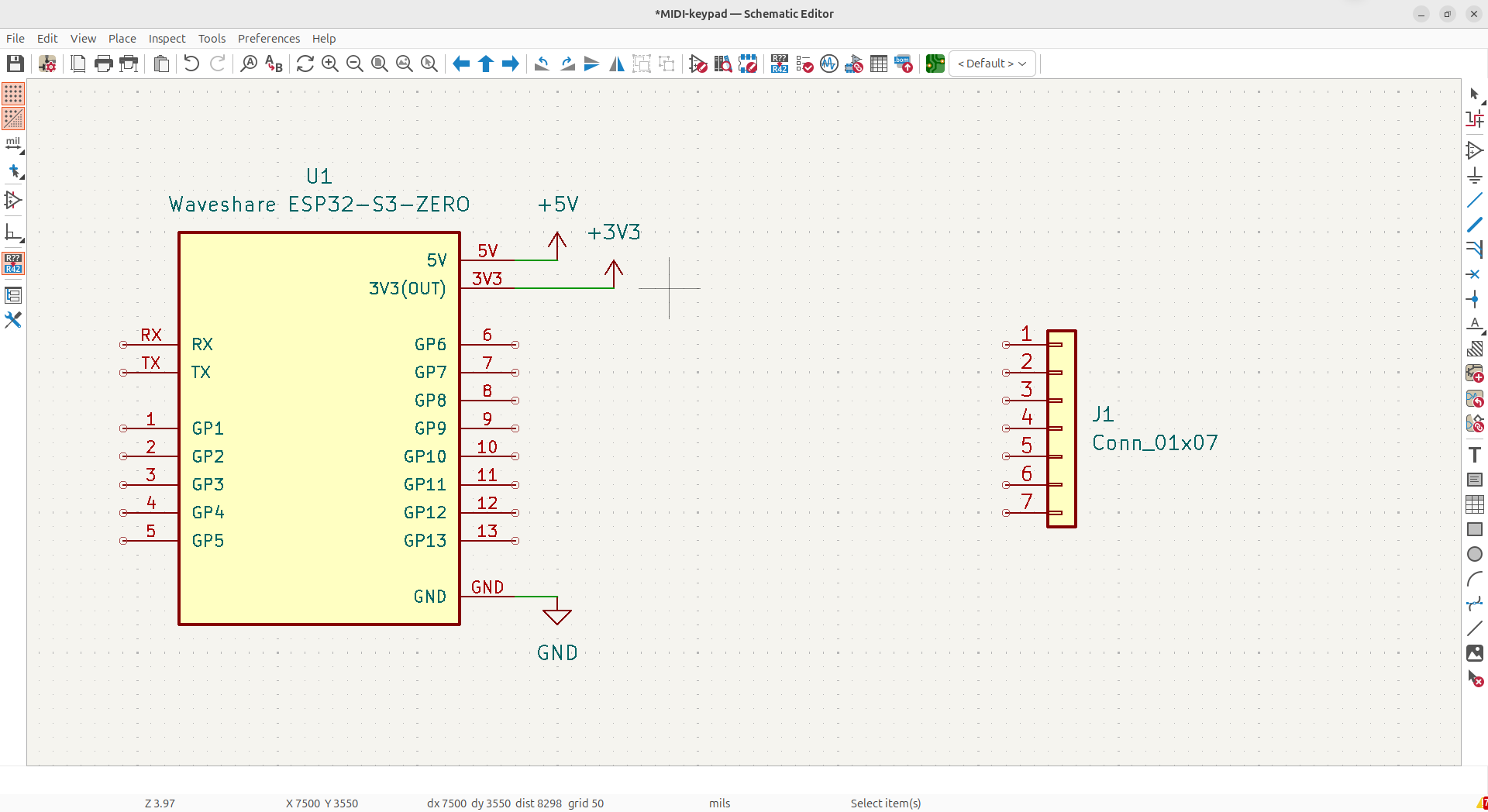
All the GPIOs except RX/TX on our Waveshare ESP32-S3-Zero can be used for capacitive touch, but only a couple on the XIAO ESP32-S3 can be used so check the pinout for that MCU.
We'll use net labels to wire these together, so tap "l" and add them in:
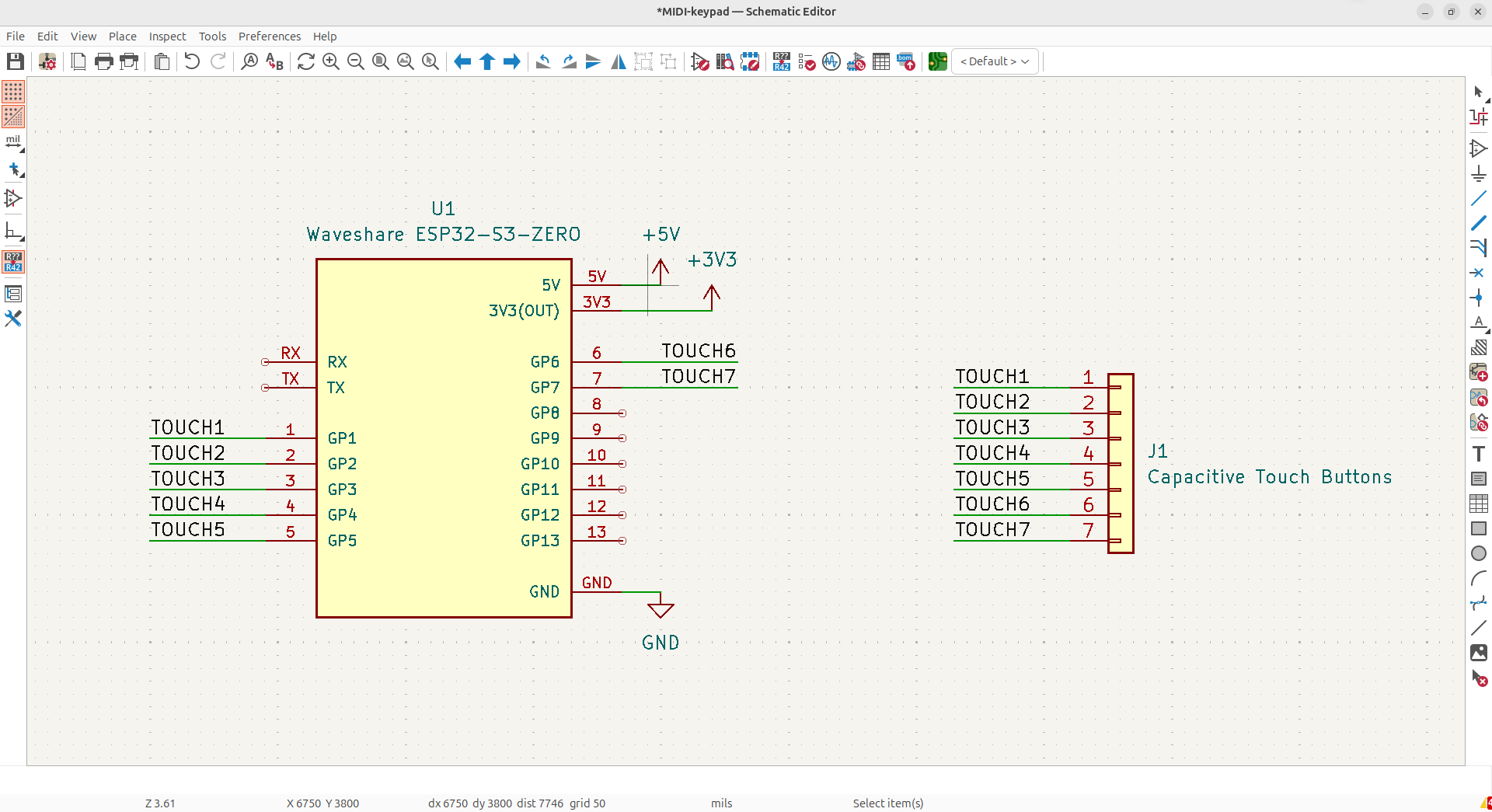
Always add nice wires underneath your net labels so they're easy to read.
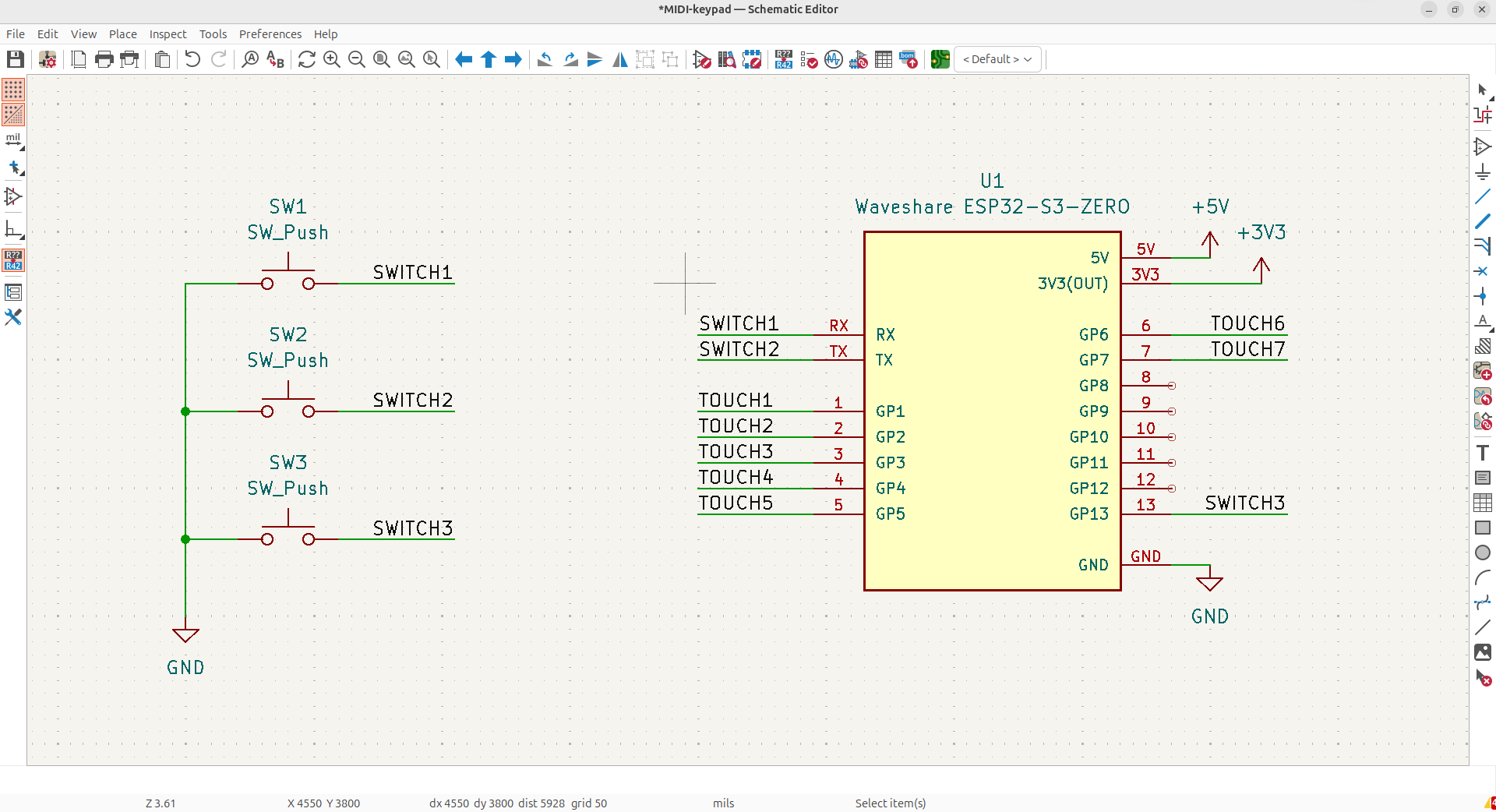
If you want to make part of your MIDI keypad have nice keyboard switches, we can easily add some in! You can just wire the switches to ground and if you want even more switches, you should look into wiring them as a matrix instead which needs some diodes but lets you have TONS of keys by using up less GPIOs.
You would want to get some nice keycaps for your switches.
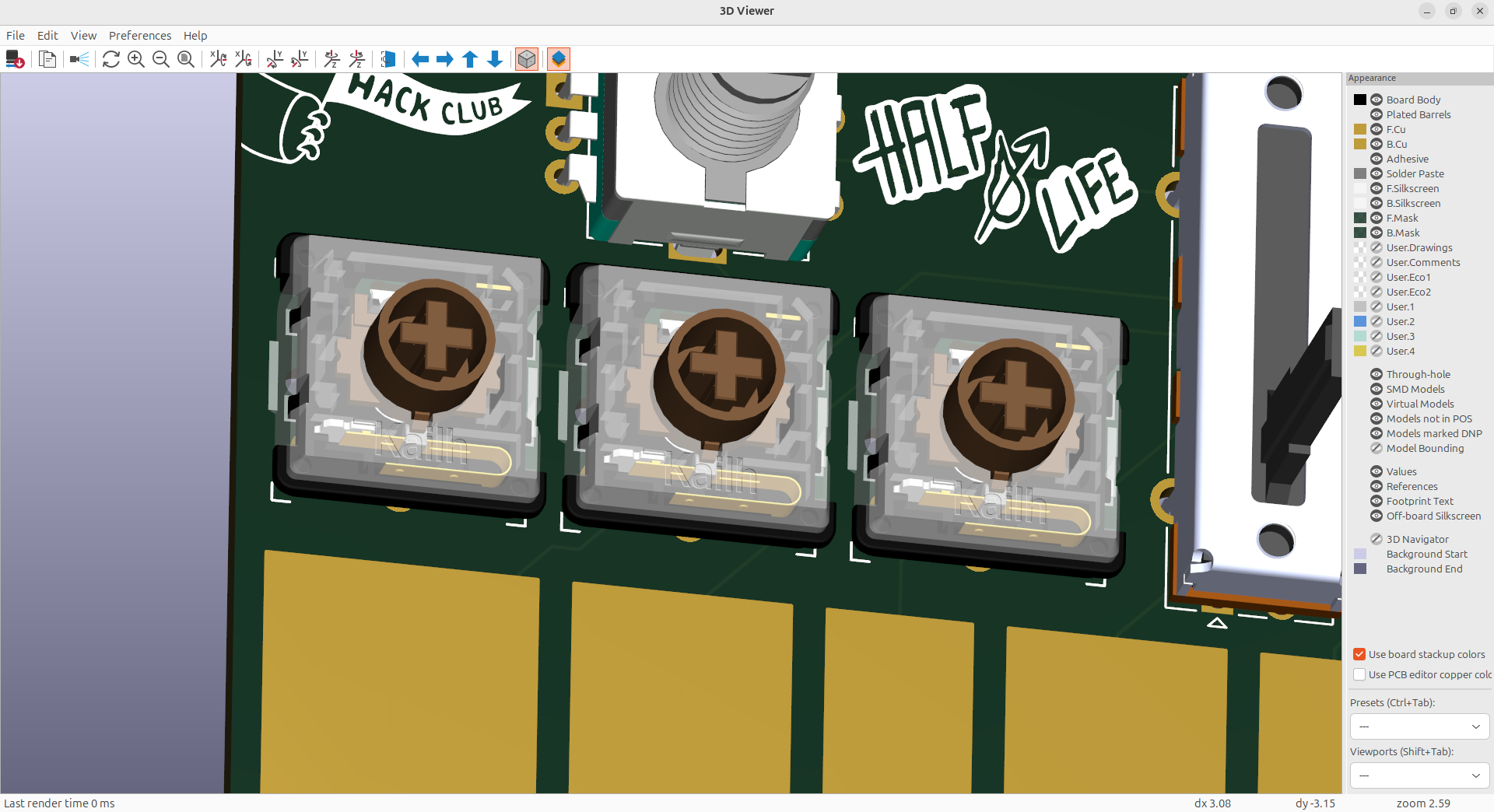
Note that RX and TX on the Waveshare MCU can be reprogrammed in your firmware to just be normal GPIO pins so they're fine to use for your switches and any other component except the capacitive touch keys which need special IOs.
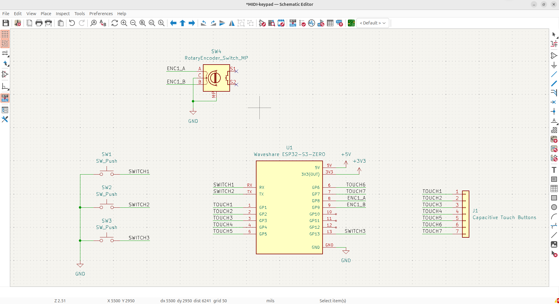
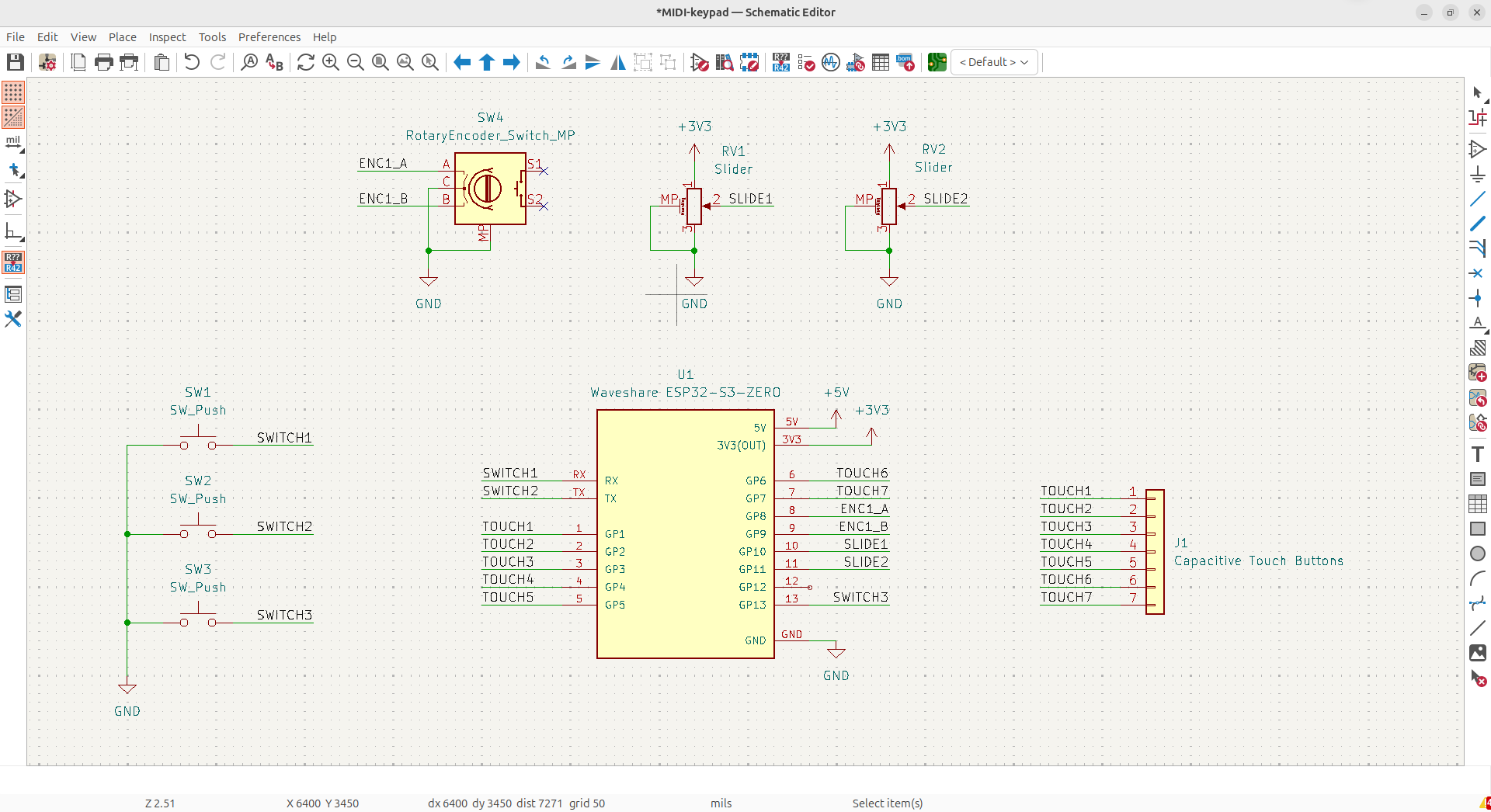
The EC11 rotary encoder has both an encoder and a switch if you want to wire it so you can also press it down. I'm only using the encoder part because I don't have much IO left and want to add some more stuff.
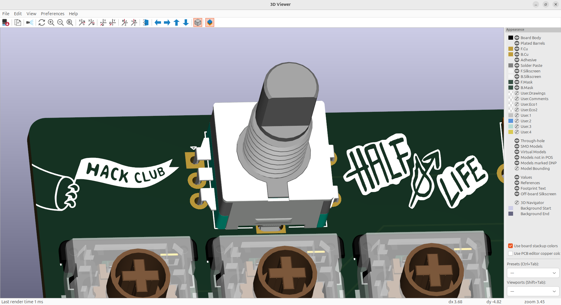
It's pretty easy to wire, it's just 2 IO pins for each direction of the pin and then a ground connection, and you can wire the switch looking part of the symbol like a normal switch or part of a matrix.
The Bourns slide potentiometer is a large slider you can add to your PCB. You can just wire pins 1 and 3 to ground and +3V3 respectively, and then wire pin 2 to an analog IO to detect its state and then the mounting pins can just be grounded.
Adding the slide potentiometer will probably increase the cost of your project a fair amount because you can't source it on Aliexpress, but you might be able to find an alternative or something.
Your slider needs to be wired up to an analog capable pin on your MCU, so check the pinouts on your MCU again and make sure the pin is ADC capable
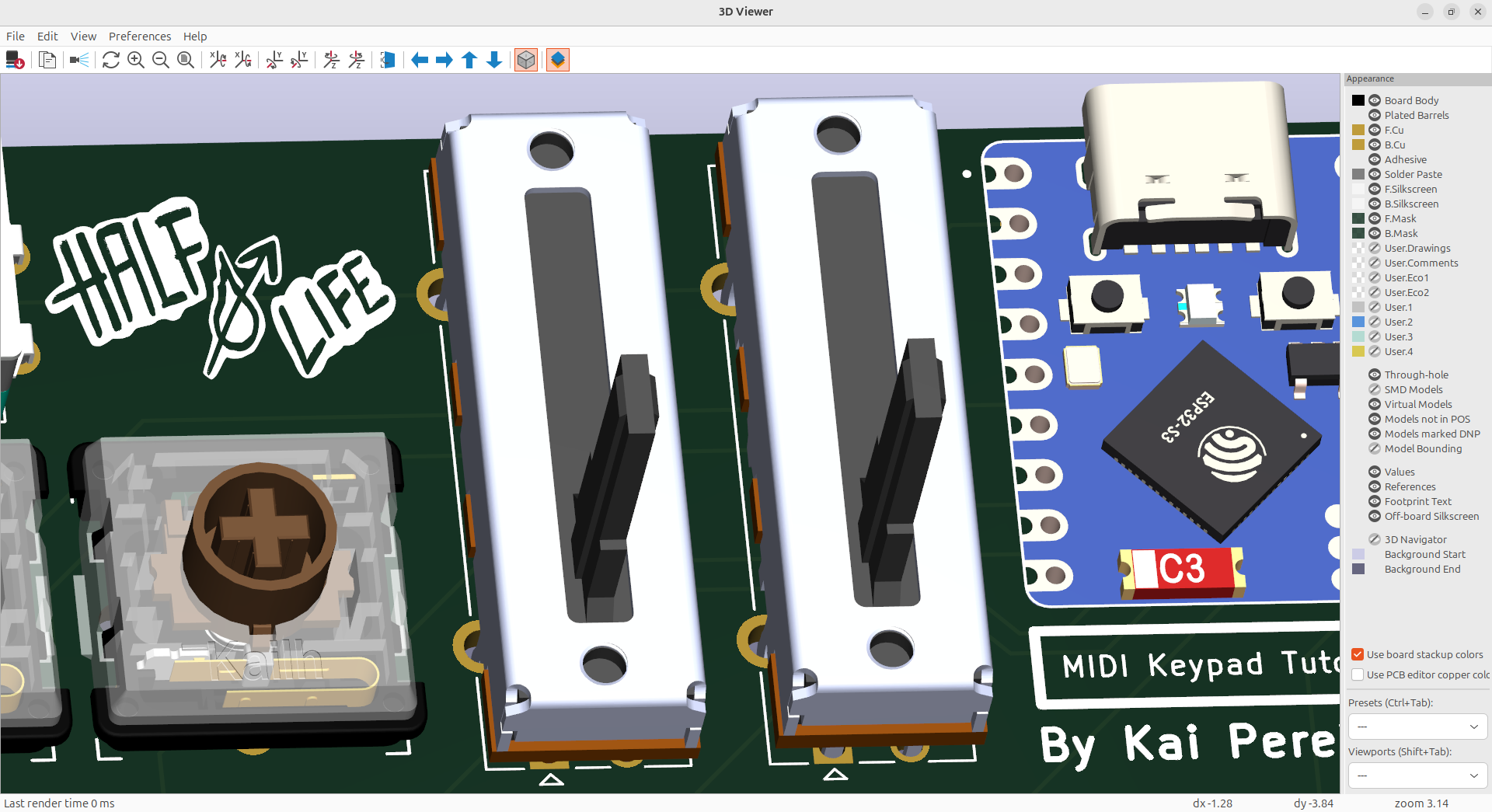
You'll want to use the "R_Potentiometer_MountingPin" symbol for this, and I've renamed my symbols here to make it more obvious what they're actually being used for.
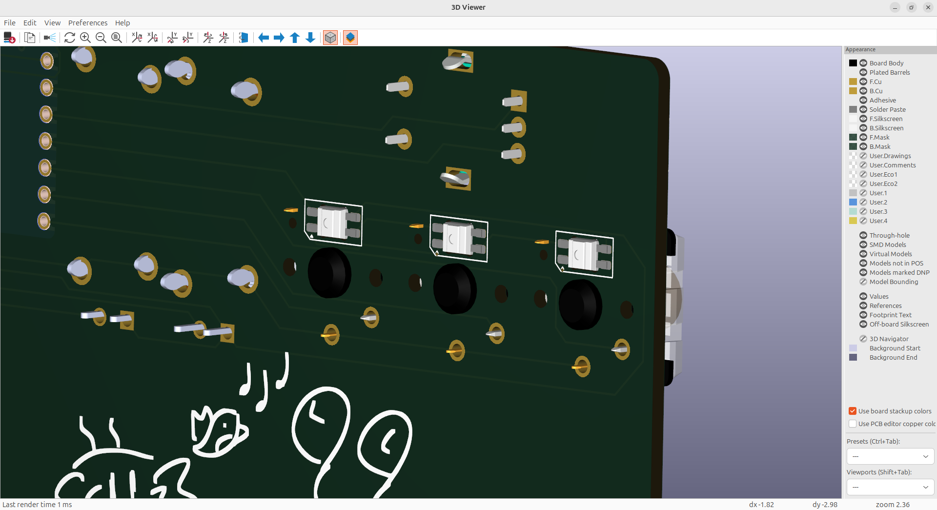
The SK6812MINI-E neopixels let you add RGB lighting to your keypad. Just wire up the power and ground pins, and then you can chain them together like so. When programming these neopixels, you'll be able to program them as the chain and can control each individually with just that singular pin.
These mount on the backside of your PCB and have a hole through the PCB so they can shine through the board
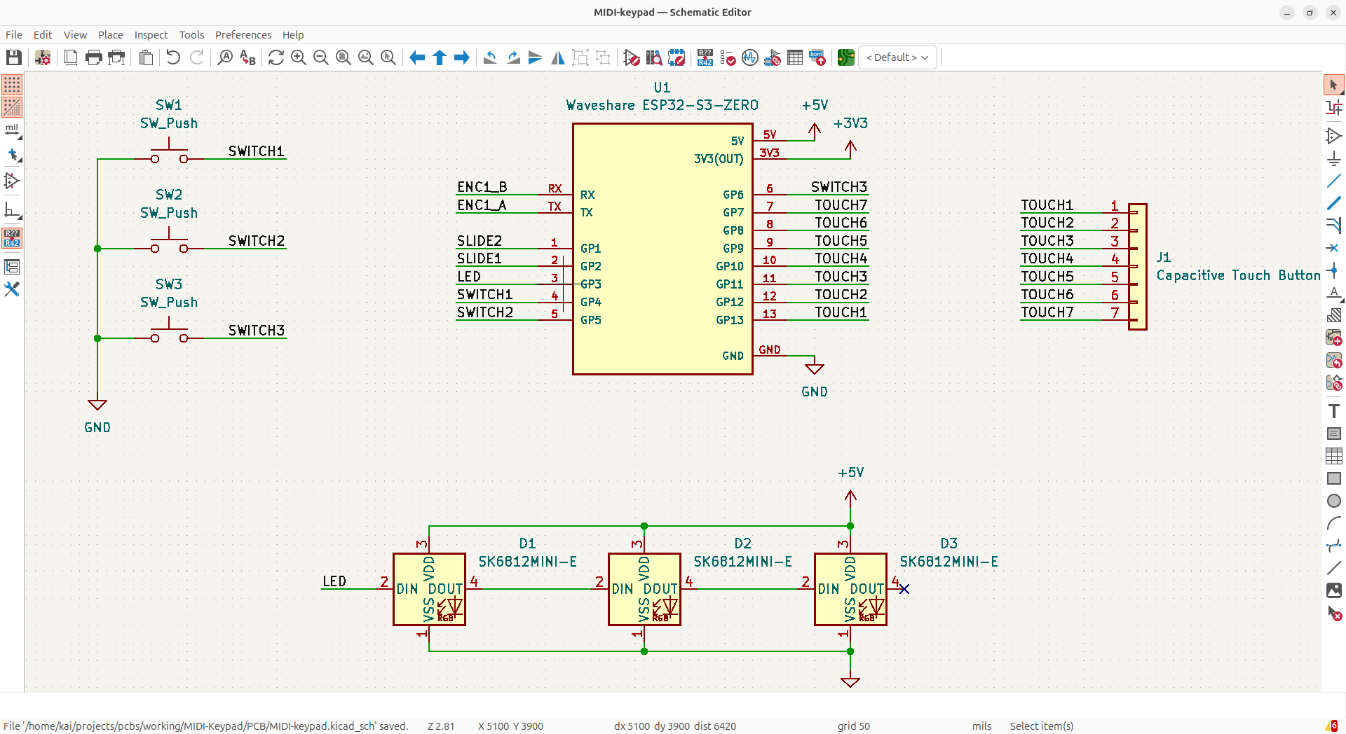
Now that we've finished our schematic, which shows the electrical connections between components, we need to assign the footprints which are the actual physical representations of the component on your PCB.
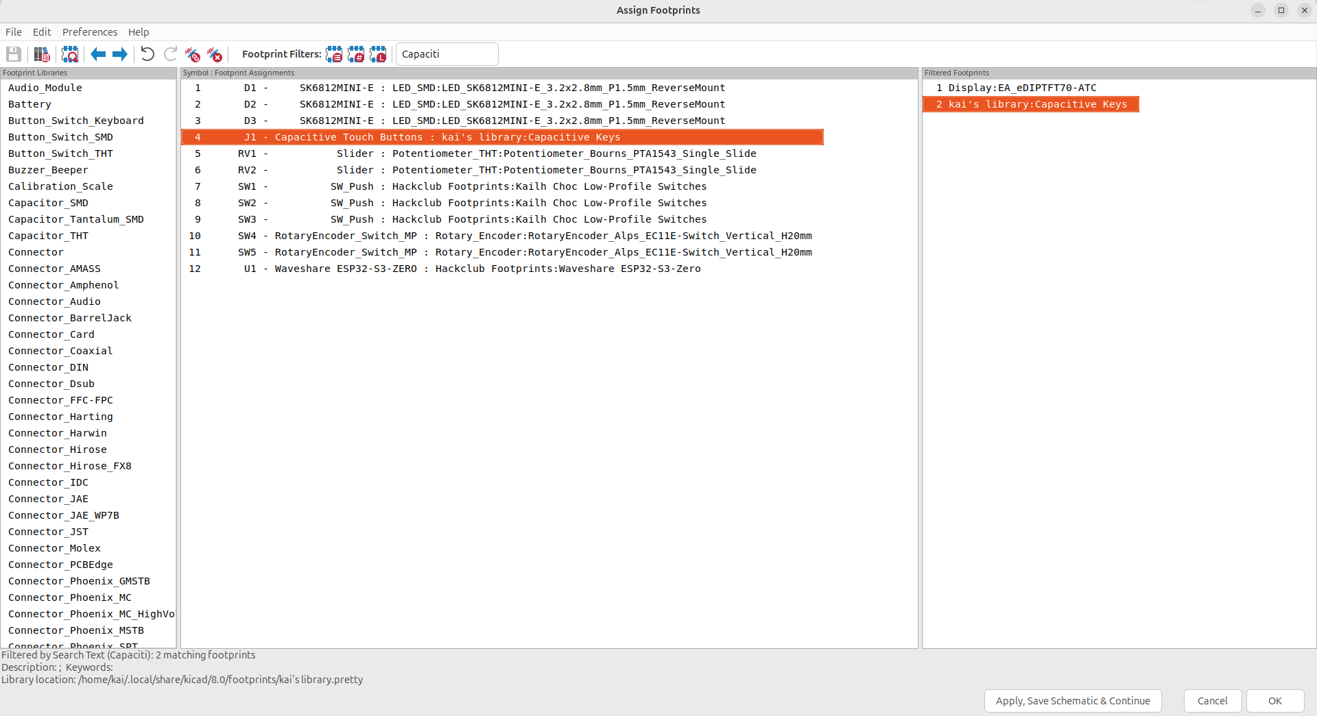
To assign the footprints, tap the "assign footprints" button in the top toolbar. Some of your symbols might already have their footprints assigned, but we still need to assign the ones we're missing:
This is what my footprints look like after:
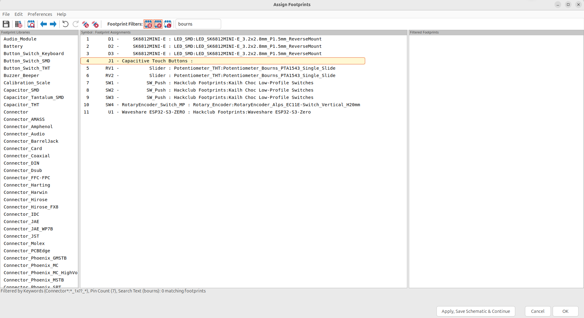
Now that you've assigned your footprints, we can start designing the actual PCB. Import all your parts by first tapping "Switch to PCB" in the top toolbar of the schematic editor, and then tap "Update PCB from Schematic" in the PCB editor and then update your PCB:
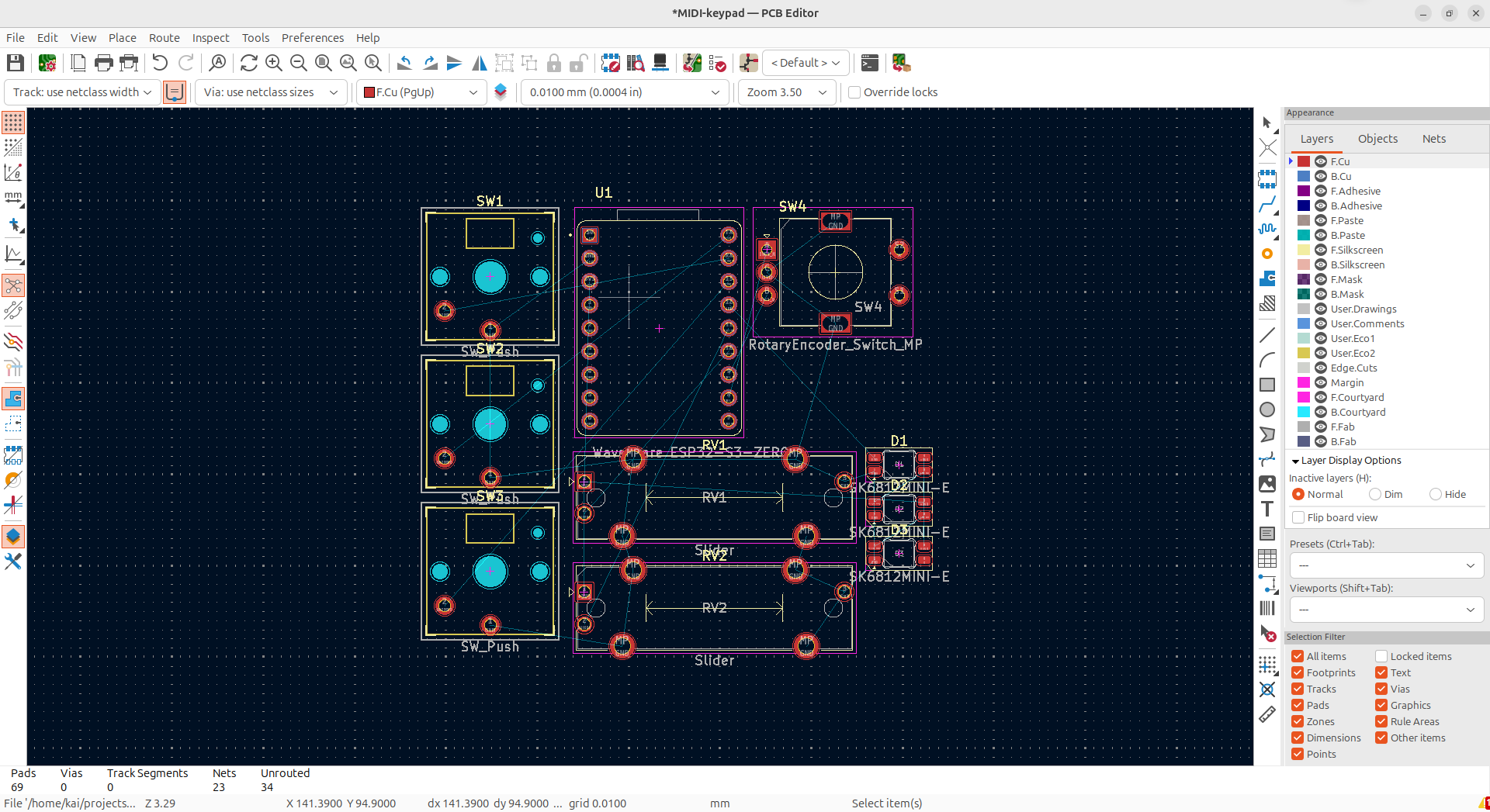
Now the only footprint we're missing is our capacitive keys! Open the KiCad footprint editor (there's a button in the top toolbar of the PCB editor for it), and then go "file -> new footprint":
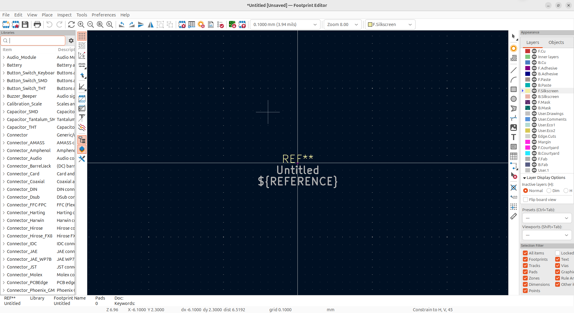
Set your grid to 1.0mm in the top toolbar, so it's easier to make precise geometry for your footprint. I would suggest changing your grid constantly to keep accurate and symmetrical geometry, don't make an ugly footprint.
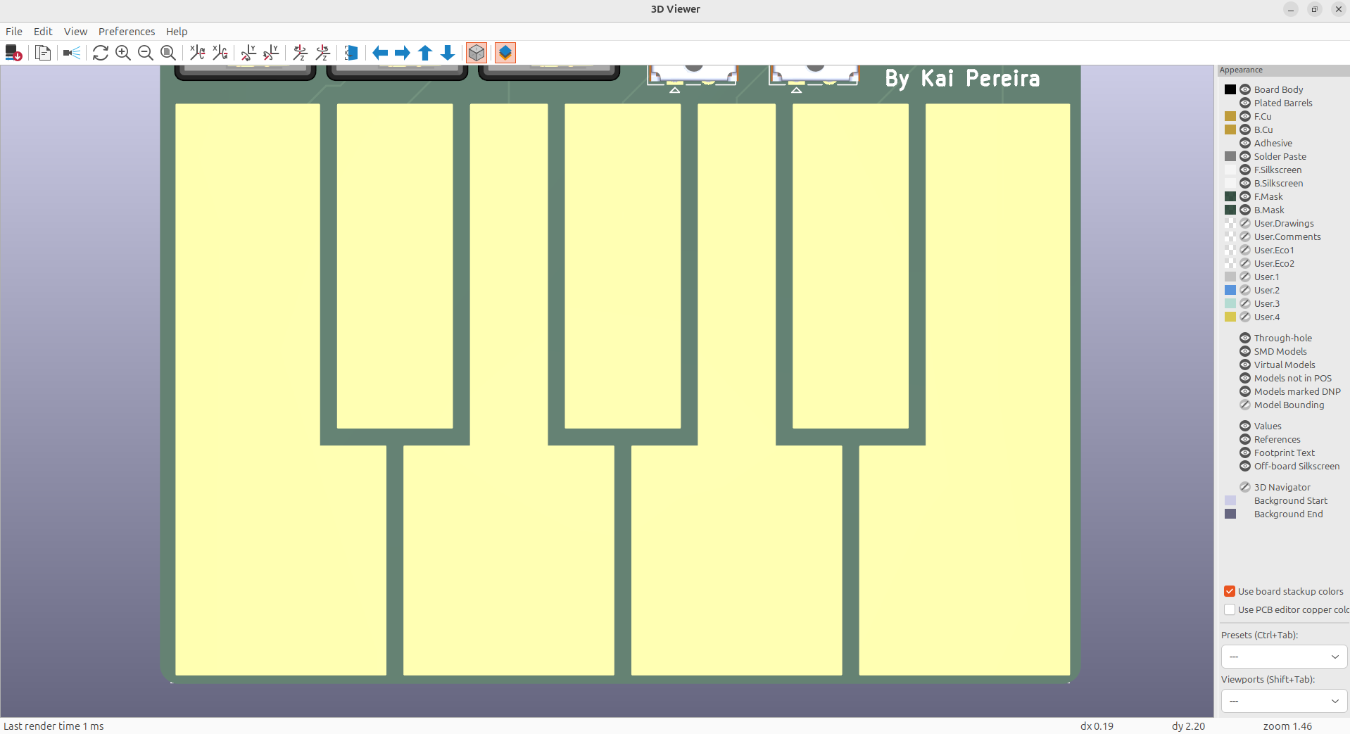
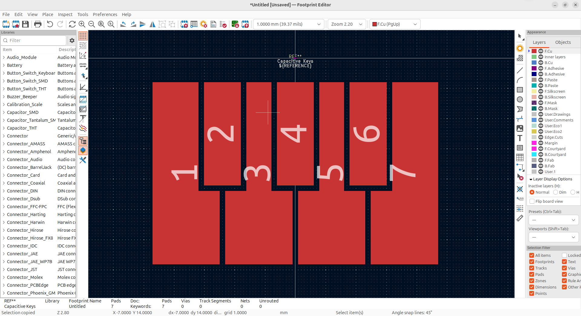
Now this is where you have a lot of freedom. You can make your capacitive keys any shape you want, squares, circles, rectangles, polygons, even drawings if you so wish (you can search up how to do so). I'm gonna make mine look like piano keys for the sake of simplicity, but go crazy.
So go to your right hand toolbar, and add a pad:
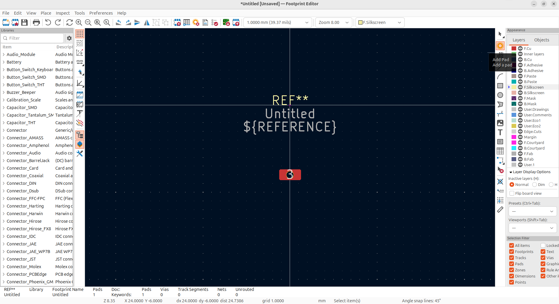
Tap your pad, and then tap "e" to bring up all of its properties. This is where you can customize your pads to look however you want but you need to do 2 things first:
Then set the pad number to 1 for the first pad, this just maps pin 1 on the symbol, to this pad of the footprint, so if you have 7 keys we'll be adding 7 pads labelled 1 through 7.
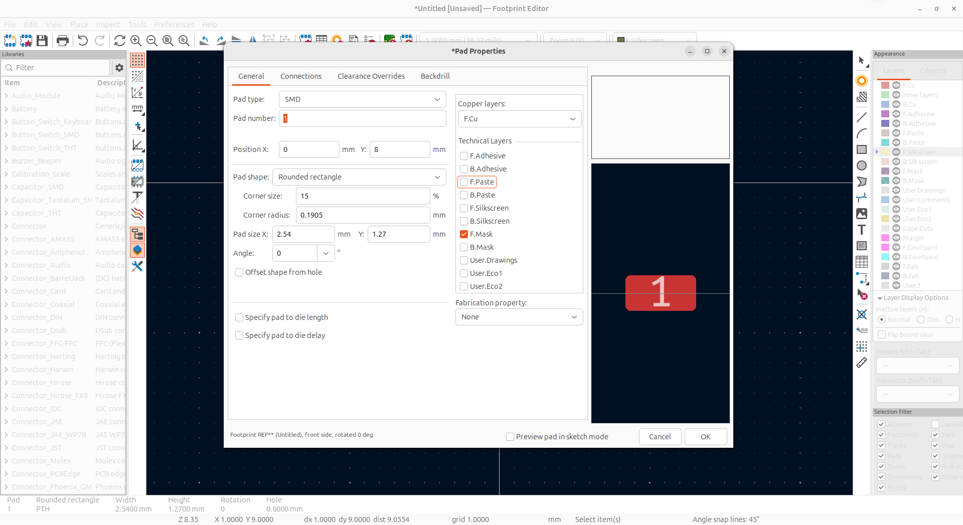
Then, you just manipulate the sizes of the pad and move them around to create your footprint. I've gone ahead and built a key footprint by using a bunch of squares and vectors, but just make your capacitive keys any shape you want, just make sure the spacing between copper is at least 0.2mm!
I'd also suggest iterating over your footprint if it doesn't fit your PCB nicely once you add it in.
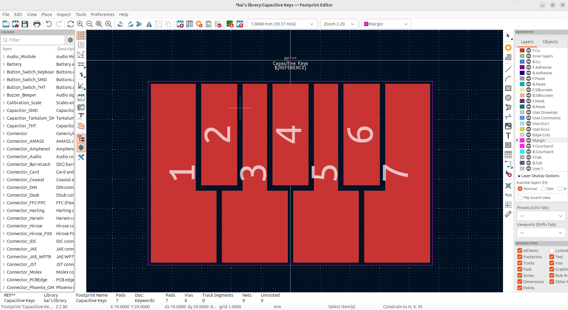
You should also add a courtyard, which just prevents you from putting components physically on-top of your footprint, but if you're careful, you don't necessarily need it, but I'd highly suggest having one: You can add one by tapping the F.Courtyard layer and then drawing something onto it.
The courtyard is the pink boundary around the footprint
Next, you'll need to create your own footprint library to save this to because the default one is read only and you don't have write permissions for it.
So go "file -> new library" and just call it whatever. I call mine "Kai's Library" and once you save it (I would also name it something like "Capacitive Keys"), you'll notice it show up in your library on the left hand side if you search for it.
Then go back to your schematic editor and assign the footprint:
Go back to the PCB editor, and then import it in using the update PCB from schematic:
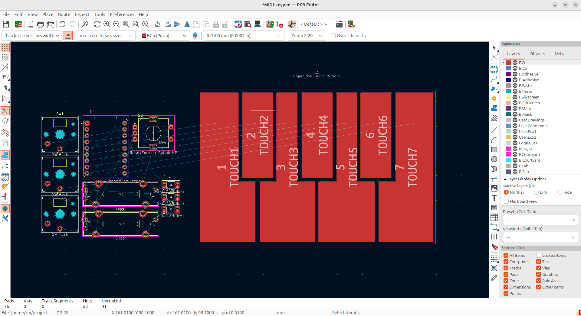
Now the first thing you want to do on your PCB is nicely lay out your components on the PCB, into the general shape you want it to look like. I'd suggest making it under 100x100mm because it makes the PCB cheaper to order, but you have complete creative freedom. Just make sure that if you have neopixels, to flip what side they are on your PCB (using "f") so that they're reverse mounted and shine through the PCB:
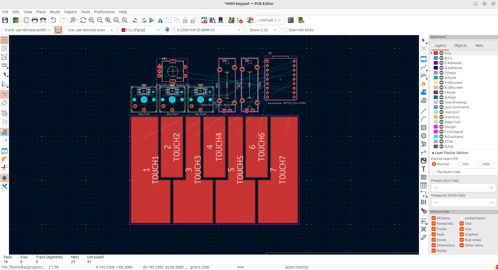
PCB design is a constantly iterative design process, so when laying out your board, routing it, etc, feel free to move stuff anytime. I would take advantage of the different grids you can use in KiCad to nicely align stuff, this board is mostly made with 1mm, 0.5mm and 0.25mm grids.
Now the first thing I'm actually going to do, is modify the net labels on my schematic so that it's easier to route the boards, and to reduce the amount of those straight blue lines/unrouted traces that we call ratsnest, intersecting:
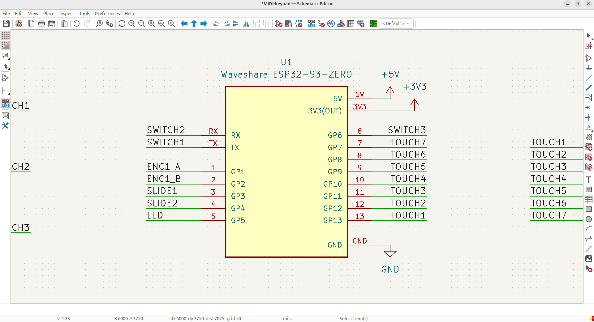
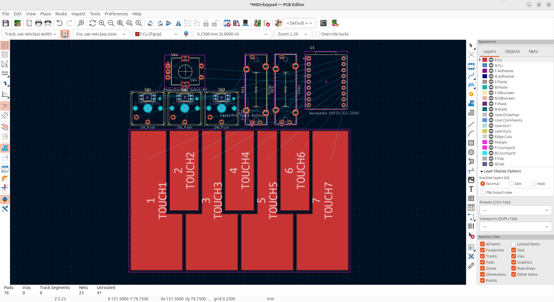
I'm quite experienced at routing PCBs so I'm pretty good at just looking at my board and doing this, but feel free to do it iteratively if you ever have weird crossing traces that aren't the prettiest.
Next, we'll add in our PCB board edge. Tap the edge.cuts layer on the right hand side, and then tap on the square or whatever shape you want your PCB. I'd suggest putting the USB-C receptacle of your MCU over the board edge so it's easy to plug in, and it'll be handy when you make the case for your keyboard. I'd also suggest rounding your edges, by tapping the outline, tapping "e" and then modifying the corner radius value so your board looks prettier:
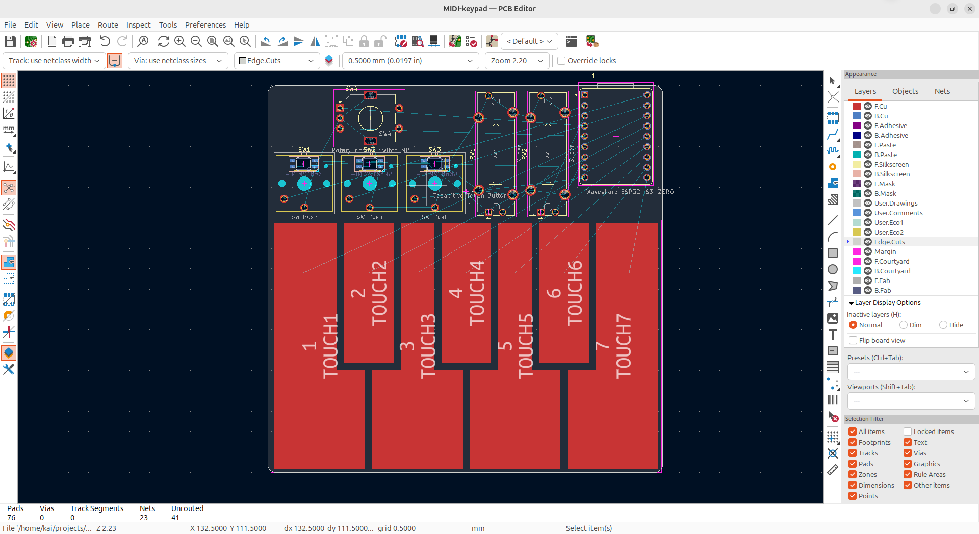
Now we get to actually route the traces for our PCB! You can tap the route button on the right hand toolbar, or you can just tap "x" to start routing. I'm not going to walk you through this, but there's a couple things you should keep in mind:
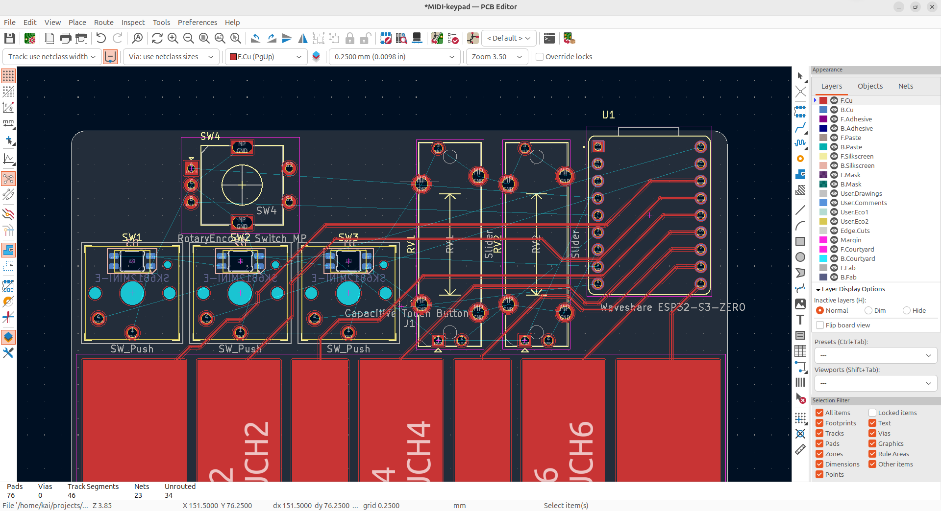
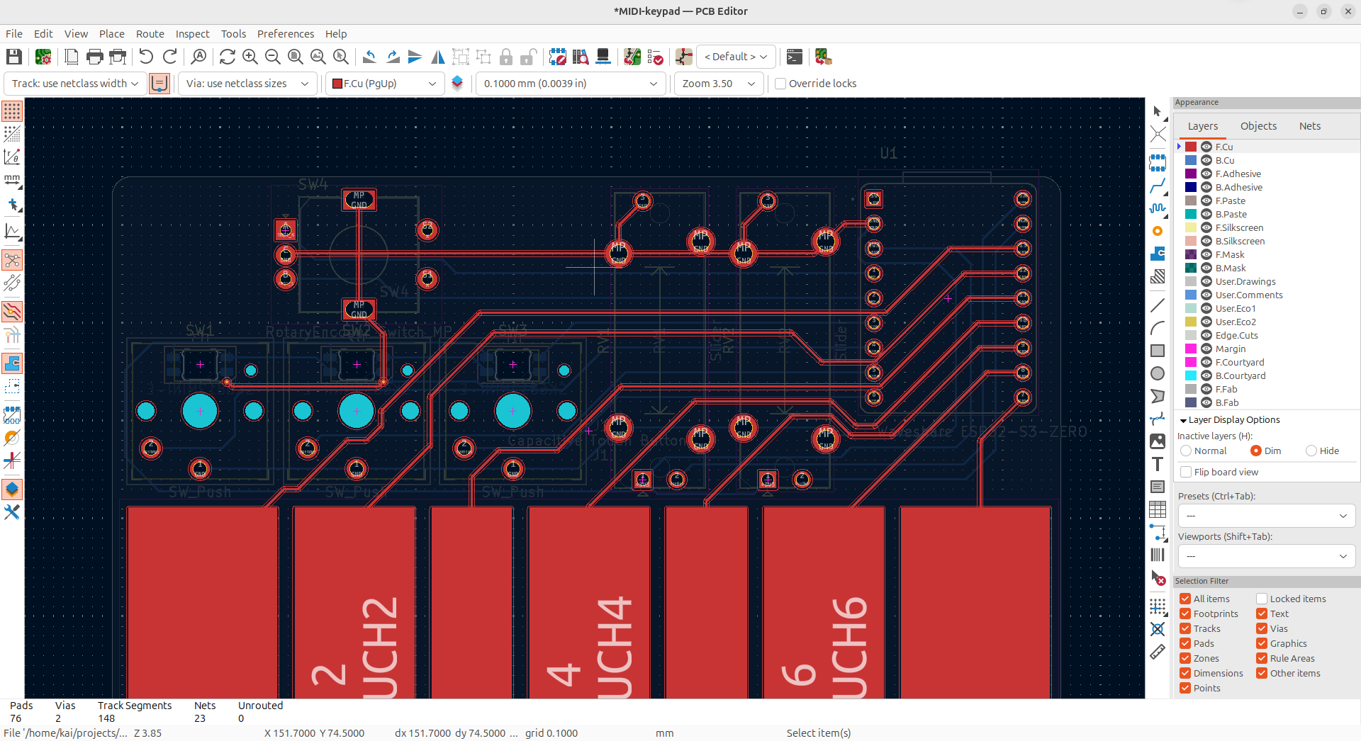
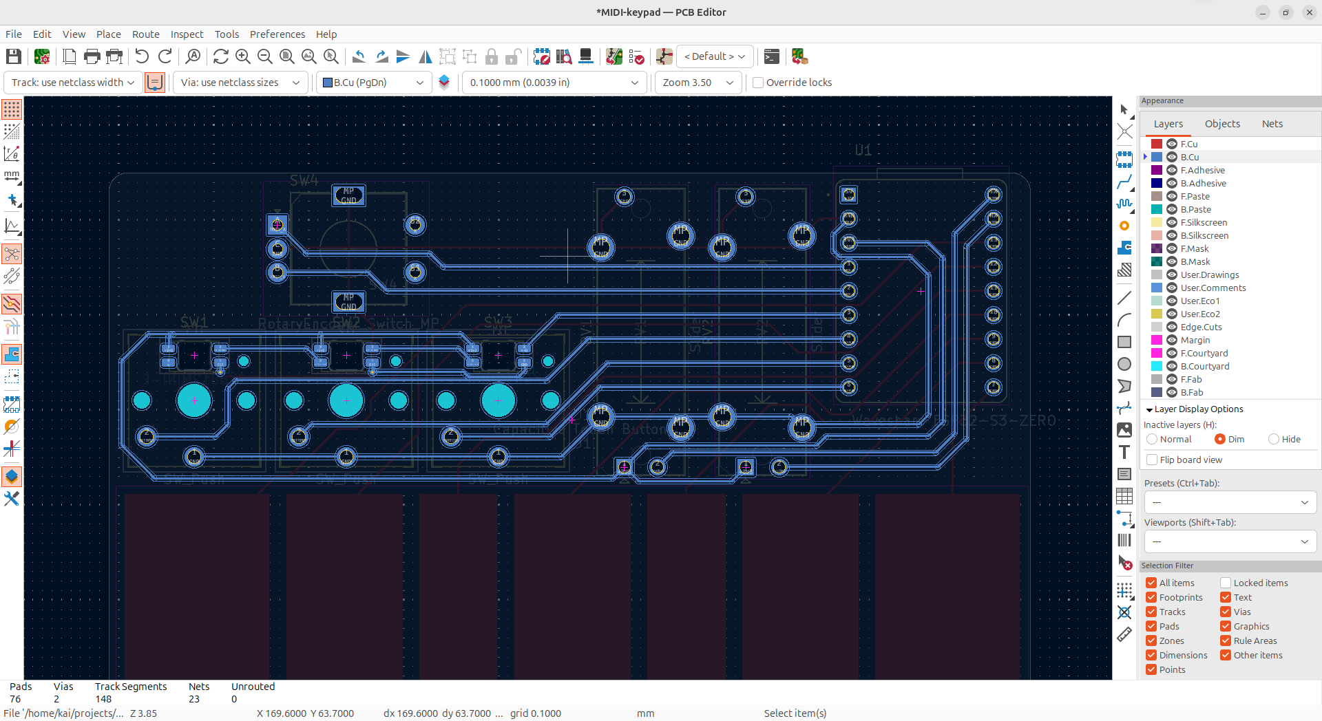
You get 2 layers to route your PCB on, the F.Cu and B.Cu layer. You can transition between these layers by placing down a via (which is essentially a tiny plated hole on your PCB) while routing on one of them, so while routing, you can just tap "v" and it'll add a via to the end of your trace, and once you place it down, you'll transition to the other layer.
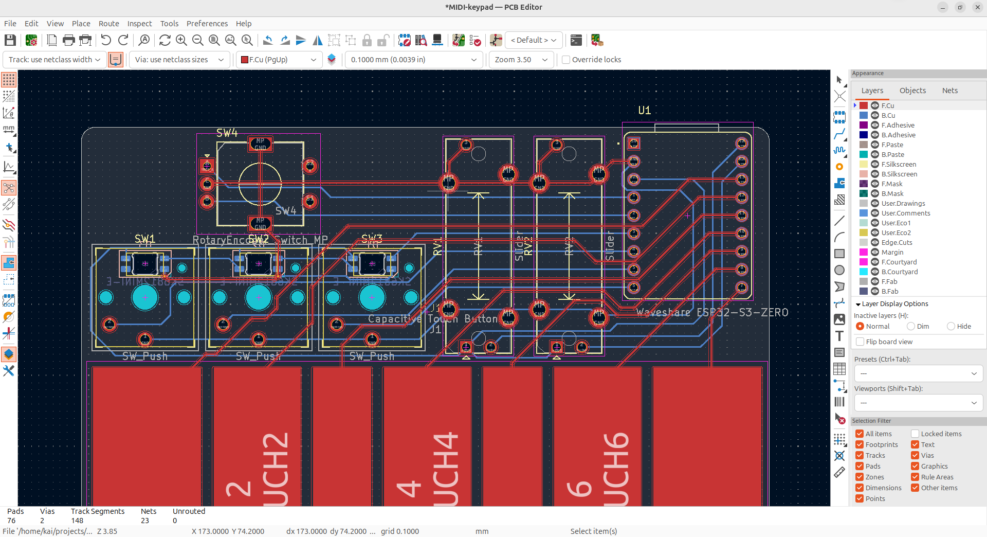
You'll want to route all of your capacitive touch keys first, and try to minimize their length, and just pay attention to them. I'd suggest routing those traces on the front layer, and then routing all the other traces on the back layer. I'm experienced at routing PCBs so don't worry if your boards are a bit uglier:
I'm a bit of a perfectionist, so this is what my final board routing looks like:
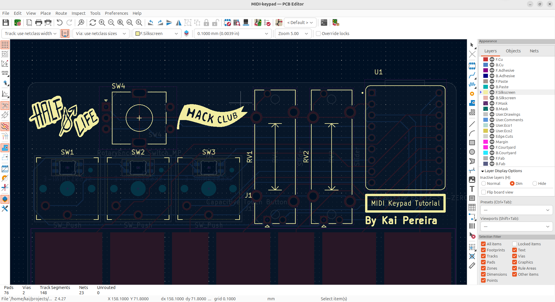
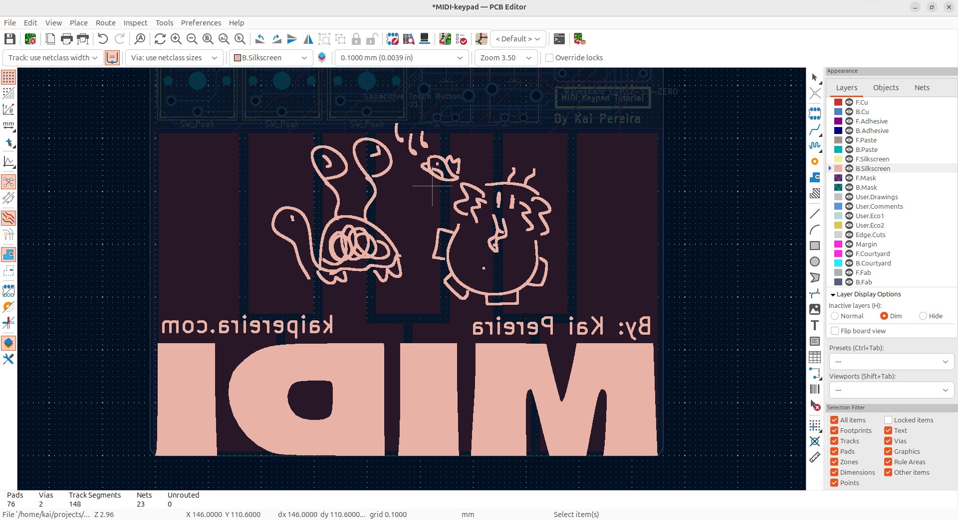
Next, it is an absolute necessity to make our PCB look beautiful by adding art. We do this by moving to the silkscreen layer! F.Silkscreen is the front art, and B.Silkscreen is the back art.
The KiCad project manager window has an image converter which is really useful for converting your images to silkscreen!
Next, we need to verify that our PCB is ready for manufacturing. We can test this by the "DRC" or design rules check in the top toolbar. So tap the button and check for errors:
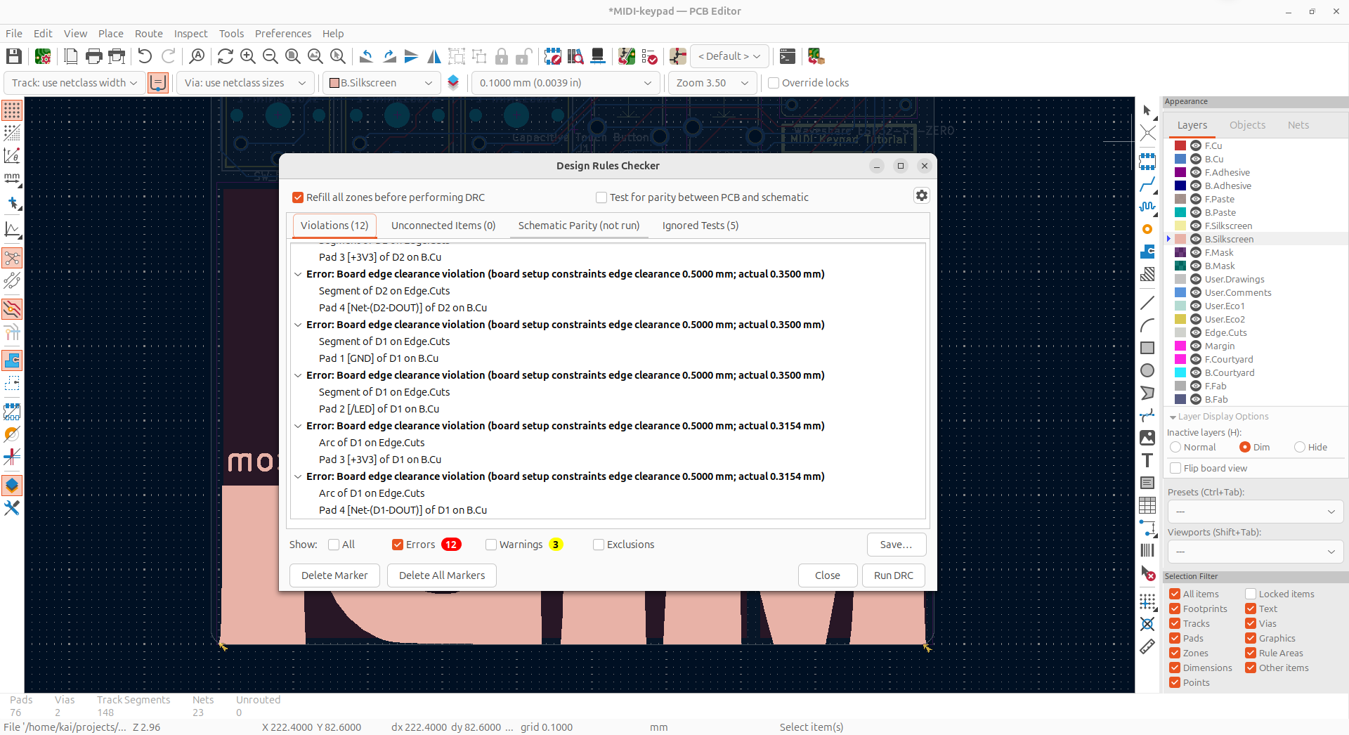
All the warnings can be ignored and same with the board edge clearance violations for the neopixels. Those are essentially just saying that our pads might be slightly cut off during manufacturing, but that's fine because they're large pads and we'll be hand-soldering them.
So if everything's good, we're onto the final steps!
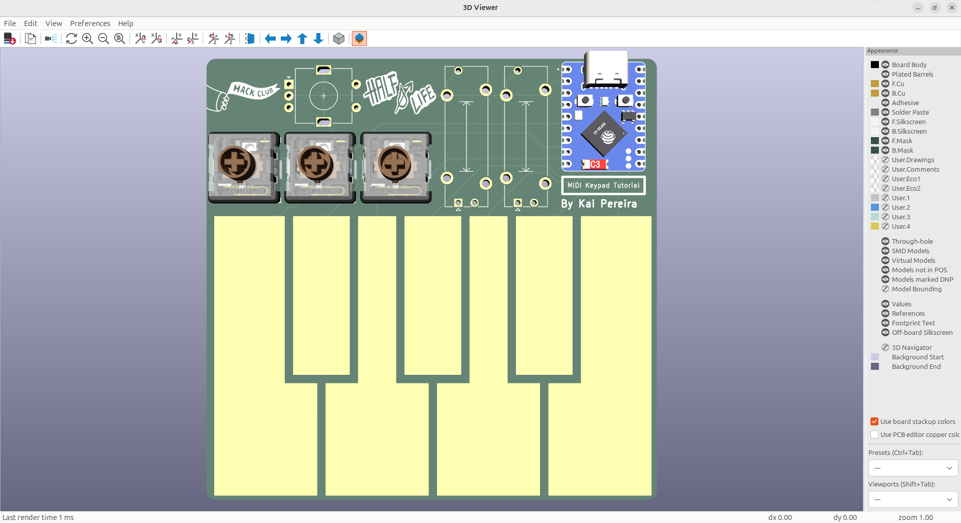
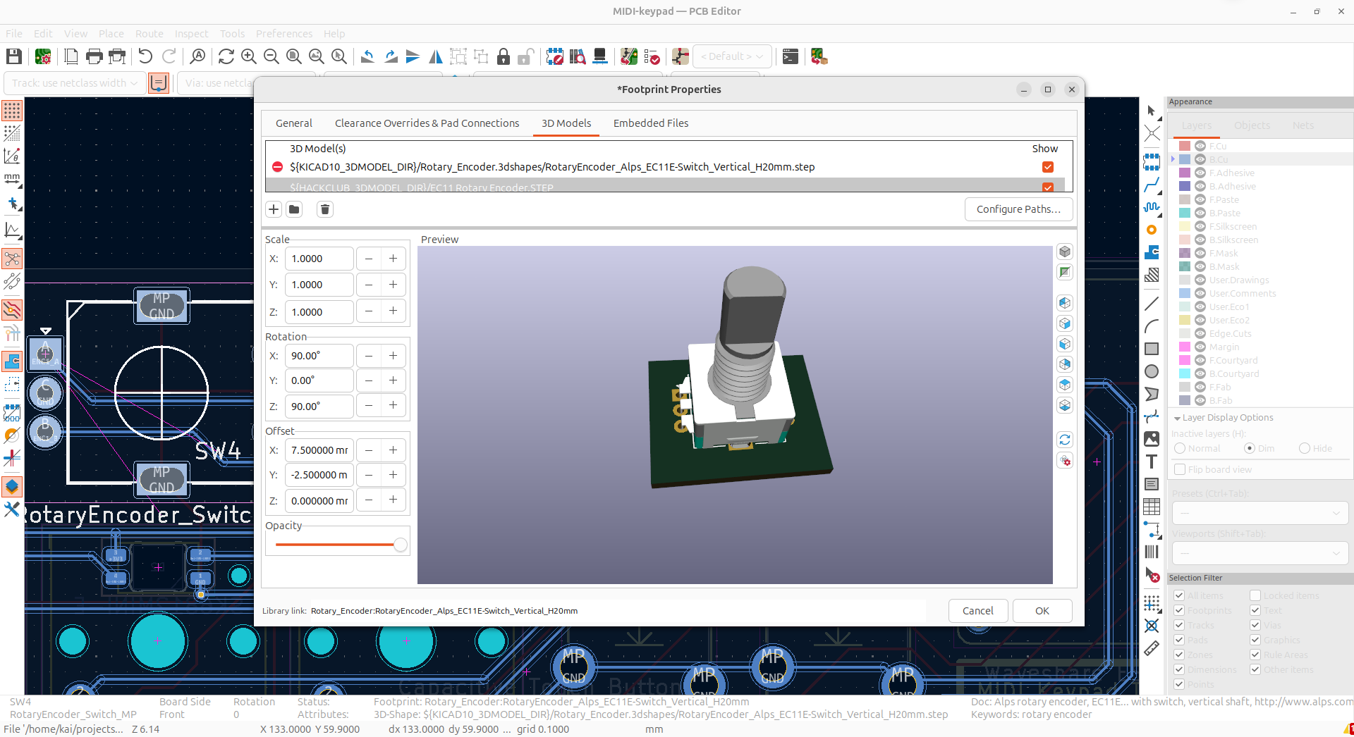
Let's add all the 3D models in for our components that don't have one yet. This will make it easier to design the case for our keypad, and will also let us take polished photos of our project. I've added all the 3D models into the GitHub repository for this tutorial, so go ahead and install the ones you need!
If you only have a couple of the component on your board, you should just tap the footprint, tap "e" and then go to the 3D model tab, and then add in the model and move it, for each footprint. But if you have quite a few of that footprint, I would suggest making a copy of the new footprint with the 3D model to your library and then just selecting it for all of that footprint on the board.
And just like that we're done our PCB!
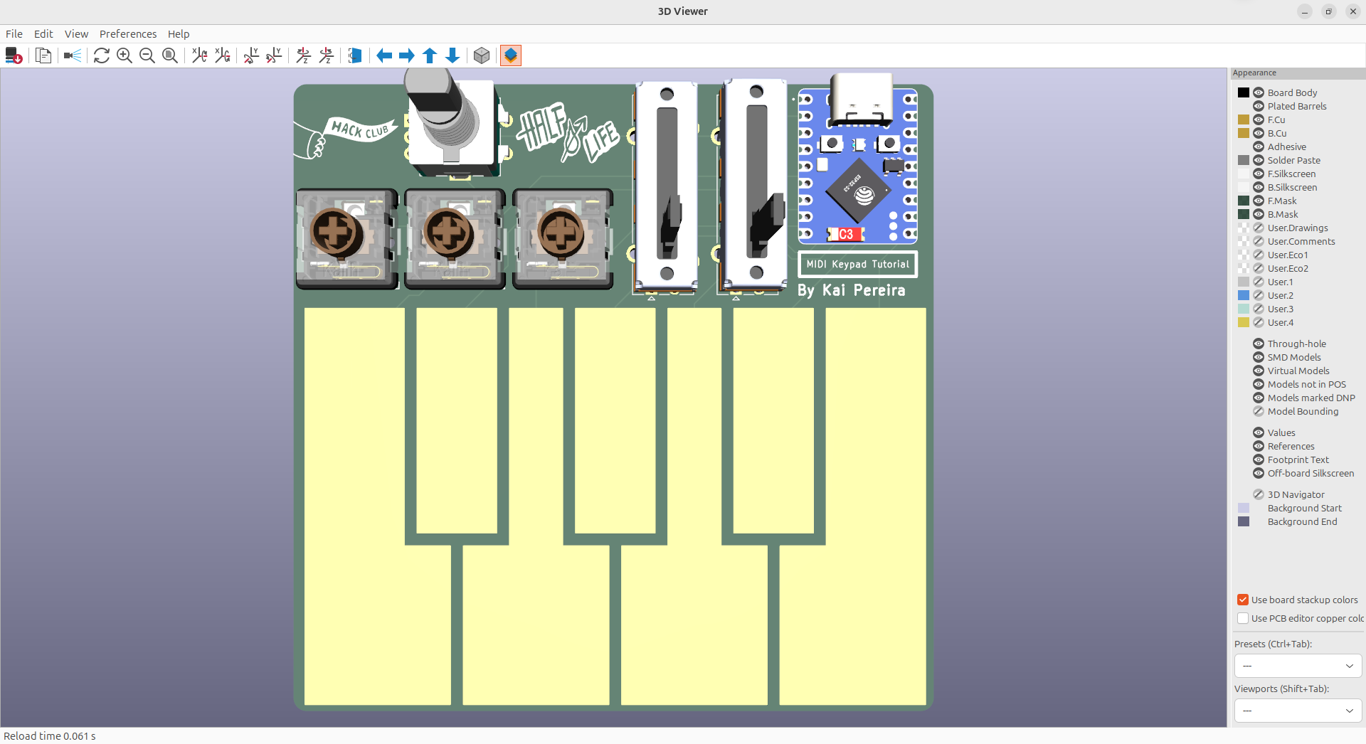
Now that we're done our PCB, we can actually prepare it for manufacturing.
Before we do anything, make sure that you've run DRC and it's clear of errors that matter, and that your PCB looks fairly polished and nice :D
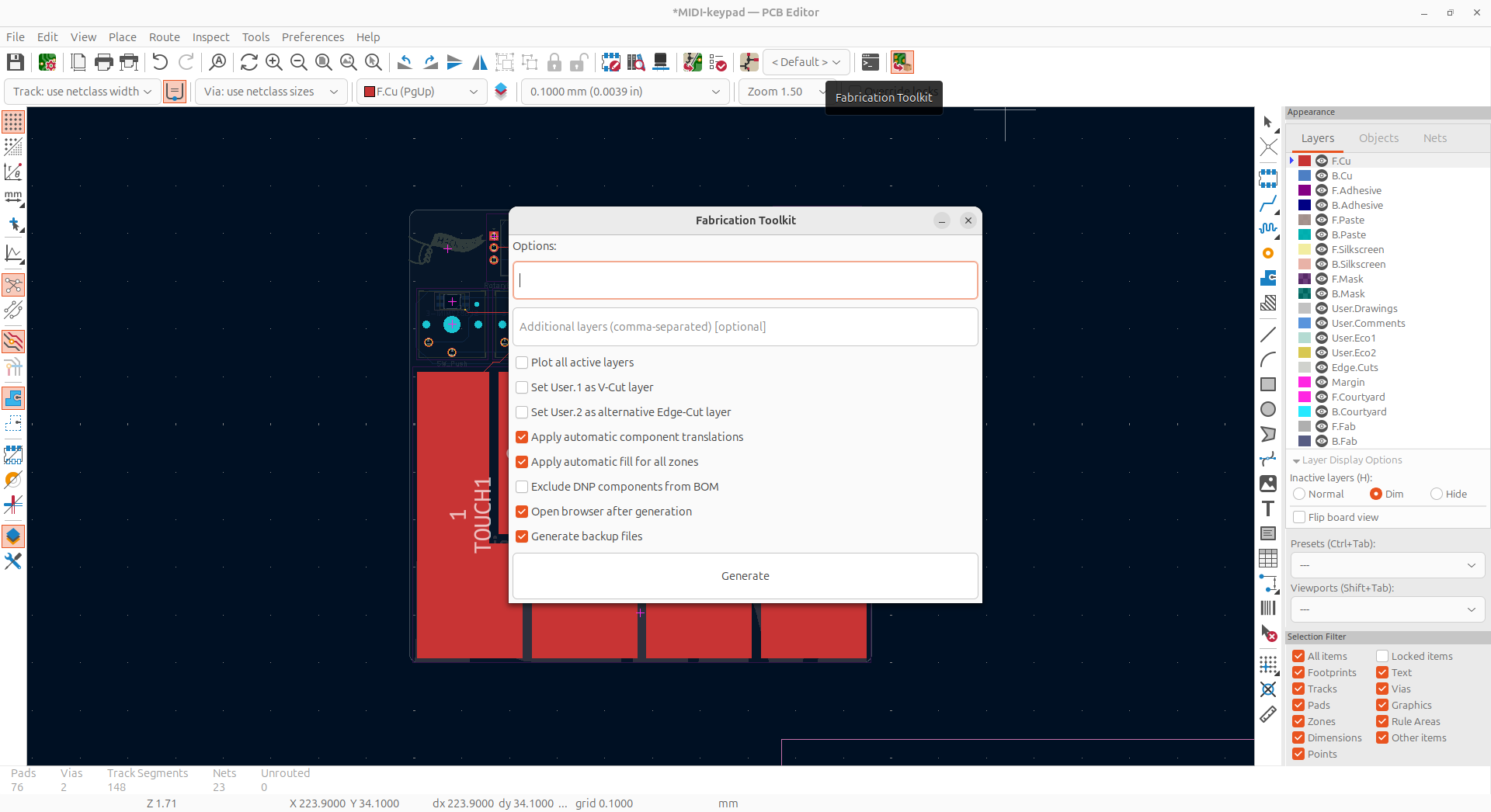
Next, we're going to install the JLCPCB fabrication toolkit, which is essentially a one-click button that exports all the files we need in order to manufacture our project. The repository nicely goes over how to install it: https://github.com/bennymeg/Fabrication-Toolkit
Once you reload KiCad, you'll see the button pop up at the end of the top toolbar, or you can go "tools -> external plugins -> Fabrication Toolkit" to open it up. And then just simply click generate and it'll make all your production files. If you ever edit your PCB again, make sure to re-generate your fabrication files:
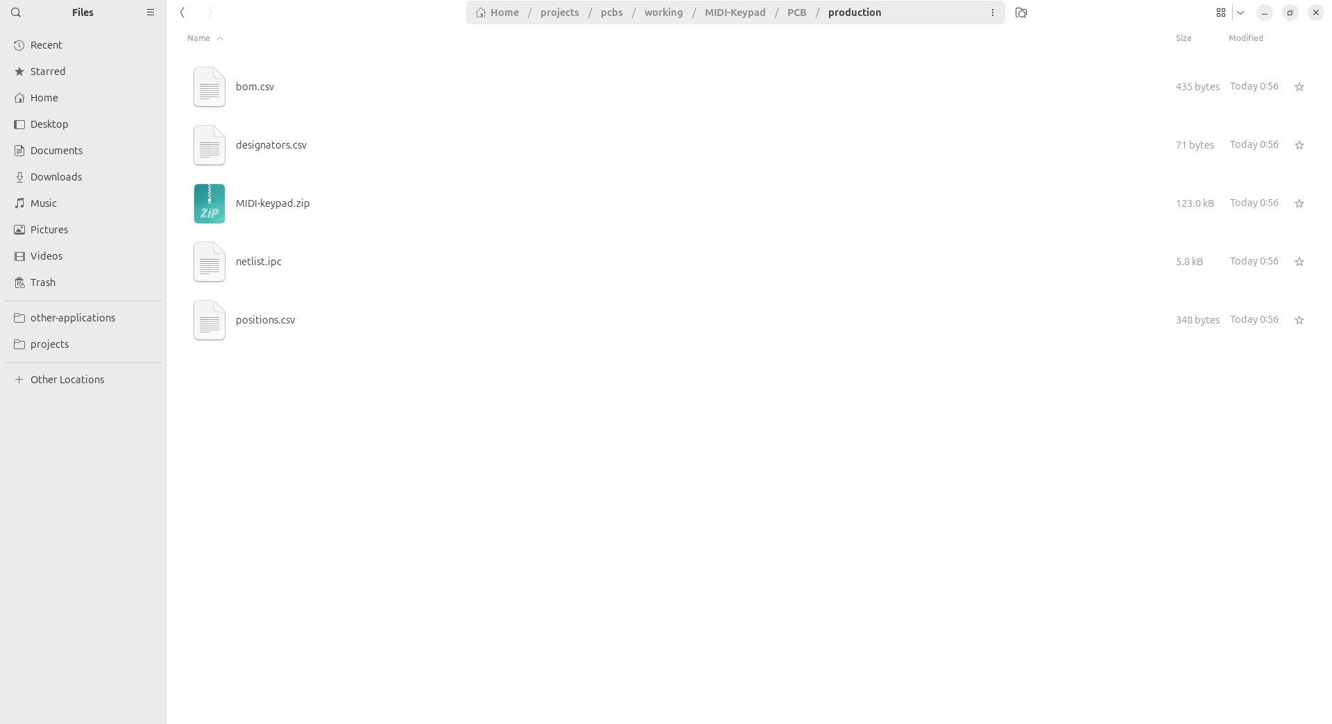
And now if you go into the /production folder it generated, you'll see the:
And there's some other files, but you don't need to worry about those.
Now we can go over to https://jlcpcb.com/ to order our PCB. Just tap order now, and then upload your gerbers zip file:
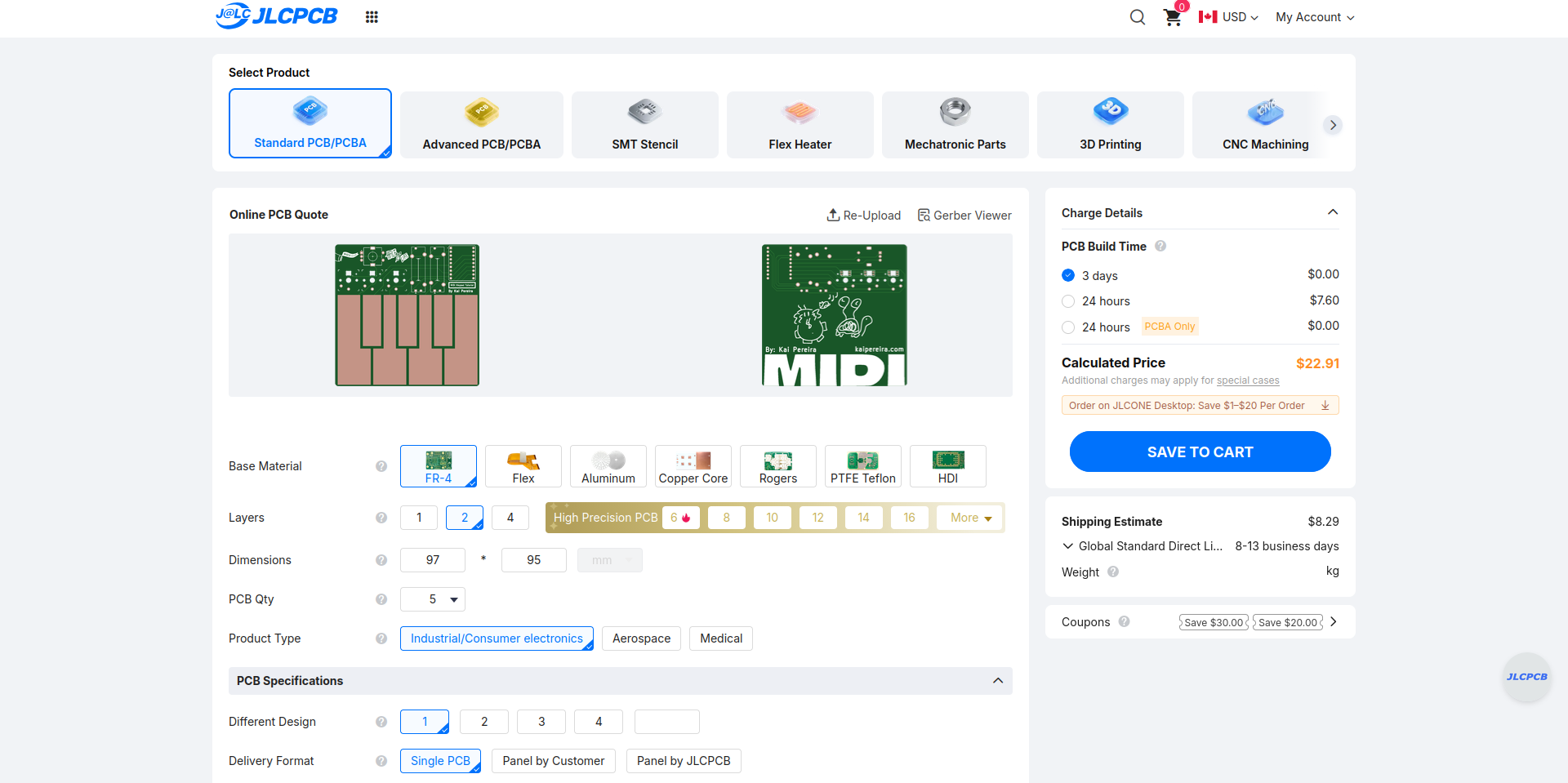
For ordering your PCB, I would suggest:
You're on the final steps, and you just have to do a couple more things to get your project ready to be shipped!
You need to make a proper BOM or Bill of Materials for your project. This is just a spreadsheet you can export as a .csv with all your parts, where you're going to buy them and their price. I would take a look at https://codex.hackclub.com/design/part-sourcing/ on how to do this!
And then you should make a basic firmware file for your project so it's easy to program once you receive your parts and have soldered your PCB. I would suggest using KMK for this but you're free to use whatever, just make sure your firmware supports the ESP32-S3.
And then finally, you need to properly ship your project. Take a look at the Codex again to see how to do this https://codex.hackclub.com/shipping/101/!
Once you receive your parts, it's relatively easy to solder them. Just watch a couple videos online on how to do so, and you'll be golden!
Congrats on making your MIDI keypad :D If you liked this tutorial, you'll probably like some of my other work too and should consider giving me a follow on GitHub and starring the repository for this tutorial.
Happy hacking, and I'd love it if you sent me your finished builds of your MIDI keypads on Slack (@Kai the Jolly Guy) or by email which you can find on my website.
| Qty | Value | Footprint | References |
|---|---|---|---|
| 4 | LOGO | LOGO | G***, G***, G***, G*** |
| 3 | SK6812MINI-E | LED_SMD:LED_SK6812MINI-E_3.2x2.8mm_P1.5mm_ReverseMount | D1, D2, D3 |
| 3 | SW_Push | Hackclub Footprints:Kailh Choc Low-Profile Switches | SW1, SW2, SW3 |
| 2 | Slider | Potentiometer_THT:Potentiometer_Bourns_PTA1543_Single_Slide | RV1, RV2 |
| 1 | Capacitive Touch Buttons | kai's library:Capacitive Keys | J1 |
| 1 | RotaryEncoder_Switch_MP | Rotary_Encoder:RotaryEncoder_Alps_EC11E-Switch_Vertical_H20mm | SW4 |
| 1 | Waveshare ESP32-S3-ZERO | Hackclub Footprints:Waveshare ESP32-S3-Zero | U1 |
google/mozc-devices
Circuit diagrams and firmware source code for Gboard DIY keyboards

Bastardkb/Dilemma
The Dilemma is a vertical stagger low-profile keyboard with mods.

Pwnsat/FlatSat
Flatsat v1.0 is a hardware based platform for aerospace cybersecurity research

adamws/kicad-kbplacer
KiCad plugin for automatic keyboard's key placement and routing

imchipwood/dumbpad
Simple 4x4 numpad with rotary encoder. Powered by QMK via ATmega32u4 Pro Micro

makerforgetech/modular-biped
An open source framework for creating a bipedal modular companion robot.


It measures 97 × 95 mm and has 2 copper layers, 1.6 mm thick.
15 parts, built around the SK6812MINI-E. The full list of its parts is on this page, with links to each part's symbol and footprint where PCBKit's library has them.
From the KaiPereira/MIDI-Keypad repository on GitHub, at the commit this page was made from: the board is PCB/MIDI-keypad.kicad_pcb and its schematic PCB/MIDI-keypad.kicad_sch. PCBKit opens the board in the browser, with nothing to install.
Its repository states no licence, so its author keeps all rights: ask KaiPereira before reusing the design.