

4 layers8.1 × 45.7 mm
Integrated PCB Design Projects
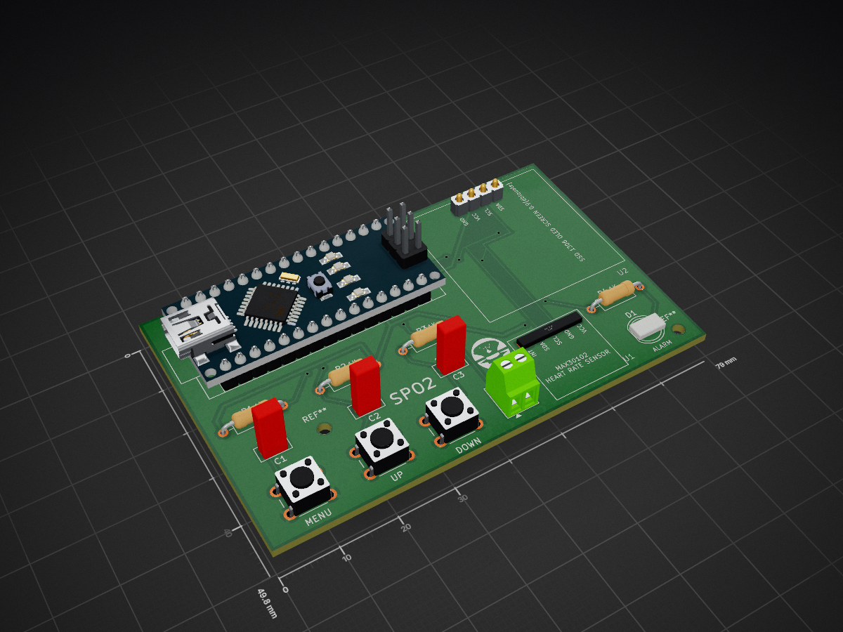
SPO2 is an open-source printed circuit board by Haylie-dt, from the Haylie-dt/PCB-Projects repository on GitHub. It is a 2-layer board of 79 × 49.8 mm with 18 parts on 32 nets, routed with 104 tracks and 13 vias.
It is built around the MAX30102. Its parts include 4 resistors, 3 capacitors, 2 ICs and 1 diode. It belongs with the AVR (ATmega, ATtiny) boards of this library.
Integrated PCB Design Projects
| Qty | Value | Footprint | References |
|---|---|---|---|
| 4 | 1k | Resistor_THT:R_Axial_DIN0207_L6.3mm_D2.5mm_P10.16mm_Horizontal | R1, R2, R3, R4 |
| 3 | 100nF_Ceramic | Capacitor_THT:C_Disc_D5.0mm_W2.5mm_P2.50mm | C1, C2, C3 |
| 3 | Push_Button | Button_Switch_THT:SW_PUSH_6mm | DOWN, MENU, UP |
| 1 | Arduino_Nano_v3.x | Module:Arduino_Nano | A1 |
| 1 | Battery | TerminalBlock:TerminalBlock_Xinya_XY308-2.54-2P_1x02_P2.54mm_Horizontal | BT1 |
| 1 | LED_5mm | LED_THT:LED_D5.0mm | D1 |
| 1 | LOGO | Images:logo3 | G*** |
| 1 | MAX30102 | Custom_spot:MAX30102_Module | U1 |
| 1 | OLED_SCREEN | Custom_spot:SSD 1306 OLED SCCREEN | U2 |
The 16 most common of 18 parts.


sandgum/Triangulate-ES_01-Watch
A 5mm thick smartwatch which uses an E-ink display and two OLEDs to display information while consuming very little power

theheraldproject/herald-hardware
Permissively licensed opensource hardware designs for Herald powered wearables and beacons. Supports digital contact tracing and other eHealth approaches.

abhinav937/RP2040_SOS_band
PCB design files for RP2040 based SmartWatch. It features an accelerometer, a GPS module and a cellular module.

Epivaral/CursoIoT
Material complementario del curso: INTRODUCCIÓN A IOT, ALMACENAMIENTO EN LA NUBE Y ANÁLISIS DE DATA

Ghost3379/NX-ISD
A more sophisticated version of the Artemis Watch by Circuitmess.


Soham3126/DIY-SPO2-KiCAD-Project
A low-cost, non-invasive Pulse Oximeter (SpO2) and Heart Rate monitor based on the MAX30102 sensor and Arduino. This project features real-time PPG signal processing, I2C communication, and a custom PCB design for…

Taller-de-sistemas-embebidos-tps/tdse-tf_2-01
Trabajo Final - Taller de Sistemas Embebidos - FIUBA
It measures 79 × 49.8 mm and has 2 copper layers, 1.6 mm thick.
18 parts, built around the MAX30102. The full list of its parts is on this page, with links to each part's symbol and footprint where PCBKit's library has them.
From the Haylie-dt/PCB-Projects repository on GitHub, at the commit this page was made from: the board is SPO2/SPO2.kicad_pcb and its schematic BMS SMD/1S BMS SMD Mode.kicad_sch. PCBKit opens the board in the browser, with nothing to install.
Its repository states no licence, so its author keeps all rights: ask Haylie-dt before reusing the design.