Skip to the content
2 layers29.5 × 53.6 mmESP32 S2 Breakout, the printed circuit board in 3D

Breakout Board for ESP32 S2 Solo

Size
29.5 × 53.6 mm
Copper layers
2
Thickness
1.6 mm
Parts
41
Nets
73
Pads
242
Tracks, vias
791, 69
Pours
2
Routed
Yes
KiCad
KiCad 7 (file 20221018)
Created
13 Apr 2024
Updated
13 Apr 2024

Overview

ESP32 S2 Breakout is an open-source printed circuit board by EzerLonginus, from the EzerLonginus/ESP32_S2_SOLO_Breakout repository on GitHub, published under the GPL-3.0 licence. It is a 2-layer board of 29.5 × 53.6 mm with 41 parts on 73 nets, routed with 791 tracks and 69 vias.

It is built around the AMS1117-3.3 and TPD1E05U06QDPYRQ1. Its parts include 12 capacitors, 12 resistors, 5 diodes, 3 ICs and 3 connectors. It belongs with the interfaces and adapters boards and the ESP32 boards of this library.

Main components

2

README

README.md

ESP32_S2_SOLO_Breakout

Breakout Board for ESP32 S2 Solo

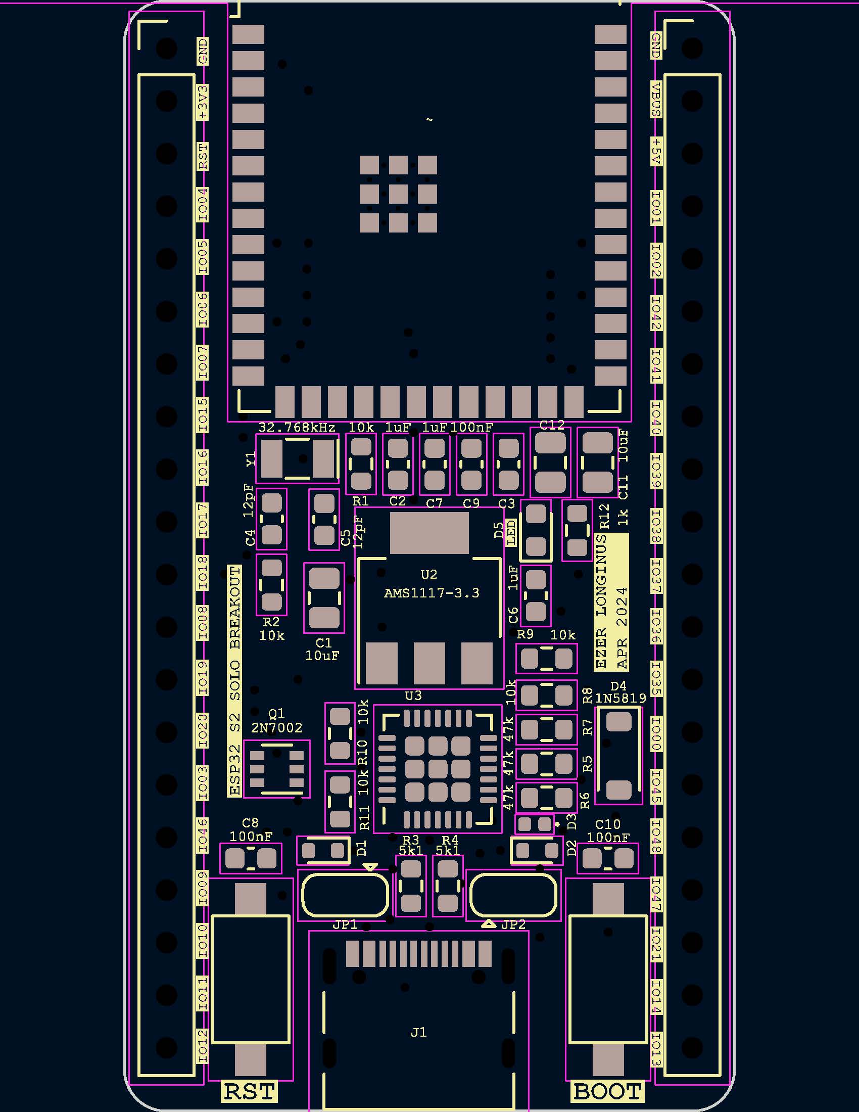
This board is a simple breakout for the ESP32 S2 Solo. The interface includes the standard reset and boot button, with a USB to UART CP2012 converter, and a 3V3 regulator. Also included is an LED on the GPIO 0 pin. All GPIO pins are broken out to standard 2.54mm headers. USB-C reseptacle connector is used, but at the USB 2.0 standard.

Purpose

This is mostly an excersize in designing an ESP32 module for inclusion in other projects. Once this design is functional, I'll start using it as a template for more custom oriented projects involving the chip (or some variant). I decided on the ESP S2 Solo, mostly because it was fairly inexpensive and I didn't see too many other breakouts utilizing it. Depending on how this excersize goes, I may start designing boards with just the bare chip (no built in WiFi antenna, SPI Flash, etc).

Scematic
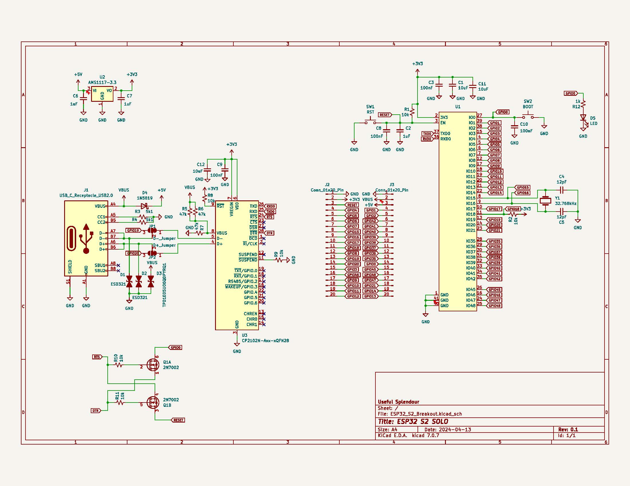
ESP32 S2 Solo Schematic

Layout

ESP32 S2 Solo Layout

Current State of Affairs

Version 1

  • Populate and test board
  • Upload some blink/hello world sketch
  • Fix the inevitable issue that I missed during production

Static Badge

Parts

41
QtyValueFootprintReferences
610kResistor_SMD:R_0603_1608MetricR1, R2, R8, R9, R10, R11
4100nFCapacitor_SMD:C_0603_1608MetricC3, C8, C9, C10
310uFCapacitor_SMD:C_0805_2012MetricC1, C11, C12
31uFCapacitor_SMD:C_0603_1608MetricC2, C6, C7
347kResistor_SMD:R_0603_1608MetricR5, R6, R7
212pFCapacitor_SMD:C_0603_1608MetricC4, C5
25k1Resistor_SMD:R_0603_1608MetricR3, R4
2Conn_01x20_PinConnector_PinHeader_2.54mm:PinHeader_1x20_P2.54mm_VerticalJ2, J3
2ESD321Diode_SMD:D_SOD-523D1, D2
11N5819Diode_SMD:D_SOD-123D4
11kResistor_SMD:R_0603_1608MetricR12
12N7002Package_TO_SOT_SMD:SOT-363_SC-70-6Q1
132.768kHzCrystal:Crystal_SMD_MicroCrystal_CC7V-T1A-2Pin_3.2x1.5mmY1
1AMS1117-3.3Package_TO_SOT_SMD:SOT-223-3_TabPin2U2
1BOOTButton_Switch_SMD:SW_SPST_CK_RS282G05A3SW2
1CP2102N-Axx-xQFN28Package_DFN_QFN:QFN-28-1EP_5x5mm_P0.5mm_EP3.35x3.35mmU3
1D+_JumperJumper:SolderJumper-3_P1.3mm_Bridged2Bar12_RoundedPad1.0x1.5mmJP2
1D-_JumperJumper:SolderJumper-3_P1.3mm_Bridged2Bar12_RoundedPad1.0x1.5mmJP1
1LEDLED_SMD:LED_0603_1608MetricD5
1RSTButton_Switch_SMD:SW_SPST_CK_RS282G05A3SW1
1TPD1E05U06QDPYRQ1Diode_SMD:D_0402_1005MetricD3
1USB_C_Receptacle_USB2.0Connector_USB:USB_C_Receptacle_G-Switch_GT-USB-7010ASVJ1
1~RF_Module:ESP32-S3-WROOM-1U1

Similar boards

  • 4 layers53.5 × 65.5 mmChipigniteExplain, the printed circuit board in 3D

    ChipigniteExplain

    efabless/chipignite_discover

    This FPGA experimentation and development board was developped for efabless chipignite workshops and labs to serve as an easy to use experimentation board and stepping stone towards ASIC digital design, allowing for…

    251 parts2Apache-2.0
  • 2 layers290.1 × 130 mmPro V2, the printed circuit board in 3D

    Pro V2

    kata0510/Lily58

    6×4+4keys column-staggered split keyboard.

    312 parts2.3k
  • 2 layers26.2 × 45.5 mmPL18 multiprotocol, the printed circuit board in 3D

    PL18 multiprotocol

    pascallanger/DIY-Multiprotocol-TX-Module

    Multiprotocol TX Module (or MULTI-Module) is a 2.4GHz transmitter module which controls many different receivers and models.

    24 parts1.9kGPL-3.0
  • 4 layers99 × 53.3 mmPSLab, the printed circuit board in 3D

    PSLab

    fossasia/pslab-hardware

    PSLab Hardware Design and Schematics https://pslab.io

    199 parts1.7kApache-2.0
  • 4 layers85 × 56 mmPslab mini, the printed circuit board in 3D

    Pslab mini

    fossasia/pslab-mini-hardware

    PSLab Mini Hardware https://pslab.io

    182 parts1.2kApache-2.0
  • 4 layers100 × 54 mm32Bit shift register, the printed circuit board in 3D

    32Bit shift register

    MaltWhiskey/Mega-Cube

    16x16x16 PL9823 Cube with Teensy 4.0 and FlexIO driver

    64 parts766
  • 2 layers44.2 × 29.3 mmI2c tiny usb, the printed circuit board in 3D

    I2c tiny usb

    harbaum/I2C-Tiny-USB

    Cheap and simple I²C to USB interface

    27 parts454
  • 2 layers78 × 60 mmIce viz, the printed circuit board in 3D

    Ice viz

    muni-works/vcad

    BRep CAD kernel in Rust/WASM

    44 parts442Apache-2.0

Questions

How big is the ESP32 S2 Breakout PCB?

It measures 29.5 × 53.6 mm and has 2 copper layers, 1.6 mm thick.

What parts does the ESP32 S2 Breakout use?

41 parts, built around the AMS1117-3.3 and TPD1E05U06QDPYRQ1. The full list of its parts is on this page, with links to each part's symbol and footprint where PCBKit's library has them.

Where can I download the ESP32 S2 Breakout KiCad files?

From the EzerLonginus/ESP32_S2_SOLO_Breakout repository on GitHub, at the commit this page was made from: the board is hardware/ESP32_S2_Breakout/ESP32_S2_Breakout.kicad_pcb and its schematic hardware/ESP32_S2_Breakout/ESP32_S2_Breakout.kicad_sch. PCBKit opens the board in the browser, with nothing to install.

Can I use the ESP32 S2 Breakout design in my own project?

Its repository publishes it under the GPL-3.0 licence: you may reuse it on that licence's terms (keep the author's notice, and for a copyleft licence share your changes alike).