4 layers98 × 101.6 mm
Impedance Analyzer V2
EliMattingly22/Simple_Impedance_Analyzer
A PCB impedance analyzer to measure loads to 100kHz and beyond
90 parts12MIT

 EliMattingly22/Simple_Impedance_Analyzer12
A PCB impedance analyzer to measure loads to 100kHz and beyond
Impedance Analyzer V3 is an open-source printed circuit board by EliMattingly22, from the EliMattingly22/Simple_Impedance_Analyzer repository on GitHub, published under the MIT licence. It is a 2-layer board of 94.4 × 90 mm with 92 parts on 61 nets, routed with 457 tracks and 263 vias.
It is built around the INA129P, LM358 and BUF634T, with the L7805 and MUX509ID among its other parts. Its parts include 27 capacitors, 26 resistors, 17 connectors, 6 ICs and 6 diodes. It belongs with the sensors and measurement boards of this library.


The impedance analyzer was designed as a low-cost, flexible, and accurate platform to perform impedance measurement at arbitrary frequencies up to ~250kHz. The current infrastructure assumes the user has access to a National Instruments DAQ (e.g. NI-USB-6363), though similar digitizers would be similarly effective.
In this current configuration:
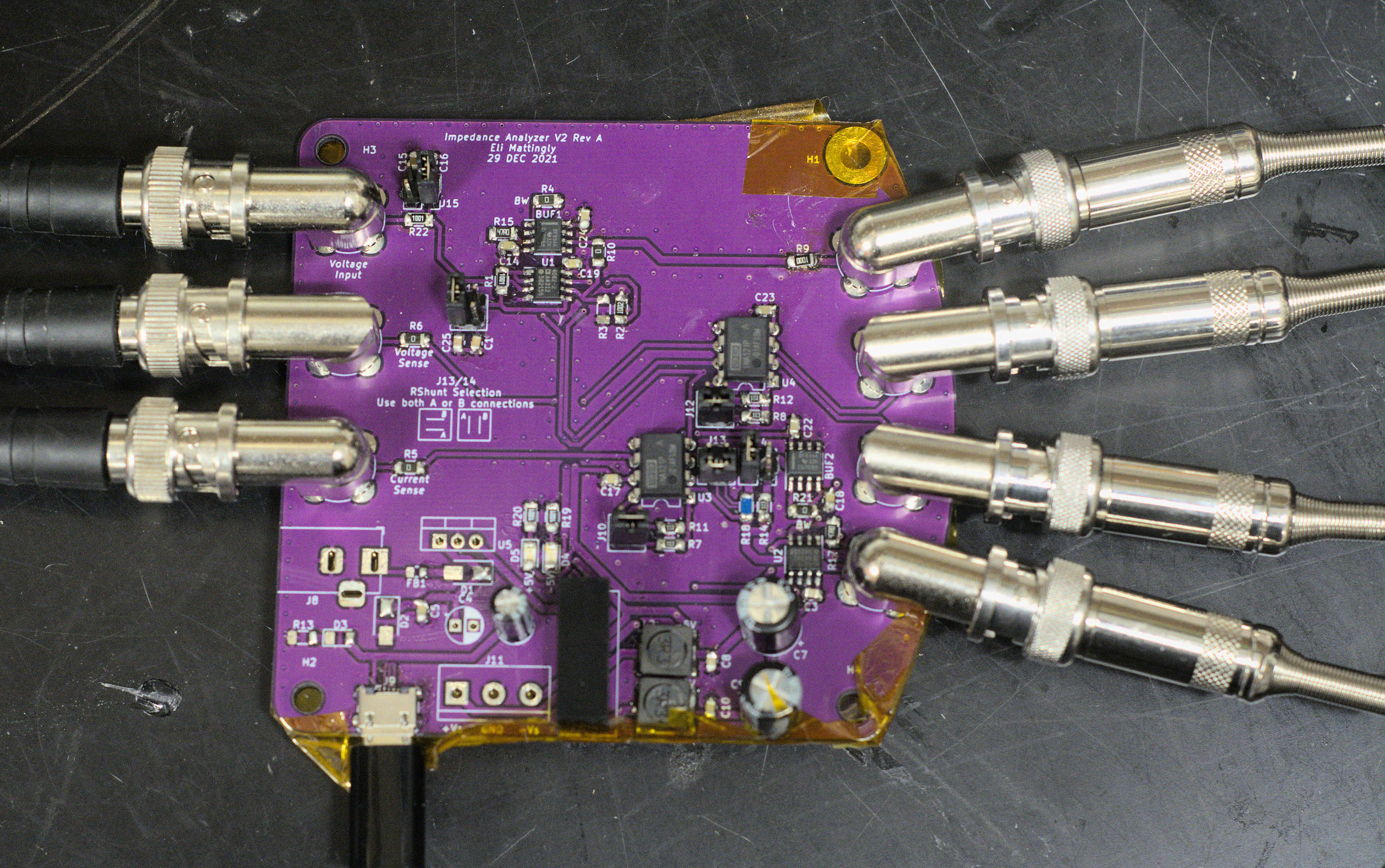
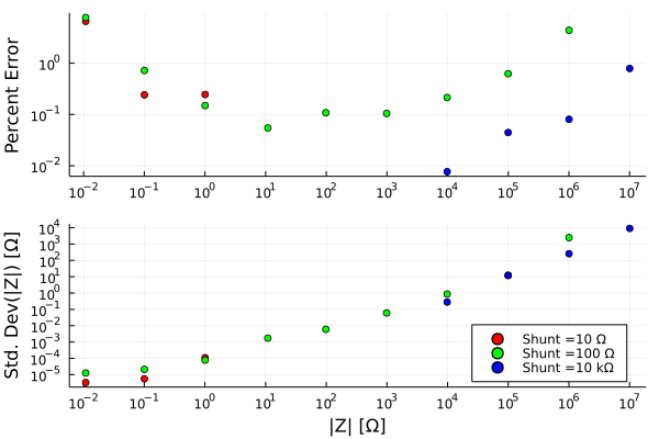
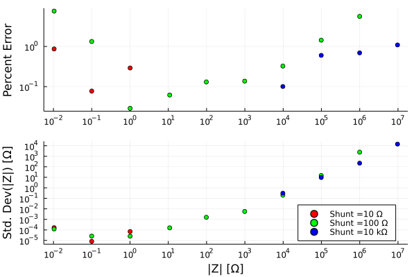
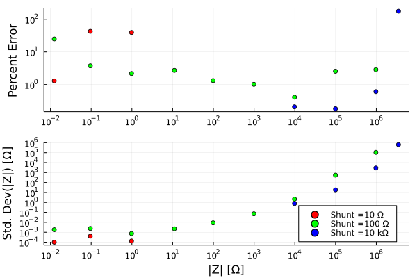
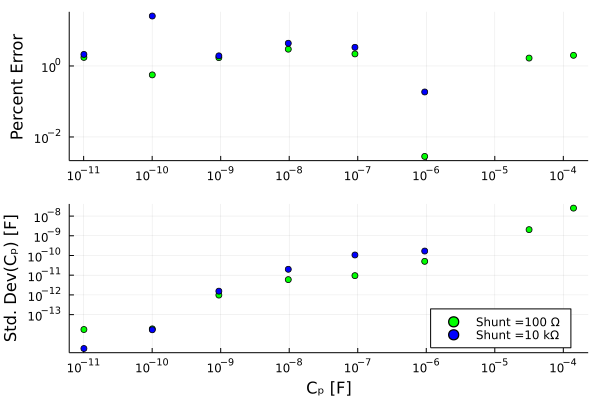
Use V2 rev B. V3 has not been tested/built. it is still in design phase. Perhaps it should just be in a separate brach of Github. Designed in KiCAD v6.
This circuit uses the "auto-balancing bridge" technique. If you are curious/want to play around with the circuit you can see the LTSPICE schematic.
It is worth reading the Keysight impedance measurement handbook or TI's reference design for an LCR meter front-end for an overview of measurement techniques.
The current through the DUT is (ideally) the same as the current in the shunt resistor, so the impedance is V(DUT) / (V(Shunt)/R(Shunt)).
The precision of the circuit is dominated by the shunt resistors and gain accuracy of the INAs. Error in any of these will linearly cause an error in the calculated impedance. If they are stable over time, they can conceivably be calibrated with a high tolerance (e.g. 0.01%) reference resistor.
If the shunt resistor is off by some value, X (where 1.01 would be 1% higher than nominal), the current would be reported as I0*X where I0 is the actual current.
The noise performance of the INAs isn't great, but the FET inputs have extremely low bias currents, and low current noise, which are necessary if high impedance loads are attached. The noise should add an incoherent error, so by averaging for longer, this can be mitigated.
The parasitic elements can be accounted for by taking an open/short/load measurement. See sect. 4.3.2 in the impedance measurement handbook
The device should be plugged in with a four-wire (Kelvin) probe attached. On the probe there will be two pairs of leads, each connected to a clamp (typically one pair is red, one is black). The two BNC connections on the red lead should be plugged into the "HPot" and "HCur" connectors, and the BNCs on the black probe should be connected to "LPot" and "HPot" connectors.
Plug in the power and make sure the LEDs next to the "+5V" and "-5V" are illuminated.
The DAQ should be plugged in via the BNC connectors and however they are connected, those outputs/inputs are selected on the front page of the Labview GUI.
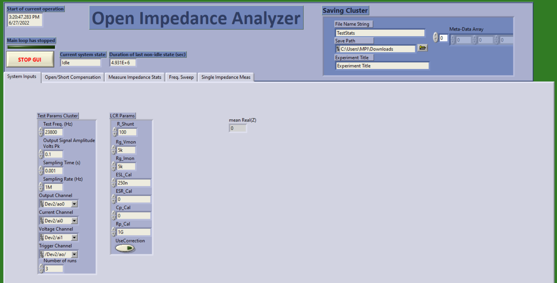
Also on the front page, set the sampling rate to the maximum allowable (see documentation for your DAQ). Set the sampling time to be >10 periods of whatever frequency you are testing at. Longer gives better noise performance.
For the shunt resistor, use the value most similar to the load you are measuring. Use J13/14 to select the shunt resistor.
Set the series resistor before the load (R9/24) to the same value as the shunt resistor using J17.
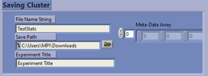
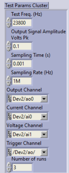
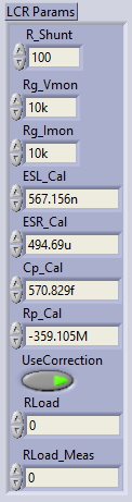
R_Shunt: The shunt resistor value (R14/18)
Rg_Vmon: The gain-setting resistor for the voltage monitor (R12 or R8)
Rg_Imon: The gain-setting resistor for the current monitor (R11 or R7)
ESL_Cal: This value is set by the short circuit compensation and is enabled by the UseCorrection boolean
ESR_Cal: This value is set by the short circuit compensation and is enabled by the UseCorrection boolean
Cp_Cal: This value is set by the open circuit compensation and is enabled by the UseCorrection boolean
Rp_Cal: This value is set by the open circuit compensation and is enabled by the UseCorrection boolean
UseCorrection: enables the short/open compensation values. Typically set to TRUE (green illuminated)
RLoad: This is the actual value of the load compensation resistor that one may use to calibrate gain errors of the system.
RLoad_Meas: This is the measured value of that load. To acquire this value, set RLoad and RLoad_Meas to 0 and then measure the known load and set this and the RLoad by typing in the appropriate values.
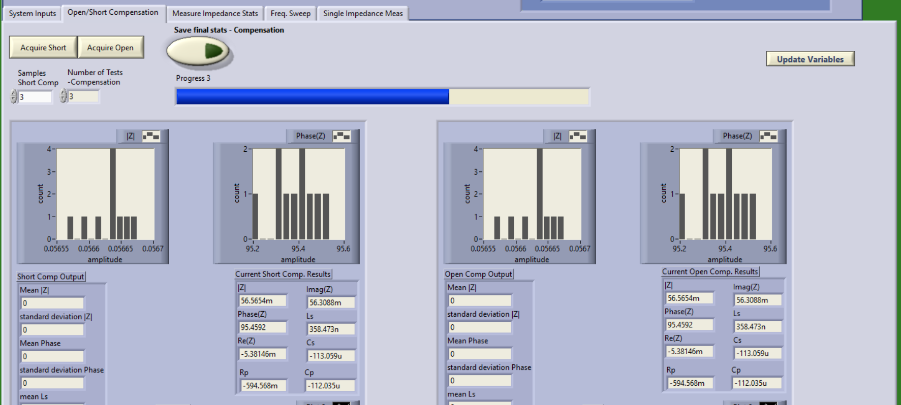
Set the equipment up to measure your load, and short the clips together. Next, go to the Short/Open compensation tab and press the "Acquire short" button. Open the clips and then do the open compensation.
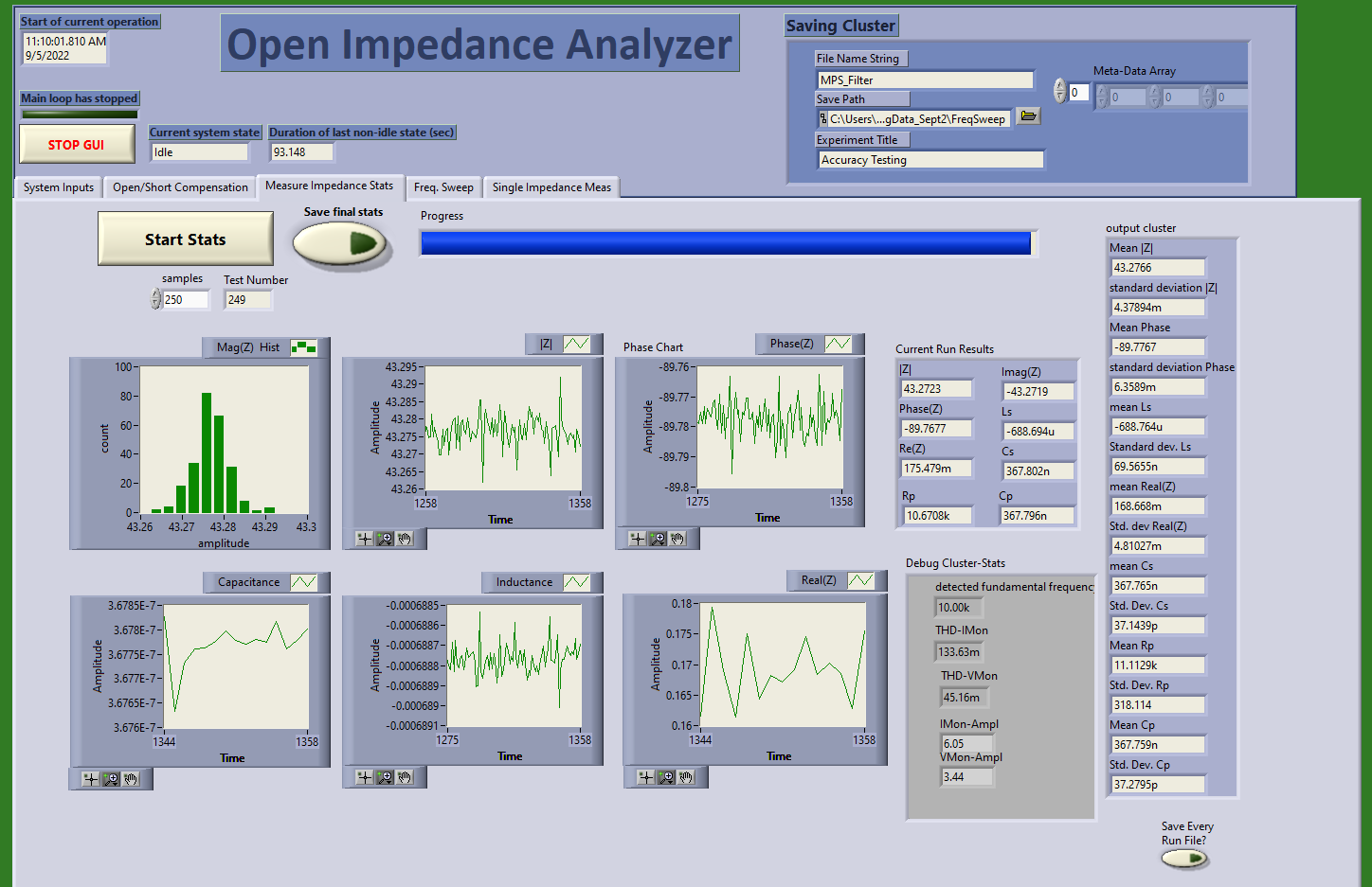
Use the last page to do a single impedance measurement and ensure the load is similar to expected. Then use the stats page or freq sweep depending on what you want.
J15/16 low-pass filters for the input. These clean the analog signal from the DAQ. They can generally be set to the highest frequency that the user plans to measure. Removing the jumper disconnects the filtering entirely.
J10: The current monitor gain selection
J12: Voltage monitor gain selection
J13/14: Shunt resistor selection
J17: Series resistor selection. This resistor in series with the load helps stability and makes the system more balanced. The resistor value should match the shunt resistor value.
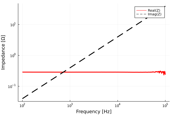
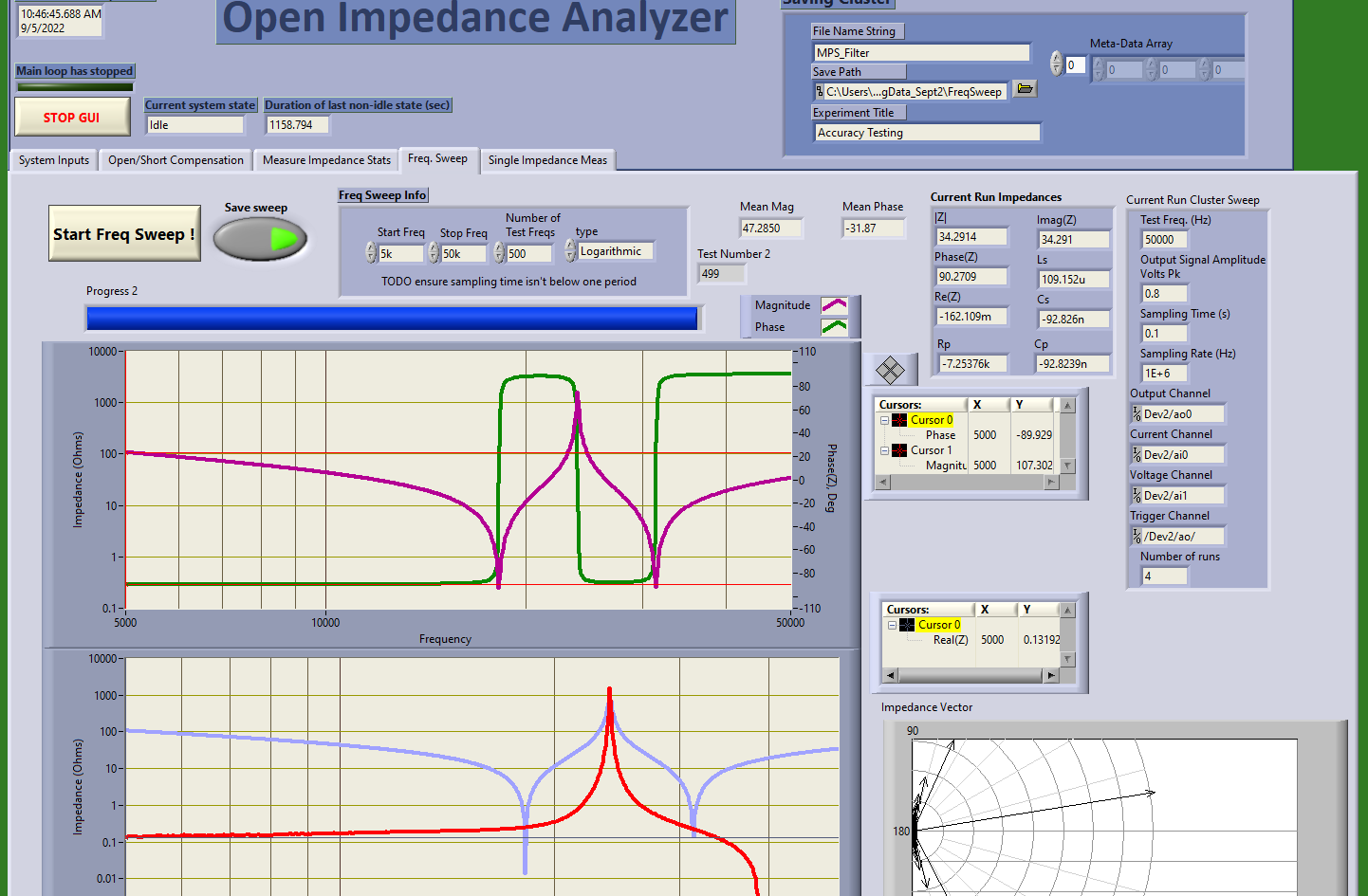
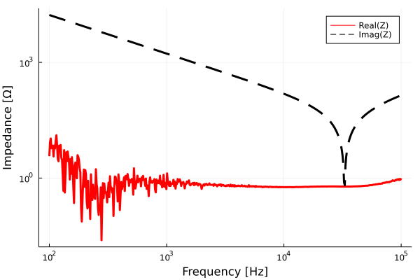
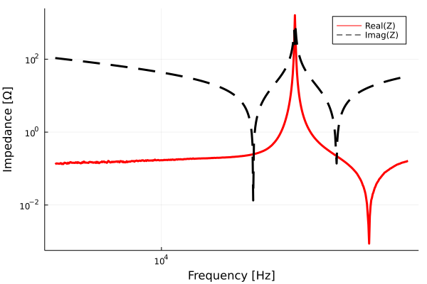
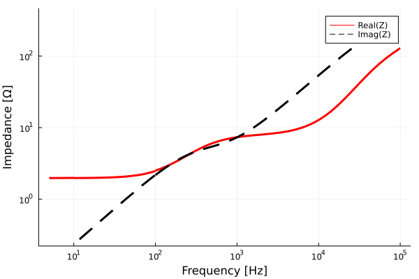 This is a frequency sweep of a solenoid (~1 mm diameter) wound on a copper tube with a wall-thickness of ~1 mm. Quite a lot is happening with this load:
| Qty | Value | Footprint | References |
|---|---|---|---|
| 15 | 100n | Capacitor_SMD:C_0805_2012Metric | C3, C5, C8, C10, C14, C17, C18, C19, C20, C21, C22, C23, C24, C26, C27 |
| 8 | 1k | Resistor_SMD:R_1206_3216Metric | R1, R11, R12, R13, R19, R20, R22, R25 |
| 7 | Conn_Coaxial | Connector_Coaxial:BNC_TEConnectivity_1478204_Vertical | J1, J2, J3, J4, J5, J6, J7 |
| 6 | 10k | Resistor_SMD:R_1206_3216Metric | R2, R7, R8, R14, R16, R24 |
| 6 | Conn_02x02_Counter_Clockwise | Connector_PinHeader_2.54mm:PinHeader_2x02_P2.54mm_Vertical | J10, J12, J13, J14, J15, J16 |
| 4 | C_Polarized | Capacitor_Tantalum_SMD:CP_EIA-6032-20_AVX-F_Pad2.25x2.35mm_HandSolder | C2, C11, C12, C13 |
| 3 | 100 | Resistor_SMD:R_1206_3216Metric | R9, R18, R26 |
| 3 | DNP | Resistor_SMD:R_1206_3216Metric | R3, R4, R21 |
| 3 | LED | LED_SMD:LED_1206_3216Metric | D3, D4, D5 |
| 3 | MountingHole | MountingHole:MountingHole_4mm | H2, H3, H4 |
| 2 | 10n | Capacitor_SMD:C_0805_2012Metric | C16, C25 |
| 2 | 10u | Inductor_SMD:L_Taiyo-Yuden_NR-60xx_HandSoldering | L1, L2 |
| 2 | 1n | Capacitor_SMD:C_0805_2012Metric | C1, C15 |
| 2 | 22u | Capacitor_THT:CP_Radial_D5.0mm_P2.50mm | C4, C6 |
| 2 | 47 | Resistor_SMD:R_1206_3216Metric | R5, R6 |
| 2 | 50 | Resistor_SMD:R_1206_3216Metric | R15, R17 |
| 2 | BUF634 | Package_SO:SO-8_3.9x4.9mm_P1.27mm | BUF1, BUF2 |
| 2 | CP | Capacitor_THT:CP_Radial_D8.0mm_P5.00mm | C7, C9 |
| 2 | D_TVS | Diode_SMD:D_SMA | D2, D6 |
| 2 | INA129 | Package_DIP:DIP-8_W7.62mm | U3, U4 |
| 2 | LM358 | Package_SO:SO-8_3.9x4.9mm_P1.27mm | U1, U2 |
| 2 | Screw_Terminal_01x03 | TerminalBlock:TerminalBlock_bornier-3_P5.08mm | J11, J17 |
| 1 | 0 | Resistor_SMD:R_1206_3216Metric | R10 |
| 1 | 100k | Resistor_SMD:R_1206_3216Metric | R23 |
| 1 | Barrel_Jack_Switch | Connector_BarrelJack:BarrelJack_Horizontal | J8 |
| 1 | D | Diode_SMD:D_SMA | D1 |
| 1 | DPUN02L-XX | Martinos:SIP-2W-7 | Reg1 |
| 1 | Ferrite_Bead | Resistor_SMD:R_0805_2012Metric | FB1 |
| 1 | L7805 | Package_TO_SOT_THT:TO-220-3_Vertical | U5 |
| 1 | MUX509ID | Package_SO:SOIC-16_3.9x9.9mm_P1.27mm | U6 |
| 1 | MountingHole_Pad | MountingHole:MountingHole_4.3mm_M4_Pad | H1 |
| 1 | USB_B_Micro | Connector_USB:USB_Micro-B_Wuerth_629105150521 | J9 |
EliMattingly22/Simple_Impedance_Analyzer
A PCB impedance analyzer to measure loads to 100kHz and beyond

EliMattingly22/Simple_Impedance_Analyzer
A PCB impedance analyzer to measure loads to 100kHz and beyond

EliMattingly22/Simple_Impedance_Analyzer
A PCB impedance analyzer to measure loads to 100kHz and beyond


JayBernstein/EMG-Controlled-Prosthetic
Senior Project for Dr. Pernalete at Cal Poly Pomona, Fall 2023 - Spring 2024


TU-Darmstadt-APQ/RedPitaya-Lockbox
Digital controller for laser frequency stabilization based on the RedPitaya STEMlab 125-14 board

JQIamo/20A-bipolar-current-source
20A bipolar current source with water cooled sensing resistor

Konat23/RTD_Thermometer
A system that allows to measure and visualize the temperature using a thermal resistance sensor (RTD)


peterheinrich/InternetOverSpaghetti
Transmitting IP packages over a pair of spaghetti thus demonstrating how media independent IP really is.
It measures 94.4 × 90 mm and has 2 copper layers, 1.6 mm thick.
92 parts, built around the INA129P, LM358, BUF634T and L7805. The full list of its parts is on this page, with links to each part's symbol and footprint where PCBKit's library has them.
From the EliMattingly22/Simple_Impedance_Analyzer repository on GitHub, at the commit this page was made from: the board is Impedance_Analyzer_V3-NOTBUILT/Impedance_Analyzer_V3/Impedance_Analyzer_V3.kicad_pcb and its schematic Impedance_Analyzer_KiCAD/ImpedanceAnalyzerPower.kicad_sch. PCBKit opens the board in the browser, with nothing to install.
Its repository publishes it under the MIT licence: you may reuse it on that licence's terms (keep the author's notice, and for a copyleft licence share your changes alike).