
2 layers65 × 56.5 mm
SuperPower RPi KiCAD
SensorsIot/SuperPower
Here you should find the best power supplies for your low-power projects
122 parts600

 Duckle29/WASD-keytester-pcb1
A PCB to turn the wasdkeyboards.com 6-key tester into an actual keyboard
WASD key tester is an open-source printed circuit board by Duckle29, from the Duckle29/WASD-keytester-pcb repository on GitHub. It is a 2-layer board of 117 × 20 mm with 26 parts on 22 nets, routed with 290 tracks and 25 vias.
It is built around the ATTINY85-20SU. Its parts include 8 resistors, 8 diodes, 6 switches, 2 connectors and 1 capacitor. It belongs with the AVR (ATmega, ATtiny) boards of this library.
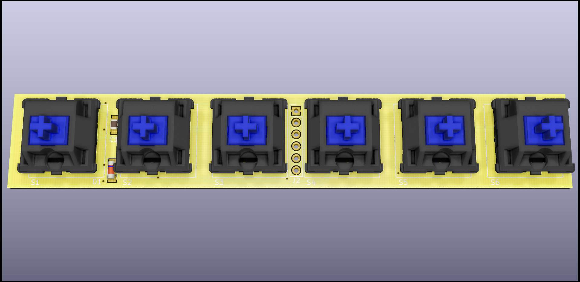
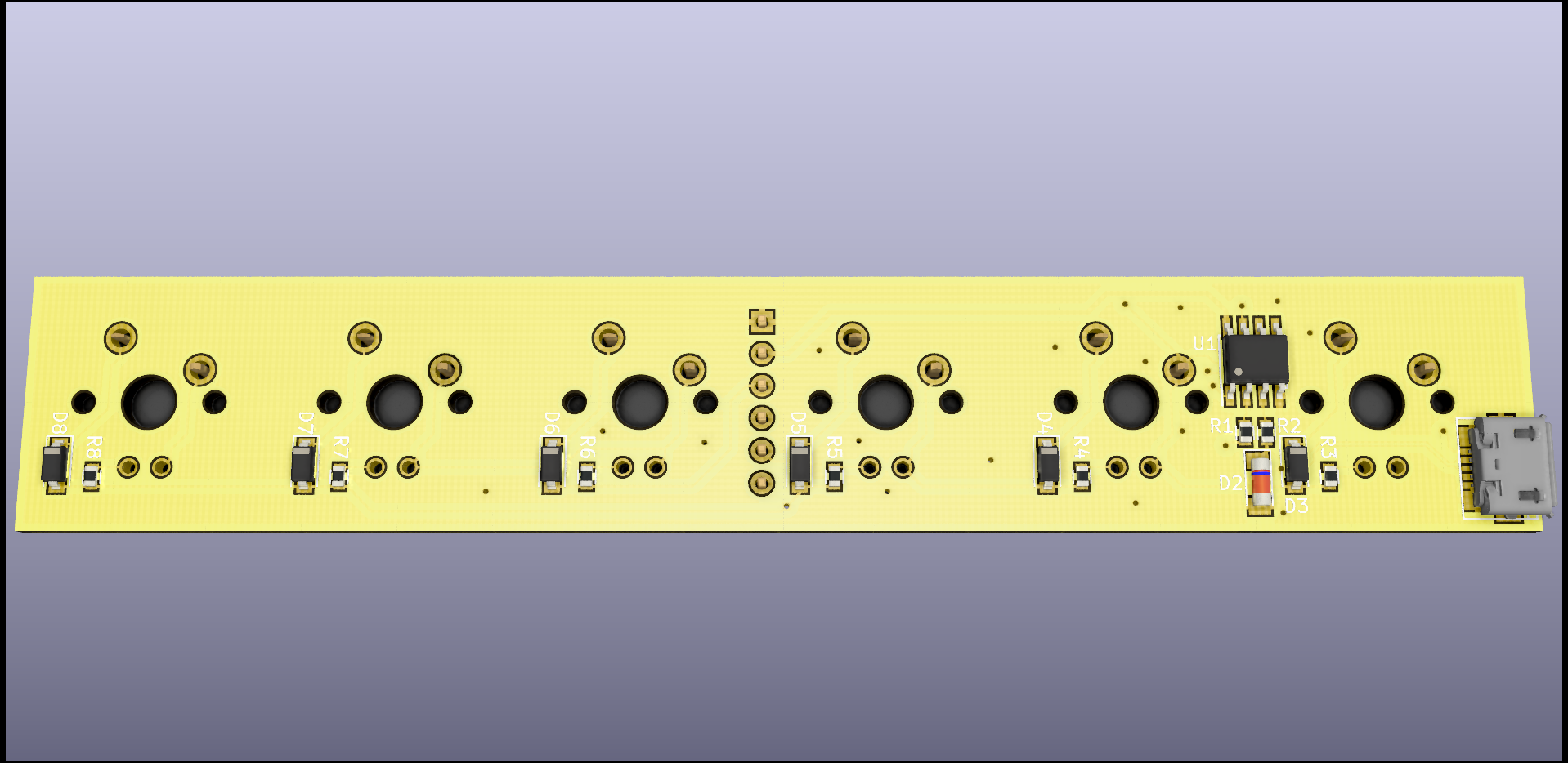
| Qty | Value | Footprint | References |
|---|---|---|---|
| 6 | 1n4148 | Diodes_SMD:D_SOD-123 | D3, D4, D5, D6, D7, D8 |
| 6 | 220R | Resistors_SMD:R_0603 | R3, R4, R5, R6, R7, R8 |
| 6 | MXALPS | CherryMX:Cherry-MX-RGB-LED | S1, S2, S3, S4, S5, S6 |
| 2 | 3v6 | Diodes_SMD:D_MiniMELF | D1, D2 |
| 2 | 68R | Resistors_SMD:R_0603 | R1, R2 |
| 1 | ATTINY85-20SU | Housings_SOIC:SOIC-8_3.9x4.9mm_Pitch1.27mm | U1 |
| 1 | C_Small | Capacitors_SMD:C_0805_HandSoldering | C1 |
| 1 | Conn_01x06 | Pin_Headers:Pin_Header_Straight_1x06_Pitch2.54mm | J2 |
| 1 | USB_B | Connectors:USB_Micro_B | J1 |
SensorsIot/SuperPower
Here you should find the best power supplies for your low-power projects

KivApple/dell-charger-emulator
Emulator of original Dell charger using ATTINY85


bwack/C64-Saver-bwack
C64 Saver v1 and v2 - Overvoltage protection for the C64 and its power brick.


valerionew/very-good-uc-doggos
A special graduation present for a special friend. Six microcontrollers in one devboard


spielhuus/LoRa-Environmental-Sensors
ATtiny85 based LoRa atmospheric sensor board with BME280
It measures 117 × 20 mm and has 2 copper layers, 1.6 mm thick.
26 parts, built around the ATTINY85-20SU. The full list of its parts is on this page, with links to each part's symbol and footprint where PCBKit's library has them.
From the Duckle29/WASD-keytester-pcb repository on GitHub, at the commit this page was made from: the board is WASD-key-tester.kicad_pcb. PCBKit opens the board in the browser, with nothing to install.
Its repository states no licence, so its author keeps all rights: ask Duckle29 before reusing the design.