
2 layers86 × 54 mm

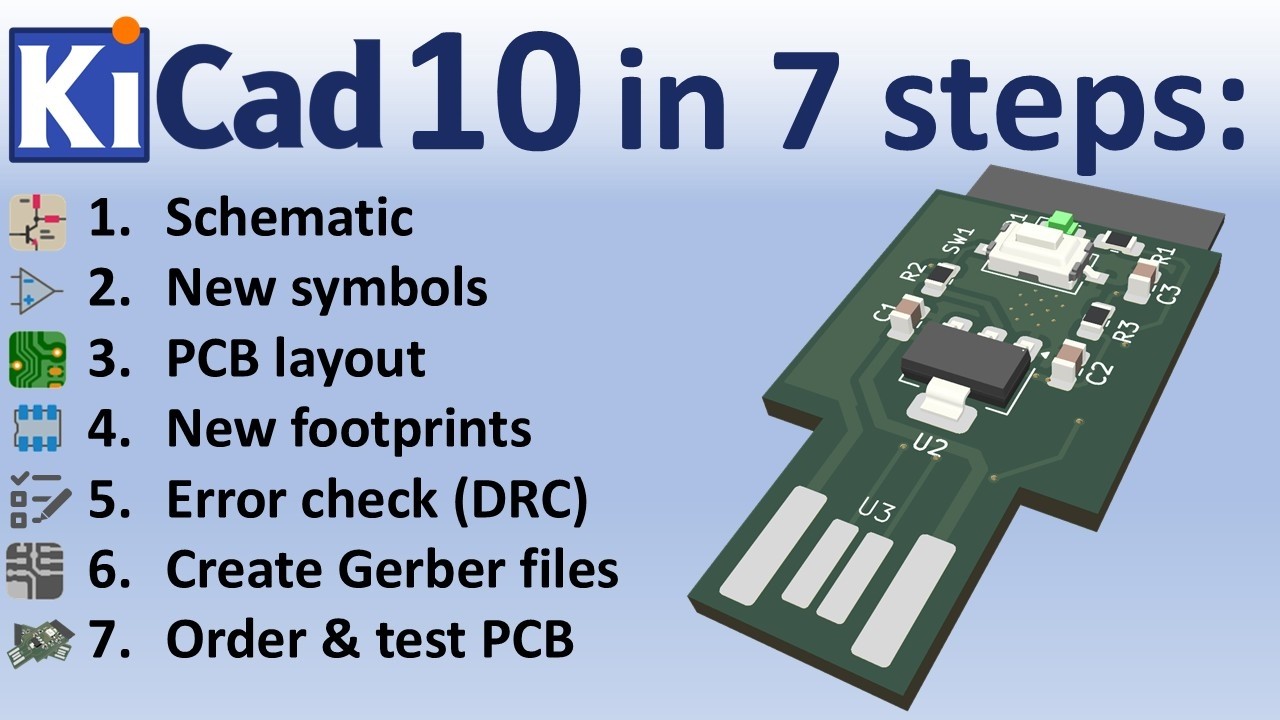
Master KiCad 10 in just 7 steps! In this tutorial, we design a custom, ultra-compact ESP32-S3 USB development board from scratch. From setting up your schematic to routing a 2-layer board with a custom PCB edge-connector, this video covers everything you need to know to get started with the latest features in KiCad 10.
ESP32 USB is an open-source printed circuit board by DesignGraveyard, from the DesignGraveyard/V002_KiCAD10_in_7_steps repository on GitHub, published under the MIT licence. It is a 2-layer board of 20.5 × 34.5 mm with 11 parts on 41 nets, routed with 104 tracks and 8 vias.
It is built around the ESP32-S3-WROOM-1-N8 and AMS1117-3.3. Its parts include 3 capacitors, 3 resistors, 3 ICs, 1 diode and 1 switch. It belongs with the microcontroller boards boards and the ESP32 boards of this library.


Master KiCad 10 in just 7 steps! In this video tutorial, I will show you how to design your own PCB in KiCAD10.
I will use a ESP32-S3 USB development board from a previous video as example and guide you through the design process in 7 steps:
Finally we will order, build & test the PCB.
You can order the PCB Directly at PCBWay:

For good contact the USB connector thickness is 2mm to 2.2mm, please check the instruction video and GitHub for the ESP32 "Bad USB" for more information.
| Qty | Value | Footprint | References |
|---|---|---|---|
| 2 | 10k | Resistor_SMD:R_0805_2012Metric_Pad1.20x1.40mm_HandSolder | R2, R3 |
| 2 | 10u | Capacitor_SMD:C_0805_2012Metric_Pad1.18x1.45mm_HandSolder | C1, C2 |
| 1 | 1k | Resistor_SMD:R_0805_2012Metric_Pad1.20x1.40mm_HandSolder | R1 |
| 1 | 1u | Capacitor_SMD:C_0805_2012Metric_Pad1.18x1.45mm_HandSolder | C3 |
| 1 | AMS1117-3.3 | Package_TO_SOT_SMD:SOT-223-3_TabPin2 | U1 |
| 1 | BOOT | Button_Switch_SMD:SW_Tactile_SPST_NO_Straight_CK_PTS636Sx25SMTRLFS | SW1 |
| 1 | ESP32-S3-WROOM-1 | RF_Module:ESP32-S3-WROOM-1 | U2 |
| 1 | LED | LED_SMD:LED_0805_2012Metric_Pad1.15x1.40mm_HandSolder | D1 |
| 1 | ~ | my_custom_footprints:USB_PCB_connector | U3 |


DevMubarak1/PidginTranslator
Handheld translator for Nigerian languages. No internet needed for common phrases, YarnGPT for everything else.


Tomas-Kuchta-FPV/Open-ESPilot
An open-source project to develop a custom ESP32-based flight controller designed primarily for use with ArduPilot. Focused on affordability, flexibility, and ease of integration with various robotic and UAV platforms.

RoboticsBrno/Robutek
Robůtek je robotická platforma založená na čipu ESP32-S3. Je velice rozšitiřelný, ale ze základu umí jezdit, kreslit fixou, jezdit po čáře, pohybovat se bludištěm. Programování je přes Jaculus.

romioRN/Dash6.8-hardware
wifi name "service", password 12345678, connect to 192.167.4.1

It measures 20.5 × 34.5 mm and has 2 copper layers, 1.6 mm thick.
11 parts, built around the ESP32-S3-WROOM-1-N8 and AMS1117-3.3. The full list of its parts is on this page, with links to each part's symbol and footprint where PCBKit's library has them.
From the DesignGraveyard/V002_KiCAD10_in_7_steps repository on GitHub, at the commit this page was made from: the board is ESP32_USB_KiCAD/ESP32_USB.kicad_pcb and its schematic ESP32_USB_KiCAD/ESP32_USB.kicad_sch. PCBKit opens the board in the browser, with nothing to install.
Its repository publishes it under the MIT licence: you may reuse it on that licence's terms (keep the author's notice, and for a copyleft licence share your changes alike).