4 layers75 × 60 mm
P1 rx
Deco025/resonare
Resonare: open-source 120 W LCC-S resonant wireless charger, transmitter and receiver boards (KiCad 10, 4-layer)
90 parts4CERN-OHL-S-2.0

 Deco025/resonare4
Resonare: open-source 120 W LCC-S resonant wireless charger, transmitter and receiver boards (KiCad 10, 4-layer)
P1 tx is an open-source printed circuit board by Deco025, from the Deco025/resonare repository on GitHub, published under the CERN-OHL-S-2.0 licence. It is a 4-layer board of 82 × 60 mm with 92 parts on 73 nets, routed with 336 tracks and 211 vias.
It is built around the UCC27211D, INA240A2D and BSC070N10NS3G, with the SS110 and SMAJ28A among its other parts. Its parts include 43 capacitors, 20 resistors, 7 ICs, 4 diodes and 4 transistors. It belongs with the STM32 boards of this library.


120 W LCC-S 谐振式无线充电:发射板 + 接收板


Resonare (Latin: “to resound”) is an open-source 120 W wireless charger built on an LCC-S resonant topology. A 24 V transmitter drives a full bridge into an LCC compensation network; the receiver rectifies, steps down with a synchronous buck and charges a supercapacitor bank through an ideal-diode stage. Both boards are 4-layer KiCad 10 designs with complete fabrication outputs.
| 发射板 TX(82 × 60 mm) | 接收板 RX(75 × 60 mm) |
|---|---|
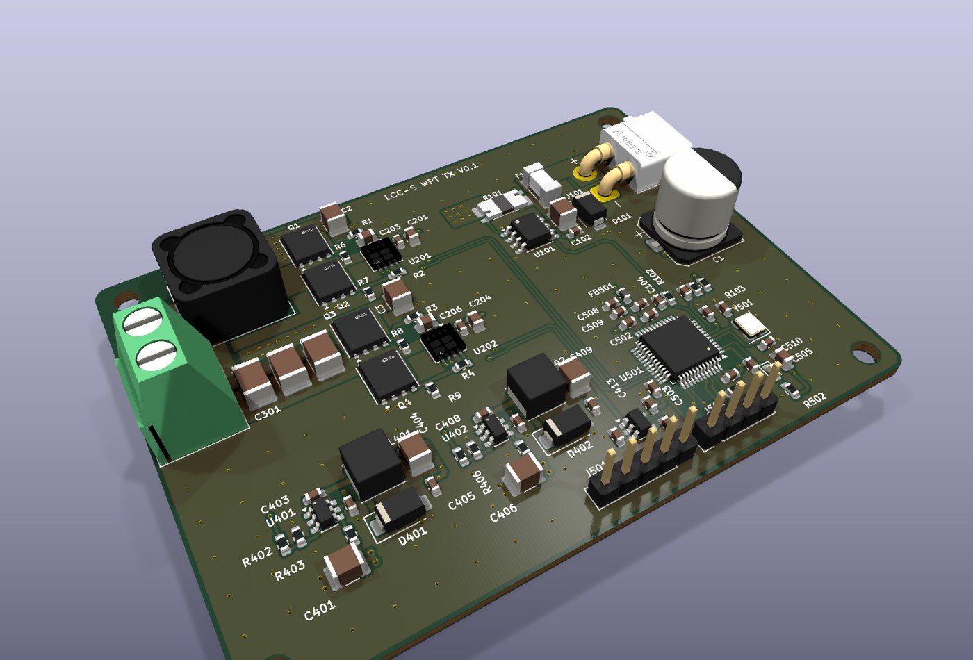 | 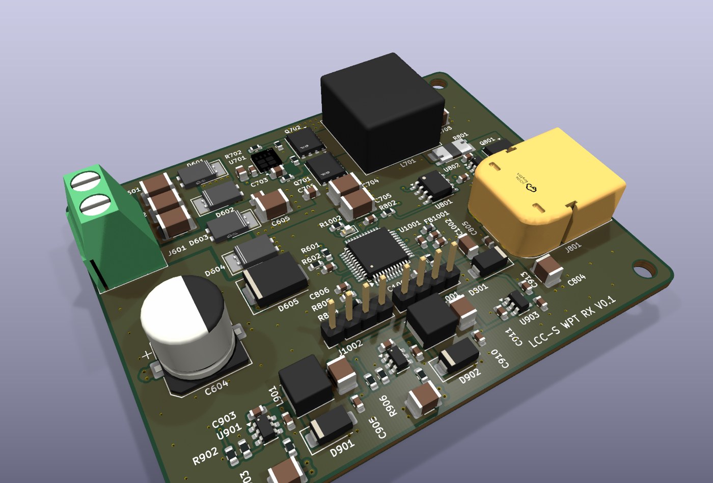 |
| 顶层 F.Cu | 底层 B.Cu(从背面看) | |
|---|---|---|
| 发射板 TX | 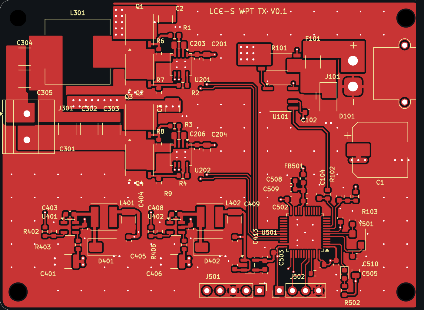 | 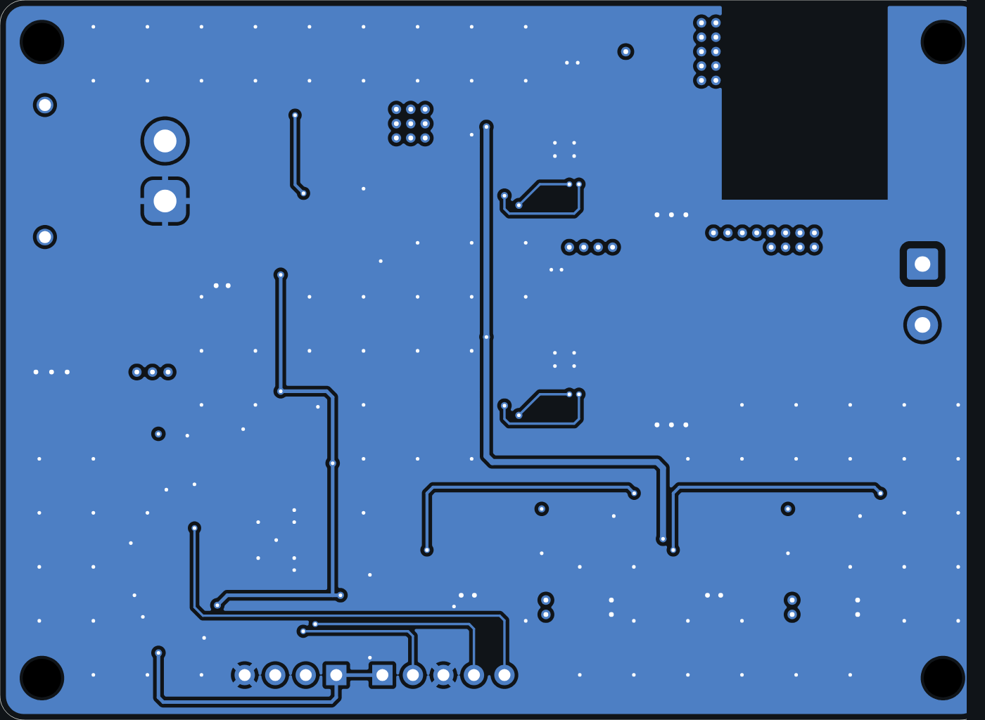 |
| 接收板 RX | 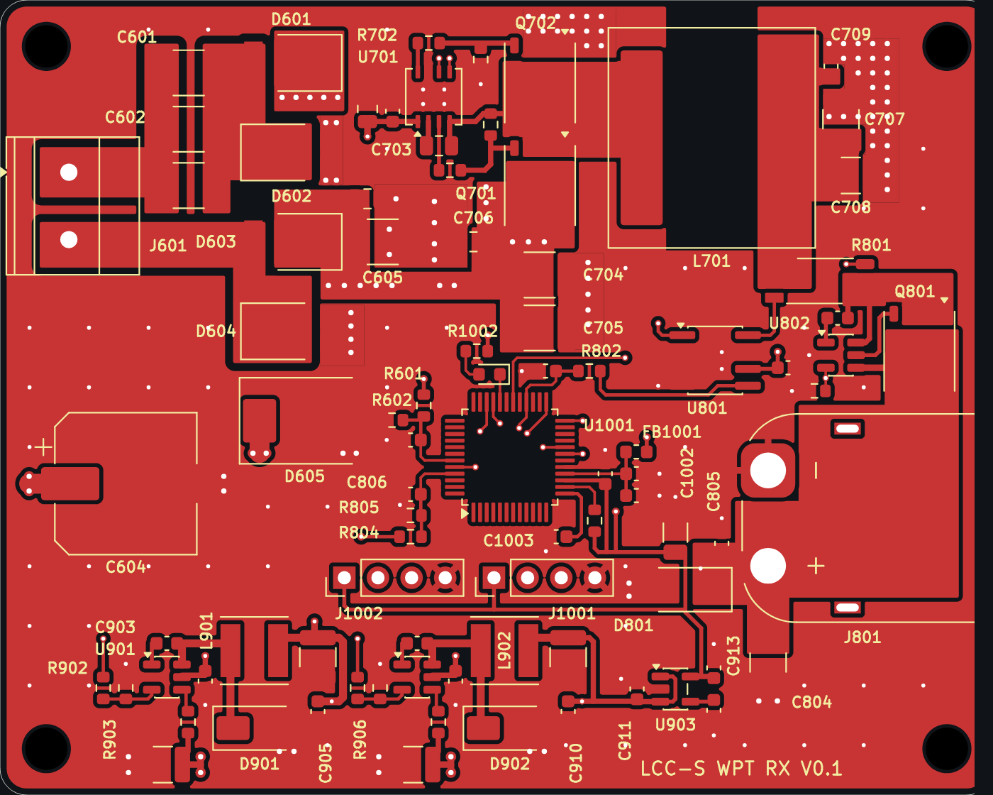 | 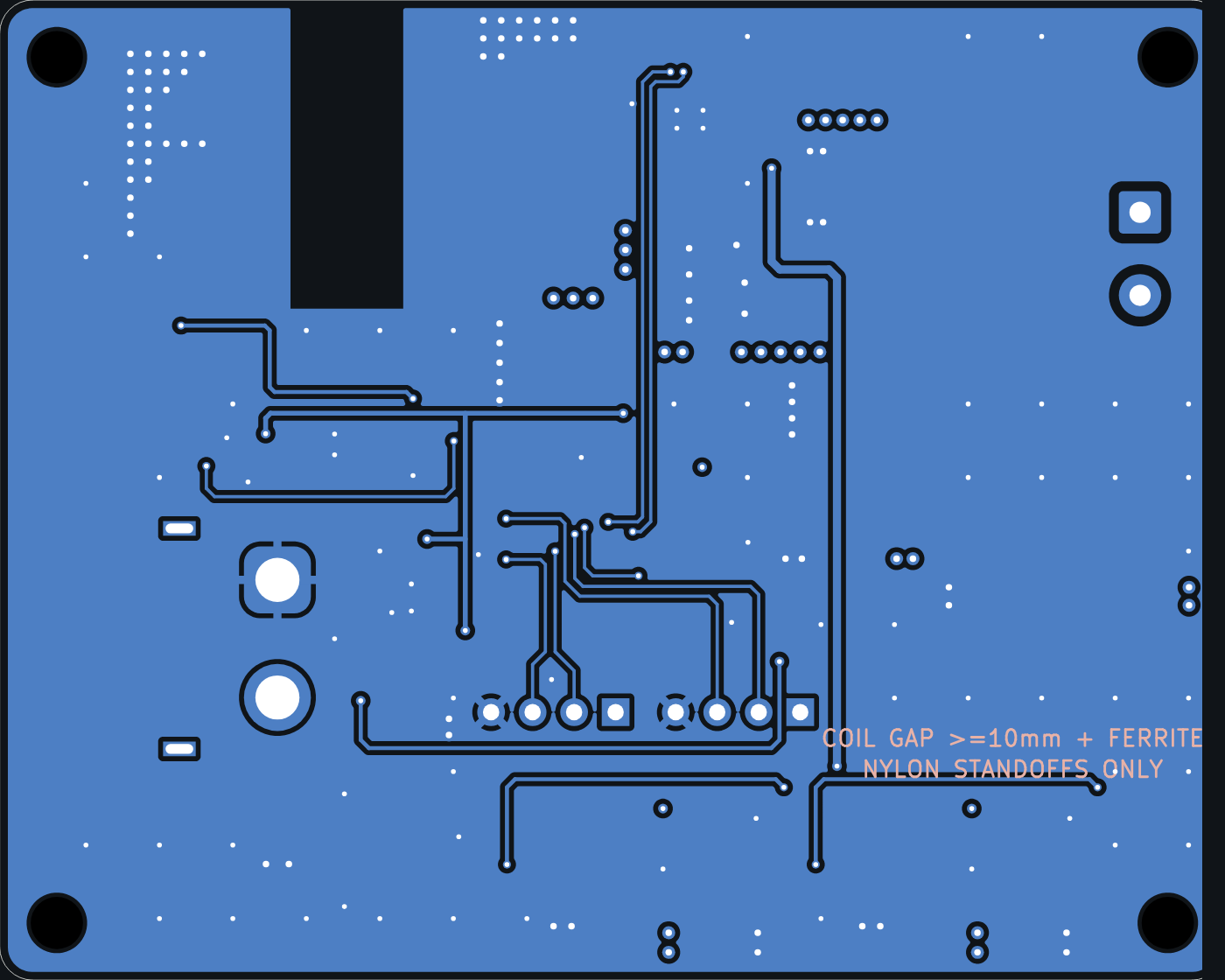 |
第 2 层为整层地、第 3 层为整层电源(TX:VBUS;RX:VRECT),图中只画出两个外层。
| 项 | 值 |
|---|---|
| 发射端输入 | 24 V DC,XT30 接口,输入平均电流约 5.9 A(按 85 % 效率估算) |
| 输出功率 | 120 W 级(超级电容端) |
| 拓扑 | 全桥逆变 + LCC-S 补偿 |
| 逆变 / 谐振频率 | 144 kHz |
| 补偿参数 | Lf 6 µH;Lt = Lr 20 µH;Cf ≈ 203.6 nF,Ct ≈ 87.3 nF,Cr ≈ 61.1 nF(理想调谐) |
| 整流母线 VRECT | 标称 30 V |
| 接收端降压 | 同步 Buck,200 kHz,15 µH;充电电流上限 10 A(峰值约 11.2 A) |
| 负载 | 超级电容组,6–24 V,等效 10 F,XT60 接口 |
| 电流采样 | 2 mΩ 四端分流电阻 + INA240A2(×50):10 A → 1.0 V |
| 主控 | TX:STM32G474CE(HRTIM 驱动全桥);RX:STC32G12K128(PWM 驱动 Buck) |
| PCB | 4 层,1.6 mm,外层 2 oz / 内层 1 oz |
flowchart LR
    subgraph TX [发射板]
        IN[24 V 输入<br/>保险丝 · TVS · 电流采样] --> FB[全桥<br/>4 × BSC070N10NS3G<br/>2 × UCC27211]
        FB --> LCC[LCC 补偿<br/>Lf · Cf · Ct]
        MCUT[STM32G474<br/>HRTIM · ADC · 比较器] --> FB
        AUXT[辅助电源<br/>24→12 V / 5 V / 3.3 V]
    end
    LCC -. 线圈 Lt ~ 磁耦合 ~ Lr .-> RECT
    subgraph RX [接收板]
        RECT[Cr + 全桥整流<br/>4 × SB2060L] --> BUCK[同步 Buck<br/>2 × BSC070N10NS3G<br/>UCC27211]
        BUCK --> OUT[电流采样 · 理想二极管<br/>LM74700 + N-MOS]
        OUT --> CAP[(超级电容组)]
        MCUR[STC32G12K128<br/>PWM · ADC · 比较器] --> BUCK
        AUXR[辅助电源<br/>VRECT→12 V / 5 V / 3.3 V]
endCHG_EN 控制。GND / GND_RX)。更完整的说明见 docs/design.md。
.
├── p1_tx/                 发射板 KiCad 工程(原理图 + PCB)
│   └── fab/               发射板生产文件(Gerber zip、BOM、坐标、装配图、DRC 报告)
├── p1_rx/                 接收板 KiCad 工程
│   └── fab/               接收板生产文件
├── p1/                    整机原理图(发射与接收在同一个工程里,作系统参考)
│   └── 3dmodels/          第三方 3D 模型的来源清单(模型文件不随仓库分发)
├── docs/
│   ├── design.md          设计说明
│   └── schematics/        原理图 PDF(不装 KiCad 也能看)
├── images/                3D 渲染图
├── CHANGELOG.md
└── LICENSE CERN-OHL-S-2.0p1_tx/p1_tx.kicad_pro(发射板)或 p1_rx/p1_rx.kicad_pro(接收板)。自定义符号在各工程自带的 p1_parts.kicad_sym 里;封装全部来自 KiCad 官方库。p1/3dmodels/,3D 查看器(Alt+3)里就能看到完整模型。不下载也不影响原理图、PCB 和生产文件。生产文件已经导出好,坐标原点在板的左上角:
下单要点:
DRC 里保留了几条已接受的丝印告警:驱动器封装的 1 脚标记压在自举电容焊盘上 0.05–0.14 mm;接线端子外框到达板边。这两种情况板厂都会自动裁掉焊盘上和板外的丝印。
详见 docs/design.md。
本项目的硬件设计文件(原理图、PCB、生产文件、文档)采用 CERN Open Hardware Licence Version 2 – Strongly Reciprocal (CERN-OHL-S-2.0)。
简单说:可以自由使用、学习、修改、生产和销售;但如果你发布修改后的设计,或者销售基于它的产品,必须用同样的许可证公开对应的设计源文件。
第三方封装、符号和 3D 模型各自遵循其原始许可,不在本许可证范围内。
欢迎通过 Issue 反馈问题或提出改进。
| Qty | Value | Footprint | References |
|---|---|---|---|
| 15 | 100nF | Capacitor_SMD:C_0603_1608Metric | C102, C105, C202, C205, C402, C403, C405, C407, C408, C410, C501, C502, C503, C504, C512 |
| 8 | 10k | Resistor_SMD:R_0603_1608Metric | R6, R7, R8, R9, R104, R403, R406, R501 |
| 4 | 10R | Resistor_SMD:R_0603_1608Metric | R1, R2, R3, R4 |
| 4 | 1uF | Capacitor_SMD:C_0603_1608Metric | C411, C413, C506, C508 |
| 4 | BSC070N10NS3G | Package_SON:Infineon_PG-TDSON-8_6.15x5.15mm | Q1, Q2, Q3, Q4 |
| 4 | M3 | MountingHole:MountingHole_3.2mm_M3 | H1, H2, H3, H4 |
| 3 | 10nF | Capacitor_SMD:C_0603_1608Metric | C412, C507, C509 |
| 3 | 10uF | Capacitor_SMD:C_1210_3225Metric | C101, C401, C406 |
| 2 | 100k | Resistor_SMD:R_0603_1608Metric | R401, R404 |
| 2 | 100nF | Capacitor_SMD:C_1812_4532Metric | C301, C302 |
| 2 | 15pF | Capacitor_SMD:C_0603_1608Metric | C510, C511 |
| 2 | 2.2uF | Capacitor_SMD:C_0805_2012Metric | C201, C204 |
| 2 | 220nF | Capacitor_SMD:C_0805_2012Metric | C203, C206 |
| 2 | 22uF | Capacitor_SMD:C_1210_3225Metric | C404, C409 |
| 2 | 4.7uF | Capacitor_SMD:C_1210_3225Metric | C2, C3 |
| 2 | LMR16006X | Package_TO_SOT_SMD:SOT-23-6 | U401, U402 |
| 2 | SS110 | Diode_SMD:D_SMA | D401, D402 |
| 2 | UCC27211 | Package_SON:HVSON-8-1EP_4x4mm_P0.8mm_EP2.2x3.1mm | U201, U202 |
| 1 | 100 | Resistor_SMD:R_0603_1608Metric | R102 |
| 1 | 10A | Fuse:Fuse_Littelfuse-NANO2-451_453 | F101 |
| 1 | 147k | Resistor_SMD:R_0603_1608Metric | R402 |
| 1 | 150k | Resistor_SMD:R_0603_1608Metric | R103 |
| 1 | 1k | Resistor_SMD:R_0603_1608Metric | R502 |
| 1 | 1nF | Capacitor_SMD:C_0603_1608Metric | C104 |
| 1 | 220uF | Capacitor_SMD:CP_Elec_10x10.5 | C1 |
| 1 | 2m | Resistor_SMD:R_Shunt_Vishay_WSK2512_6332Metric_T1.19mm | R101 |
| 1 | 3.3nF | Capacitor_SMD:C_1812_4532Metric | C303 |
| 1 | 33uH | Inductor_SMD:L_Taiyo-Yuden_NR-50xx | L402 |
| 1 | 4.7uF | Capacitor_SMD:C_0805_2012Metric | C505 |
| 1 | 47uH | Inductor_SMD:L_Taiyo-Yuden_NR-50xx | L401 |
| 1 | 5.6nF | Capacitor_SMD:C_1812_4532Metric | C305 |
| 1 | 54.9k | Resistor_SMD:R_0603_1608Metric | R405 |
| 1 | 600R@100MHz | Inductor_SMD:L_0603_1608Metric | FB501 |
| 1 | 6uH | Inductor_SMD:L_12x12mm_H8mm | L301 |
| 1 | 82nF | Capacitor_SMD:C_1812_4532Metric | C304 |
| 1 | 8MHz | Crystal:Crystal_SMD_3225-4Pin_3.2x2.5mm | Y501 |
| 1 | INA240A2D | Package_SO:SOIC-8_3.9x4.9mm_P1.27mm | U101 |
| 1 | LED_G | LED_SMD:LED_0603_1608Metric | D501 |
| 1 | SMAJ28A | Diode_SMD:D_SMA | D101 |
| 1 | STM32G474CETx | Package_QFP:LQFP-48_7x7mm_P0.5mm | U501 |
| 1 | SWD | Connector_PinHeader_2.54mm:PinHeader_1x05_P2.54mm_Vertical | J501 |
| 1 | TC2185-3.3 | Package_TO_SOT_SMD:SOT-23-5 | U403 |
| 1 | TX_COIL | TerminalBlock_Phoenix:TerminalBlock_Phoenix_MKDS-1,5-2-5.08_1x02_P5.08mm_Horizontal | J301 |
| 1 | UART | Connector_PinHeader_2.54mm:PinHeader_1x04_P2.54mm_Vertical | J502 |
| 1 | XT30_24V_IN | Connector_AMASS:AMASS_XT30PW-M_1x02_P2.50mm_Horizontal | J101 |
Deco025/resonare
Resonare: open-source 120 W LCC-S resonant wireless charger, transmitter and receiver boards (KiCad 10, 4-layer)


htsong-lab/hardware
Hardware engineering portfolio: FPGA high-speed board, RoboMaster power electronics and smart-car projects.

mobile-systems/psu48-ai
Проект импульсного блока питания PSU48-800 — БП 220 В AC → 48 В DC, 800 Вт(PFC + LLC)


BenjaminMeyerEE/Digital-Synchronous-Buck-Converter
12 V to 6 V, 10 A synchronous buck converter with closed-loop digital control on an STM32G474RET6. Custom 4-layer board in KiCad.

Blaze-Pascal/EKA-PiF-MCU_PSU
2-phase synchronous digitally controlled buck converter (30V in, up to 10A out). Features a 4-layer custom KiCad PCB optimized for EMI.
It measures 82 × 60 mm and has 4 copper layers, 1.6 mm thick.
92 parts, built around the UCC27211D, INA240A2D, BSC070N10NS3G and SS110. The full list of its parts is on this page, with links to each part's symbol and footprint where PCBKit's library has them.
From the Deco025/resonare repository on GitHub, at the commit this page was made from: the board is p1_tx/p1_tx.kicad_pcb and its schematic p1/p1.kicad_sch. PCBKit opens the board in the browser, with nothing to install.
Its repository publishes it under the CERN-OHL-S-2.0 licence: you may reuse it on that licence's terms (keep the author's notice, and for a copyleft licence share your changes alike).