4 layers77 × 48.6 mm
NX ISD
Ghost3379/NX-ISD
A more sophisticated version of the Artemis Watch by Circuitmess.
116 parts2GPL-3.0

 CopperPilot/CM5-AI-Cam-CopperPilot
A Raspberry Pi Compute Module 5 carrier for edge AI vision, in the CM5's own 55 × 40 mm footprint. 100 Ω MIPI and HDMI pairs, 90 Ω USB.
CM5-AI Cam CopperPilot is an open-source printed circuit board by CopperPilot, from the CopperPilot/CM5-AI-Cam-CopperPilot repository on GitHub. It is a 6-layer board of 55 × 40 mm with 90 parts on 118 nets, routed with 1,755 tracks and 322 vias.
It is built around the MP1658GTF-Z, FSUSB42UMX and RT9013-12GB, with the RT9193-18GB, RT9193-28GB and DMG1012T among its other parts. Its parts include 31 capacitors, 29 resistors, 8 ICs, 6 inductors and 2 transistors. It belongs with the computers and single-board computers and interfaces and adapters boards and the Raspberry Pi (Linux) boards of this library.







An ultra-compact, high-density, 6-layer carrier board designed for the Raspberry Pi Compute Module 5 (CM5), purpose-built for embedded computer vision, edge AI inference, autonomous robotics, and smart camera applications. Engineered in an exact 55.0 mm × 40.0 mm form factor matching the CM5 module dimensions, the board provides dedicated low-noise power rails, controlled-impedance differential routing (100 Ω for MIPI and HDMI, 90 Ω for USB), onboard common-mode filtering, high-speed peripheral multiplexing, and standard 40-pin Raspberry Pi GPIO expansion.
| Top Isometric View | Bottom Mezzanine View |
|---|---|
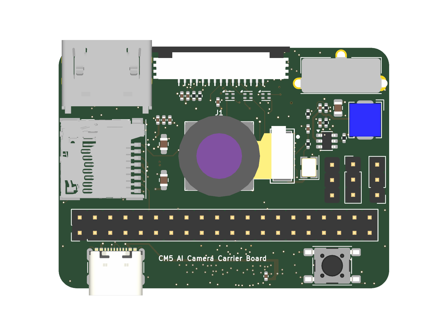 | 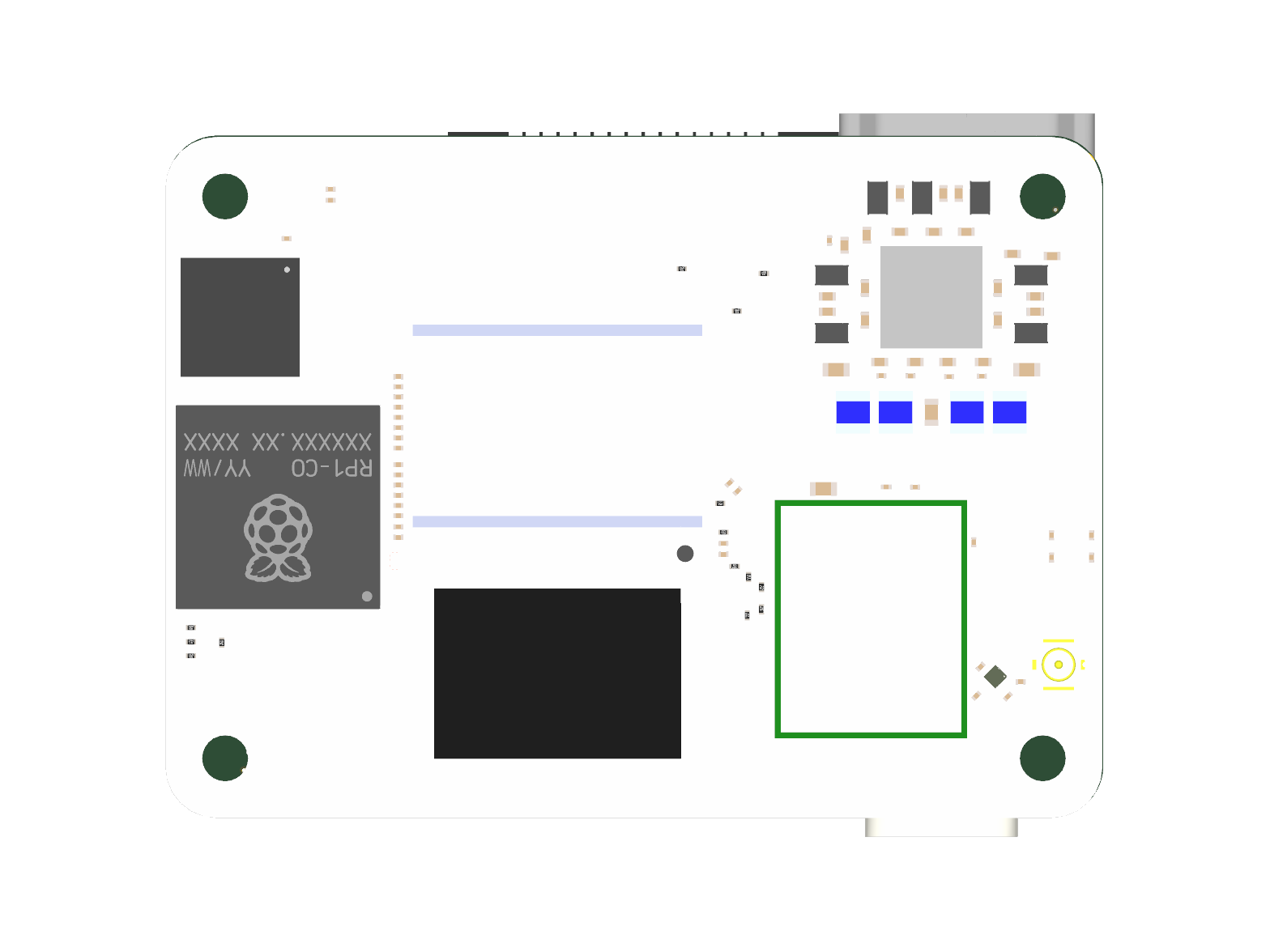 |
| Full System Isometric | Top Routing (F.Cu) |
|---|---|
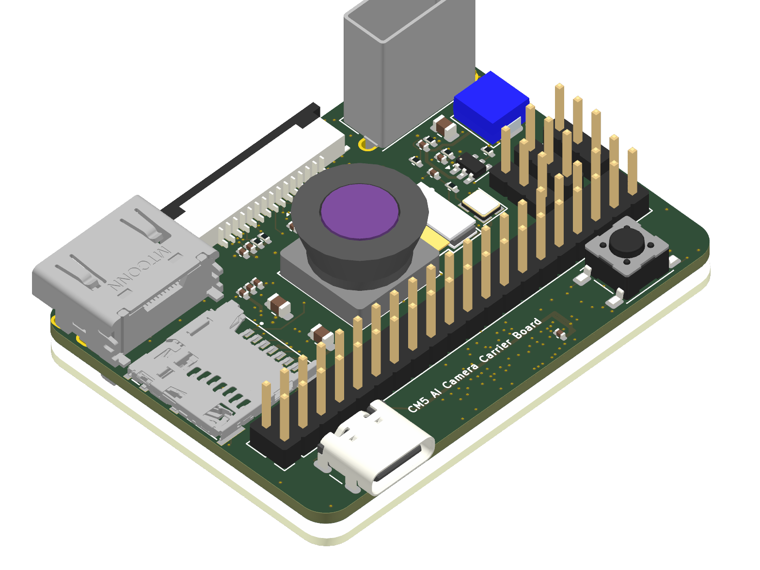 | 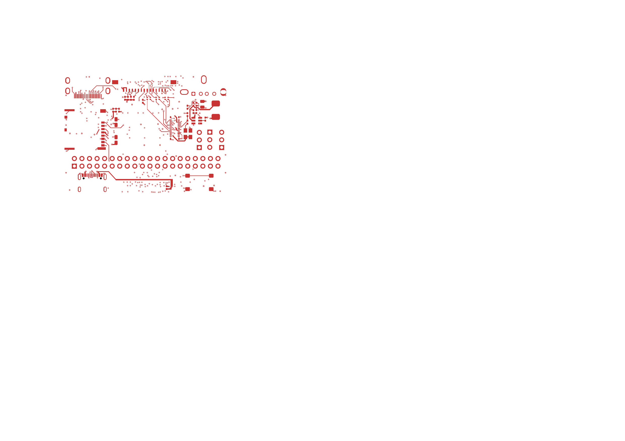 |
                    +-------------------------------------------------------+
                    |                      Power Entry                      |
                    | USB-C (Type_C1) w/ 5.1k CC (R2, R3) OR 40-Pin PI1 Header
                    |                             |                         |
                    |               MPS MP1658 3.3V / 3A Buck (U5)          |
                    |                             |                         |
                    |     +-----------------------+-------------------+     |
                    |     |                       |                   |     |
                    | RT9193-2.8V (U1)    RT9193-1.8V (U2)    RT9013-1.2V (U3)
                    +-----+-----------------------+-------------------+-----+
                          |                       |                   |
                     CAM_2V8 Rail            CAM_1V8 Rail        CAM_1V2 Rail
                          |                       |                   |
+-------------------------v-----------------------v-------------------v-----+
|                         Camera Imaging Subsystem                          |
| 30-Pin Sony IMX219 Autofocus Camera Connector (J1)                        |
| 3x 1210 High-Frequency Common-Mode Chokes (L1, L2, L3)                    |
| 2-Lane MIPI CSI-2 (100 Ω Differential, HighSpeed_100R, 0.127 mm Width)    |
+---------------------------------------------+-----------------------------+
                                              |
                          Mezzanine DF40C     | MIPI CSI-2 (100 Ω Diff)
                          Mezzanine DF40C     | (High-Speed Imaging)
+---------------------------------------------v-----------------------------+
| Raspberry Pi Compute Module 5 (Module1) |This design was developed using the architecture and schematic concepts of the Waveshare CM4 / CM5 Nano Base Board (C) as an engineering reference. Our team conducted a thorough hardware design review and implemented major electrical, signal integrity, DFM, and manufacturing improvements to deliver a validated, production-ready edge AI camera carrier.
| Domain | Baseline Reference Limitation | Implemented Engineering Improvement | Benefit / Impact |
|---|---|---|---|
| Power Regulation | Faulty feedback divider and mismatched LCSC part (C25916 6.49 kΩ) on 3.3V buck regulator U5 (MP1658GTF-Z, C2960187); C21 snubber capacitor assigned 12 pF (C1547). | Configured feedback divider with precision 61.9 kΩ ±1% (R20, C25803) and 20.0 kΩ ±1% (R21, C25765) resistors for exact 3.305 V output ($V_{REF}=0.807\text{ V}$); verified 0.1 µF bootstrap (C24) and 10 Ω + 330 pF (R16 + C21, C1534) SW snubber. | Eliminates catastrophic overvoltage/undervoltage risk on /PWR_3V3 and damps high-frequency switching ring. |
| Camera Power & Clock | U3 1.2V camera core LDO assigned a 3.3V LCSC part (C7434207); U1 2.8V LDO assigned an invalid LCSC code; C20 on 24 MHz /MCLK set to 0.1 µF (fc = 72.3 kHz), attenuating the sensor clock. | Assigned verified Richtek LDOs (U1 2.8V C15075, U2 1.8V C27416, U3 1.2V C47773) and restored C20 to 10 pF (C32949) with R10 = 22 Ω (fc = 723 MHz). | Protects the 1.2V Sony IMX219 core from 3.3V overvoltage and preserves clean 24 MHz CMOS clock integrity. |
Differential Impedance (100 Ω vs 90 Ω) | Unassigned netclasses in .kicad_pro (netclass_patterns: []) and documentation conflating MIPI CSI-2, DSI, HDMI TMDS, and USB into a single 90 Ω class with 0.150 mm default trace widths. | Separated and assigned HighSpeed_100R (100 Ω for MIPI CSI-2, MIPI DSI, and HDMI TMDS: W = 0.127 mm, S = 0.150 mm) and HighSpeed_90R (90 Ω for USB 2.0: W = 0.180 mm, S = 0.150 mm) across .kicad_pro, .kicad_pcb, and .kicad_dru. | Matches official Raspberry Pi CM5/CM4, MIPI D-PHY, HDMI 1.4b/2.0 (100 Ω), and USB 2.0 Hi-Speed (90 Ω) specifications on JLCPCB's impedance calculator. |
| USB Architecture | Package suffix mismatch on U6 (FSUSB42MX MSOP-10 vs FSUSB42UMX UQFN-10) and unverified VBUS switch documentation. | Standardized U6 to FSUSB42UMX (C11145, UQFN-10_1.4x1.8mm_P0.4mm) with STMPS2171STR (U8) providing dedicated 5V load switching for USB-A host port J2. | Enables reliable USB 2.0 routing between USB-C (rpiboot device mode) and vertical USB-A host peripheral port. |
| Display Connector Parity | DSI1 15-pin FPC connector symbol included legacy unrouted pin SH with no matching pad name on footprint Molex_200528-0150. | Synchronized CM5:DSI_15P symbol with the 15-circuit footprint so kicad-cli pcb drc --schematic-parity passes with zero net conflicts. | Eliminates schematic-to-PCB netlist parity errors. |
| DFM & Custom Rules | Custom DRC rules in .kicad_dru lacked explicit Decision ID traceability and controlled-impedance width constraints. | Annotated all custom rules (DEC-001 through DEC-005) and added explicit HighSpeed_100R_Impedance_Width (0.127 mm) and HighSpeed_90R_Impedance_Width (0.180 mm) DRC constraints. | Enforces trace width and clearance compliance automatically during kicad-cli pcb drc. |
| Turnkey PCBA Sourcing | DNP strap resistors (R31, R32, R33 for WL_nDisable, BT_nDisable, USB_OTG_ID) erroneously included in BOM/CPL; mismatched LCSC codes on HDMI1 and L1–L3. | Excluded DNP straps R31–R33 (--exclude-dnp) so Wi-Fi/Bluetooth stay enabled; assigned verified LCSC parts for HDMI1 (C424662) and 1.2×1.0 mm chokes L1–L3 (C110443); consolidated 0.1uF (C1525) BOM rows. | Ready for automated turnkey fabrication and double-sided SMT assembly (87 populated parts across 42 BOM lines). |
| Automated Testing | No automated verification of differential netclasses, controlled-impedance trace widths, or critical BOM LCSC mappings. | Expanded the automated PyTest verification suite (tests/test_pcb.py) to 29 assertion tests alongside the 11-stage acceptance runner (review/verify.sh). | Continuously verifies physical dimensions, stackup, 100 Ω / 90 Ω differential netclasses and trace widths, DRC/ERC parity, and BOM/CPL integrity. |
Module1, C597931) with 0.40 mm pitch providing high-speed interconnects for MIPI CSI-2, MIPI DSI, HDMI TMDS, USB 2.0, SDIO, and GPIO.Type_C1, GCT USB4105-GF-A, C3020560) or via 40-pin GPIO expansion header (PI1). Recommended power supply: 5V / 3A minimum.R2, R3, C25905) for standard 5V/3A USB Type-C source negotiation./PWR_3V3): Monolithic Power Systems MP1658GTF-Z synchronous buck converter (U5, SOT-563, C2960187) delivering up to 3.0 A continuous output current (R20 = 61.9 kΩ C25803, R21 = 20.0 kΩ C25765 for 3.305 V nominal output), filtered by a 4.7 µH shielded power inductor (L7, C840574) and dual 22 µF 0805 ceramic output capacitors (C25, C26).CAM_2V8 (/2V8): 2.8 V analog rail via Richtek RT9193-28GB LDO (U1, C15075) with ferrite bead input filter (FB1, 120 Ω C50843).CAM_1V8 (/1V8): 1.8 V digital I/O and oscillator rail via Richtek RT9193-18GB LDO (U2, C27416).CAM_1V2 (/1V2): 1.2 V core logic rail via Richtek RT9013-12 LDO (U3, C47773).J1, Hirose DF37NB-30DS-0.4V(75), C6539772) designed for Sony IMX219-D160 camera modules.L1, L2, L3, MCF1210BF2-900T01, C110443) placed on MIPI CSI-2 clock and data lanes for high-frequency common-mode noise suppression.HighSpeed_100R, W = 0.127 mm, S = 0.150 mm) on MIPI CSI-2 lanes (/CAM0_* and /CSI_*).X1, 3.2 × 2.5 mm, C717686) with 22 Ω series damping resistor (R10) and 10 pF edge-rate filter capacitor (C20, C32949, $f_c = 723\text{ MHz}$).HDMI1, C424662) with dedicated 5 V power distribution switch (U4, STMPS2171STR, C157437), hot-plug detection, and controlled 100 Ω differential impedance (HighSpeed_100R, W = 0.127 mm, S = 0.150 mm) on TMDS clock and data pairs (/HDMI0_CLK_P/N, /HDMI0_TX0..2_P/N).DSI1, C2914074) powered from /PWR_3V3 with controlled 100 Ω differential impedance (HighSpeed_100R, W = 0.127 mm, S = 0.150 mm) on DSI clock and data lanes (/DSI1_CLK_P/N, /DSI1_D0..1_P/N).TF1, C91145) with dedicated STMPS2171STR 3.3 V load switch (U7, C157437) controlled by /SD_PWREN.J2, Molex 67298-4090, C698207) with STMPS2171STR 5 V VBUS switch (U8, C157437) and USB Type-C peripheral port (Type_C1) multiplexed through an onsemi FSUSB42UMX high-speed USB 2.0 switch (U6, C11145), routed at controlled 90 Ω differential impedance (HighSpeed_90R, W = 0.180 mm, S = 0.150 mm).Key1, C318884) connected to GPIO21 with a 10 kΩ pull-up (R11) to /PWR_3V3.L5, C2286) and Green Activity LED (L6, C72043).Module1) on the bottom side (B.Cu).Type_C1. The onboard CC termination resistors (R2, R3) negotiate standard 5V operation from USB Power Delivery sources.5V) and Pin 6 (GND) of the 40-pin header (PI1). Do not connect an external 5V supply to PI1 simultaneously with a host PC on Type_C1.L5) illuminates immediately when the regulated 3.3V system rail (/PWR_3V3) is active.For CM5 modules equipped with onboard eMMC:
/PI_BOOT (H4 Pin 1) and /USB_SEL (H4 Pin 3) low to GND (H4 Pin 2) so the BCM2712 processor enters USB rpiboot mode and the FSUSB42UMX multiplexer (U6) selects the USB Type-C port (Type_C1).Type_C1) and run rpiboot:
rpibootJ1./boot/firmware/config.txt:
# Enable Sony IMX219 Camera Sensor
dtoverlay=imx219rpicam-apps:
rpicam-hello --list-cameras
rpicam-hello -t 5000HDMI1): Plug a standard Mini-HDMI to HDMI cable into HDMI1. Video output is automatically detected via EDID / HPD.DSI1): Connect a 15-pin 1.0 mm pitch DSI display ribbon cable to DSI1 and enable the matching DSI overlay in /boot/firmware/config.txt (e.g., dtoverlay=vc4-kms-dsi-7inch).Key1) is wired to GPIO21 with a 10 kΩ pull-up (R11) to /PWR_3V3. Pressing the button pulls GPIO21 low.PI1) follows the standard Raspberry Pi 40-pin pinout.The board .kicad_pcb stackup is synchronized with the JLCPCB JLC06161H-7628 6-layer controlled-impedance stackup (1.6 mm nominal thickness, with cross-compatibility verified against JLC06161H-3313):
| Layer | Type | Copper Weight | Thickness | Physical Allocation in .kicad_pcb |
|---|---|---|---|---|
| 1. F.Cu | Signal | 1.0 oz (35 µm) | 0.0350 mm | Top SMT components, high-speed microstrip escapes, camera chokes (L1–L3), buck converter (U5) |
| Dielectric 1 | Prepreg (7628) | — | 0.2104 mm | FR-4 ($\varepsilon_r = 4.6$; 0.0994 mm $\varepsilon_r = 4.05$ on JLC06161H-3313) |
| 2. In1.Cu | Plane / Signal | 0.5 oz (15.2 µm) | 0.0152 mm | Primary GND reference plane (zone GND) and inner escape routing |
| Dielectric 2 | Core | — | 0.4000 mm | FR-4 Core ($\varepsilon_r = 4.6$; 0.5500 mm on JLC06161H-3313) |
| 3. In2.Cu | Signal | 0.5 oz (15.2 µm) | 0.0152 mm | Inner high-speed signal routing (HDMI0, DSI1, peripheral signals) |
| Dielectric 3 | Prepreg (7628) | — | 0.2104 mm | FR-4 ($\varepsilon_r = 4.6$; 0.0994 mm $\varepsilon_r = 4.05$ on JLC06161H-3313) |
| 4. In3.Cu | Power / Signal | 0.5 oz (15.2 µm) | 0.0152 mm | Internal power distribution zones (/PWR_3V3, /CM5_5V) and inner signal routing |
| Dielectric 4 | Core | — | 0.4000 mm | FR-4 Core ($\varepsilon_r = 4.6$; 0.5500 mm on JLC06161H-3313) |
| 5. In4.Cu | Plane / Signal | 0.5 oz (15.2 µm) | 0.0152 mm | Secondary GND reference plane (zone GND) and high-speed routing |
| Dielectric 5 | Prepreg (7628) | — | 0.2104 mm | FR-4 ($\varepsilon_r = 4.6$; 0.0994 mm $\varepsilon_r = 4.05$ on JLC06161H-3313) |
| 6. B.Cu | Signal | 1.0 oz (35 µm) | 0.0350 mm | Bottom mezzanine (Module1), camera LDOs (U1–U3), USB mux (U6), power switches (U4, U7, U8) |
The project .kicad_pro and .kicad_dru files separate differential pairs into two dedicated controlled-impedance netclasses verified against JLCPCB's controlled-impedance models:
Netclass (CM5-AI-Cam-CopperPilot.kicad_pro) | Target Impedance | Assigned Interfaces & Nets | Routed Trace Width ($W$) | Differential Gap ($S$) | Calculated $Z_{\text{diff}}$ / $Z_0$ (JLC06161H-7628 Stripline) | Calculated $Z_{\text{diff}}$ / $Z_0$ (JLC06161H-3313 Microstrip) |
|---|---|---|---|---|---|---|
HighSpeed_100R | 100 Ω ±10% Diff | MIPI CSI-2 (/CAM0_*, /CSI_*), MIPI DSI (/DSI1_*), HDMI TMDS (/HDMI0_CLK_*, /HDMI0_TX*) | 0.127 mm (5.0 mil) | 0.150 mm (5.9 mil) | 100.1 Ω | 98.3 Ω |
HighSpeed_90R | 90 Ω ±10% Diff | USB 2.0 Hi-Speed (/USB0_P/N, /USB0_B_P/N, /USBB_P/N, /USBD0_P/N) | 0.180 mm (7.1 mil) | 0.150 mm (5.9 mil) | 89.6 Ω | 88.7 Ω |
| Single-Ended Clocks / SDIO | 50 Ω ±10% SE | Camera & SDIO Clocks (/MCLK, /X1_OUT, /SD_CLK, /SD_CMD, /SD_DAT0..3) | 0.180 mm (7.1 mil) | — | 53.7 Ω | 47.0 Ω |
Power | Low-Z Distribution | /CM5_5V, /PWR_3V3, /CM5_3V3, /CM5_1V8, /HDMI_5V, /USB_5V, /SD_3.3V, /2V8, /1V8, /1V2 | 0.150–0.500 mm (0.35 mm nom) | — | — | — |
Default | General I/O | GPIO, I2C, control and status signals | 0.150 mm | — | — | — |
HighSpeed_100R), minimum global clearance 0.095 mm, via drill 0.20 mm / pad 0.40 mm (hole-to-hole spacing ≥ 0.254 mm, with local 0.070 mm via-to-via pad clearance rule DEC-003 under the 0.40 mm pitch Hirose DF40 mezzanine)..
├── Makefile # Unified build orchestrator (test, lint, drc, erc, fab)
├── .gitignore # Clean Git exclusion specification
├── LICENSE # CERN Open Hardware Licence v2 - Strongly Reciprocal
├── README.md # Comprehensive hardware specifications & documentation
├── CM5-AI-Cam-CopperPilot.kicad_pro# KiCad 10 project definition & 100R/90R net classes
├── CM5-AI-Cam-CopperPilot.kicad_sch# Complete multi-block schematic capture
├── CM5-AI-Cam-CopperPilot.kicad_pcb# 6-layer PCB layout (100% routed, 0 DRC violations)
├── CM5-AI-Cam-CopperPilot.kicad_dru# Custom design rules & impedance width constraints
├── CM5.kicad_sym # Project-local schematic symbol library
├── sym-lib-table # Project symbol library registry (${KIPRJMOD})
├── fp-lib-table # Project footprint library registry (${KIPRJMOD})
├── CM5.pretty/ # Self-contained project-local footprint library
├── CM5.3dshapes/ # 3D mechanical models (STEP/WRL)
├── 3dmodels/ # Mezzanine reference CAD models
├── docs/ # Documentation assets and renders
│ └── images/ # 3D renders, layer graphics, and mechanical diagrams
├── tests/ # Automated 29-point PyTest hardware verification suite
│ ├── conftest.py # S-expression AST parsers & KiCad CLI fixtures
│ └── test_pcb.py # 29 automated hardware assertion tests
├── review/ # Formal review deliverable & visual diff collateral
│ ├── index.html # Interactive visual review report & issue cards
│ ├── verify.sh # Automated acceptance test runner (T1 - T11)
│ ├── issues.json # Machine-readable issue register (all verified)The repository includes a multi-tiered test infrastructure running both unit-level hardware property assertions and full-design acceptance validations.
# Run the complete test and linting pipeline
make all

# Run the 29-point automated PyTest hardware test suite
make test

# Run KiCad Electrical Rule Check (ERC) and Design Rule Check (DRC)
make erc
make drc

# Run the full 11-stage hardware acceptance test runner
make verify

# Rebuild the interactive visual review report
make report

# Generate and package production Gerbers, drill files, BOM, and CPL
make fabtests/test_pcb.py)| Test Group | Test Case | Target / Specification | Result |
|---|---|---|---|
| Board Physical | test_board_dimensions | 55.0 mm × 40.0 mm (±0.5 mm tolerance) | PASS |
test_board_outline_closed | Continuous closed Edge.Cuts boundary with rounded corners | PASS | |
test_layer_stackup_6layer | 6 copper layers (F.Cu, In1-4.Cu, B.Cu) with JLC06161H-7628 dielectrics | PASS | |
test_board_thickness_nominal | Nominal board thickness of 1.6 mm | PASS | |
| Connectivity & Parity | test_drc_zero_errors | KiCad CLI DRC: 0 errors, 0 warnings | PASS |
test_drc_zero_unconnected_items | 100% routed copper (0 unconnected airwires) | PASS | |
test_drc_schematic_parity | Zero netlist or component parity mismatches | PASS | |
test_erc_zero_errors_and_warnings | KiCad CLI ERC: 0 errors, 0 warnings | PASS | |
test_power_distribution_nets_present | GND, 5V, 3V3 power distribution nets verified | PASS | |
test_camera_subsystem_nets_present | Dedicated camera rails (/2V8, /1V8, /1V2) & MIPI CSI-2 nets verified | PASS | |
test_usb_differential_nets_present | High-speed USB differential pairs verified | PASS | |
| Impedance, Trace Geometry & DFM | test_differential_netclasses_configured | HighSpeed_100R (100 Ω MIPI/HDMI) and HighSpeed_90R (90 Ω USB) assigned in .kicad_pro | PASS |
test_mipi_hdmi_100ohm_trace_widths | All 26 MIPI CSI-2, DSI, and HDMI differential nets routed at 0.127 mm (100 Ω) | PASS | |
test_usb_90ohm_trace_widths | All 8 USB 2.0 differential nets routed at 0.180 mm (90 Ω) | PASS | |
test_signal_trace_min_width | Trace width ≥ 0.09 mm (JLCPCB 6-layer capability) | PASS | |
test_power_trace_widths | Power trace width ≥ 0.15 mm (low impedance) | PASS | |
test_via_drill_and_pad_dimensions | Via drill ≥ 0.20 mm, pad diameter ≥ 0.40 mm | PASS | |
test_via_annular_rings | Via annular rings ≥ 0.10 mm | PASS | |
| Subsystem Circuits | test_cm5_module_footprint_present | Hirose DF40 100-pin mezzanine footprint verified | PASS |
test_camera_subsystem_chokes | Common-mode chokes L1, L2, L3 populated (C110443) | PASS | |
test_camera_ldos_present | Dedicated camera LDOs U1 (C15075), U2 (C27416), U3 (C47773) populated | PASS | |
test_buck_regulator_present | MP1658 3.3V/3A synchronous buck regulator U5 populated (C2960187) | PASS | |
test_usb_c_cc_termination_resistors | 5.1 kΩ pull-down resistors R2, R3 on CC pins | PASS | |
test_peripherals_present | Connectors HDMI1, DSI1, TF1, PI1, Type_C1, J2 verified | PASS | |
| Repo Hygiene & DFM | test_no_absolute_user_paths_in_tables | Zero user machine path leaks; 100% relative ${KIPRJMOD} paths | PASS |
test_manufacturing_bom_completeness | BOM complete with 100% verified LCSC part numbers | PASS | |
test_critical_bom_lcsc_and_dnp_exclusion | Verified LCSC codes on R20, U1, U3, U5, U6, HDMI1, L1–L3, C20, C21 & DNP exclusion of R31–R33 | PASS | |
test_manufacturing_cpl_completeness | CPL centroid coordinates, rotations, and DNP exclusion verified | PASS | |
test_gerber_package_files | All 6 copper layers, mask, silk, paste, and drill files present | PASS |
An interactive, self-contained HTML review deliverable is available at review/index.html.
Key features of the report:
To order fabricated and assembled boards directly from JLCPCB:
jlcpcb_production/gerbers_jlcpcb.zip.jlcpcb_production/assembly/bom_jlcpcb.csv.jlcpcb_production/assembly/cpl_jlcpcb.csv.manufacturing/ORDER_SPEC.md for full order form field values.This project is licensed under the CERN Open Hardware Licence Version 2 - Strongly Reciprocal (CERN-OHL-S-2.0).
| Qty | Value | Footprint | References |
|---|---|---|---|
| 12 | 0.1uF | CM5:C_0402_1005Metric | C3, C10, C14, C17, C18, C19, C23, C24, C27, C28, C31, C32 |
| 9 | 1uF | CM5:C_0402_1005Metric | C2, C6, C7, C8, C9, C15, C16, C29, C30 |
| 8 | 0R | CM5:R_0402_1005Metric | R1, R17, R22, R24, R29, R31, R32, R33 |
| 4 | 10k | CM5:R_0402_1005Metric | R11, R14, R30, R34 |
| 4 | 4.7k | CM5:R_0402_1005Metric | R4, R7, R35, R36 |
| 3 | 10uF | CM5:C_0805_2012Metric | C4, C11, C22 |
| 3 | 2.2uF | CM5:C_0402_1005Metric | C1, C5, C12 |
| 3 | Conn_01x03 | CM5:PinHeader_1x03_P2.54mm_Vertical | H3, H4, H5 |
| 3 | MCF1210BF2-900T01 | CM5:L_CommonModeChoke_Coilank_ACM1210 | L1, L2, L3 |
| 3 | STMPS2171STR | CM5:SOT-23-5 | U4, U7, U8 |
| 2 | 100k | CM5:R_0402_1005Metric | R15, R19 |
| 2 | 1k | CM5:R_0402_1005Metric | R12, R13 |
| 2 | 2.2k | CM5:R_0402_1005Metric | R5, R8 |
| 2 | 22uF | CM5:C_0805_2012Metric | C25, C26 |
| 2 | 5.1k | CM5:R_0402_1005Metric | R2, R3 |
| 2 | DMG1012T | CM5:SOT-523 | Q1, Q2 |
| 1 | 10R | CM5:R_0402_1005Metric | R16 |
| 1 | 10pF | CM5:C_0402_1005Metric | C20 |
| 1 | 120R | CM5:R_0603_1608Metric | FB1 |
| 1 | 20k | CM5:R_0402_1005Metric | R21 |
| 1 | 22R | CM5:R_0402_1005Metric | R10 |
| 1 | 330pF | CM5:C_0402_1005Metric | C21 |
| 1 | 4.7uH | CM5:L_Bourns_SRP5030CC | L7 |
| 1 | 47k | CM5:R_0402_1005Metric | R28 |
| 1 | 61.9k | CM5:R_0402_1005Metric | R20 |
| 1 | ComputeModule5-CM5 | CM5:Raspberry-Pi-5-Compute-Module | Module1 |
| 1 | DSI_15P | CM5:Molex_200528-0150_1x15-1MP_P1.00mm_Horizontal | DSI1 |
| 1 | FSUSB42UMX | CM5:UQFN-10_1.4x1.8mm_P0.4mm | U6 |
| 1 | HDMI_Mini_C | CM5:HDMI_Mini-C_Molex_47151-0001 | HDMI1 |
| 1 | IMX219_30P | CM5:Camera_Module_IMX219-D160 | J1 |
| 1 | LED Green | CM5:LED_0603_1608Metric | L6 |
| 1 | LED Red | CM5:LED_0603_1608Metric | L5 |
| 1 | MP1658GTF-Z | CM5:SOT-563 | U5 |
| 1 | Micro_SD_Card_Det | CM5:SDCARD_MOLEX_503398-1892 | TF1 |
| 1 | OSC_24MHz | CM5:Crystal_SMD_3225-4Pin_3.2x2.5mm | X1 |
| 1 | RT9013-12 | CM5:SOT-23-5 | U3 |
| 1 | RT9193-18GB | CM5:SOT-23-5 | U2 |
| 1 | RT9193-28GB | CM5:SOT-23-5 | U1 |
| 1 | Raspberry_Pi_40Pin_GPIO | CM5:PinHeader_2x20_P2.54mm_Vertical | PI1 |
| 1 | SW_Push_SPST | CM5:SW_SPST_PTS645Sx43SMTR92 | Key1 |
| 1 | USB_A_Vertical | CM5:MOLEX_USB_67298-4090 | J2 |
| 1 | USB_C_Receptacle_USB2.0_16P | CM5:USB_C_Receptacle_GCT_USB4105-xx-A_16P_TopMnt_Horizontal | Type_C1 |
Ghost3379/NX-ISD
A more sophisticated version of the Artemis Watch by Circuitmess.

CopperPilot/copper-pilot-cli
CopperPilot in your terminal: a thin, open-source client for CopperPilot electronics design agent, the best AI for PCB Design.


CapnRon/gnw-zelda-microsd-kicad
Castellated-edge microSD interposer for the Game & Watch: The Legend of Zelda console mod scene — original KiCad artwork, CERN-OHL-S v2


byrantech/laptop
anyon_e, a highly integrated, high end, open source laptop. Attempt the impossible.
It measures 55 × 40 mm and has 6 copper layers, 1.6 mm thick.
90 parts, built around the MP1658GTF-Z, FSUSB42UMX, RT9013-12GB and RT9193-18GB. The full list of its parts is on this page, with links to each part's symbol and footprint where PCBKit's library has them.
From the CopperPilot/CM5-AI-Cam-CopperPilot repository on GitHub, at the commit this page was made from: the board is CM5-AI-Cam-CopperPilot.kicad_pcb and its schematic CM5-AI-Cam-CopperPilot.kicad_sch. PCBKit opens the board in the browser, with nothing to install.
Its repository states no licence, so its author keeps all rights: ask CopperPilot before reusing the design.