2 layers68.6 × 53.3 mm
Mie1001 daq simple
Chaospossum/mie1001-daq
MIE1001 Team 5: DAQ firmware and Arduino shield designs (preamp, ADS1115, MCP4725)
35 parts

 Chaospossum/mie1001-daq
MIE1001 Team 5: DAQ firmware and Arduino shield designs (preamp, ADS1115, MCP4725)
Mie1001 daq board is an open-source printed circuit board by Chaospossum, from the Chaospossum/mie1001-daq repository on GitHub. It is a 2-layer board of 68.6 × 53.3 mm with 40 parts on 24 nets, routed with 800 tracks and 56 vias.
It is built around the ADS1115IDGSR, MCP6002-I/SN and RC0603FR-071KL, with the RC0603FR-0710KL, CL21A106KAYNNNE and HVCB1206FKC100M among its other parts. Its parts include 17 resistors, 10 capacitors, 4 ICs, 4 connectors and 1 diode. It belongs with the audio and music and microcontroller boards boards of this library.


The beginner version of the DAQ board: an Arduino UNO R3 shield that the two breakout boards from class plug into (modular: both unplug). Fat tracks, the breakouts, connectors and through-hole parts are hand-soldered. Rev D adds a Faraday-cup preamp with 16 small SMD parts. Everything is ordered from Digi-Key (university procurement, see Ordering from Digi-Key) and hand-soldered (see Hand-soldering order); JLCPCB assembly is an optional alternative.
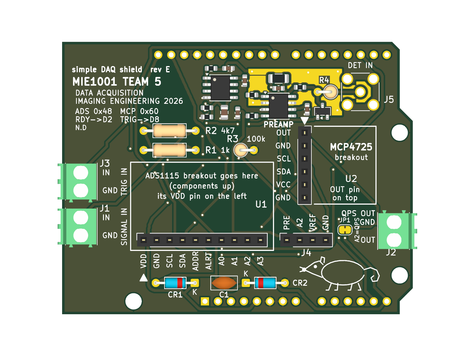
SIGNAL IN (J1) -> R2 4k7 -> [CR1/CR2 clamp, C1 filter] -> ADS1115 breakout A0 -> I2C -> UNO -> USB -> laptop
UNO -> I2C -> SparkFun MCP4725 breakout OUT -> QPS OUT (J2), 0-5 V  (JP1, bridged: also -> ADS1115 A2 read-back)
TRIG IN (J3) -> R1 1k -> UNO D8 (R3 100k to GND)    ADS1115 ALRT -> UNO D2
Faraday cup -> J5 SMA -> R4 10k -> CR3 clamp to VREF -> R5 1k -> U3 LMP7721 preamp (R6 100M || C2 10p)
            -> R11/C6 1k/1u -> ADS1115 A1 (PRE_OUT)      VREF 2.5 V (R8/R9 100k/100k + C4 -> U4A MCP6002 -> R10 -> C5) -> A3
J4 = test header: 1 PRE_OUT, 2 A2 (QPS read-back while JP1 is bridged), 3 VREF, 4 GND
I2C: UNO SDA/SCL header pins AND A4/A5 (rev E)| Check | Result |
|---|---|
| ERC | 0 errors, 0 warnings |
Guard check (check_guard.py, rev E) | PASS: 0 items of any other net within 1.0 mm of the preamp input (COAX_IN, DET_IN, TIA_IN, TIA_REF), every input item has guard copper within 0.6 mm, and the bare-board flood fill from the input reaches only VREF and TIA_OUT on F.Cu and only VREF on B.Cu. The same script FAILS on the rev D board (7 leakage paths), so it catches the rev D defect |
| Independent critical review | Two reviews against the Adafruit, SparkFun, Arduino, Phoenix and TI source files and datasheets. Rev A: pinouts and UNO geometry correct, four fixes → rev B. Rev C: copper clean, no respin needed; one wrong BOM part number and several wrong claims in this file, all corrected below |
| Host board | Arduino UNO R3 SMD (ATmega328P in a flat TQFP-32 package). Its headers are identical to the standard R3 (same positions, same pins, SDA/SCL next to AREF), so the shield fits unchanged |
| Still unverified | The height of the parts on the UNO under the shield (crystal, USB chip, capacitors). The SMD chip itself is only about 1.2 mm tall, so this is much less of a risk than with the socketed DIP chip, but look at your board before soldering |
| DRC incl. schematic parity | 0 errors, 0 unconnected, 0 parity issues (4 lib_footprint_mismatch warnings: ARD1 and J1–J3 are deliberately modified copies) — rev E |
| Orientation | Same real-UNO geometry as the full board (rev E): flipped library footprint, keep-outs over the USB, DC jack and both ICSP headers |
| Rules | 0.5 mm tracks, ≥ 0.3 mm gaps, 0.8/0.4 mm vias: far above the Digi-Key PCB Builder (5 mil / 8 mil) and JLCPCB minimums |
An independent review of rev D found a leakage path and a few smaller problems. No connector, socket or mounting hole moved (J1–J5, the two breakout sockets, H1–H3 are where they were in rev D). The router re-laid most of the signal tracks because the obstacles changed; that does not matter electrically, DRC and the guard check are clean.
check_guard.py is strict now. It fails (exit 1) on any unguarded input item (it used to only
print them) and adds a bare-board flood fill from the input nets on each copper layer: reaching
copper of any net other than VREF / TIA_OUT, or leaving the guard area, fails the build.
check_guard.py .history/revD-final/mie1001_daq_simple.kicad_pcb shows the rev D failure.ads.readADC_SingleEnded(2), with the ±6.144 V range
(ads.setGain(GAIN_TWOTHIRDS)), because 0–5 V does not fit the ±4.096 V range. To use A2 for something else, cut the thin copper
bridge between JP1's pads with a knife (check with a meter); a blob of solder closes it again.
JP1 is next to J4, marked "JP1 / A2=QPS".The Faraday cup gives a current of pA to nA. The ADS1115 measures voltage, so rev D adds a transimpedance amplifier (U3, LMP7721) that turns 1 nA into 0.1 V. Everything that was on rev C stays where it was; the preamp sits in the band under the digital header, where the text used to be (the text moved to the left edge and the back).
| Part | Job |
|---|---|
| J5 SMA jack (vertical, PTFE) | Detector input. Use a BNC-female to SMA-male adapter for a BNC cable. A BNC did not fit anywhere on this board |
| U3 LMP7721 + R6 100 MΩ | The preamp: Vout = VREF − I × 100 MΩ. Full scale ~25 nA; 1 ADC count = 1.25 pA at GAIN_ONE |
| C2 10 pF | Stops the preamp oscillating with the cable capacitance. Sets a 159 Hz bandwidth |
| R4 10k + CR3 BAV199 + R5 1k | Protect U3 from a discharge on the cable. CR3 is tied to VREF, so it leaks ~0 into the input |
| VREF 2.5 V: R8/R9 100k/100k (rev E), C4 10 µF, U4A MCP6002, R10 100 Ω, C5 1 µF | The input sits at 2.5 V so the output can swing both ways on a single 5 V supply |
| R7 1k | Protects U3's + input |
| R11 1k + C6 1 µF | 159 Hz anti-alias filter before ADS1115 A1 |
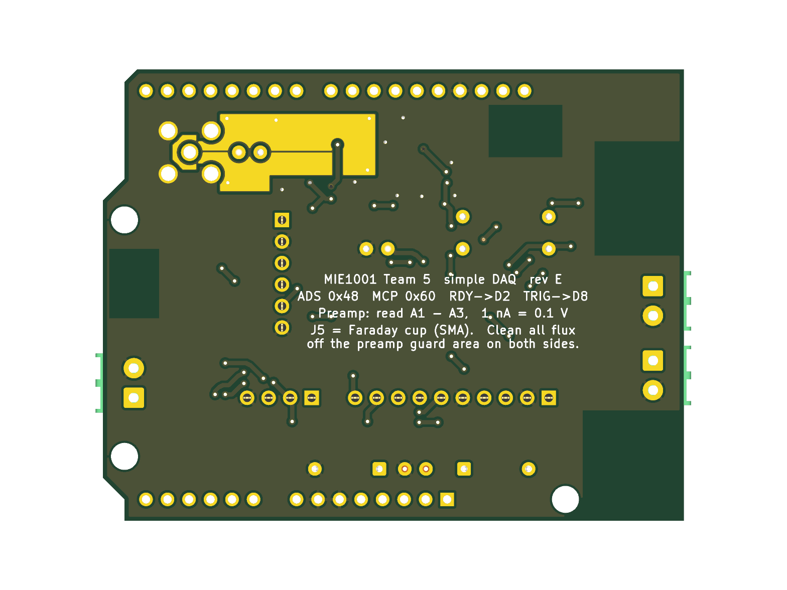
| Guard ring (copper at VREF, both layers, no solder mask) | Surrounds the whole input so no other copper can leak pA into it; closed under U3 between pins 2 and 7 (rev E) |
Firmware: read the preamp as ads.readADC_Differential_1_3() (A1 − A3 = PRE_OUT − VREF), then
I = −V / 100e6. The ADS1115 only offers the pairs 0-1, 0-3, 1-3 and 2-3, which is why VREF is on A3.
SIGNAL IN (J1) → A0 still works as before for a voltage input.
J4 changed: pin 1 is now PRE_OUT and pin 3 is VREF (monitor only: connect a meter or scope, never a source). Pin 2 (A2) carries the QPS read-back while JP1 is bridged (rev E); cut JP1 to use it as a free input.
Still 0-5 V on QPS OUT. The Extrel 150-QC wants a 0-10 V mass command; that needs a gain-2 amplifier on a supply above 10 V (e.g. a 12 V adapter on the UNO's DC jack). Not on this revision.
Handling: the input works at picoamps. After soldering, wash off all flux around U3, R6, C2, R4 and J5 (isopropyl alcohol, then dry), handle the board by its edges, and measure the zero offset with the cable connected and the beam off before every scan.
Three parts on the signal input, in the free band under the ADS1115 socket:
ads.setGain(...) instead of another chip. Note that at the highest
gains the chip's differential input resistance falls to about 710 k, where R2 costs ~0.66 % of
gain (under 0.1 % at the ±6.144 V range, 0.2–0.4 % at ±2.048 and ±1.024 V): calibrate if you use GAIN_SIXTEEN. Note TI suggests keeping
a filter resistor under 1 k; 4.7 k is deliberate here, chosen for protection, and C1 at the pin
supplies the sampling charge that the series resistance otherwise would.Watch the stripe when soldering the diodes. The silkscreen prints K at the cathode end of each one, and that is the end with the black band on the part. CR1's K points right, towards +5 V. CR2's K points left, towards the signal. Backwards, they short the signal to a rail.
dac.begin(0x60) (the library default is 0x62), and the BOM no
longer orders the new two-row ADS1115 board that doesn't fit.fab/print_1to1_top.pdf at 100 % and lay the UNO and both breakouts on it. The
header holes must line up with the UNO's pins and with each breakout's pins.BOM.csv)| Ref | Part | Where |
|---|---|---|
| U1 | Adafruit ADS1115 breakout (original, 1×10), from the class kit | plugs into a 1×10 female header (Sullins PPTC101LFBN-RC, Digi-Key S7008-ND). Don't order 1528-1085-ND: that is the new two-row board |
| U2 | SparkFun MCP4725 breakout BOB-12918 | plugs into a 1×6 female header (PPTC061LFBN-RC, S7004-ND). Retired at SparkFun, still Active at Digi-Key 1568-12918-ND (656 in stock on 2026-09-25). If it is gone, use the class-kit board: Adafruit's MCP4725 breakout is not pin-compatible (VIN/GND/SCL/SDA/A0/VOUT, no second GND) |
| J1, J2, J3 | Phoenix 1984617 screw terminals, 3.5 mm | Digi-Key 277-1721-ND |
| J4 | 1×4 female header for the spare inputs | S7002-ND |
| R1 | 1k ¼ W resistor on the trigger | 1.0KQBK-ND |
| R2 | 4k7 ¼ W resistor in series with SIGNAL IN | 13-CFR-25JB-52-4K7-ND |
| R3 | 100k ¼ W pull-down on D8, mounted standing up | 13-CFR-25JB-52-100K-ND |
| C1 | 100 nF 50 V X7R disc, 2.5 mm lead pitch (not Y5V: BC1160-ND is the wrong one) | BC1084CT-ND |
| CR1, CR2 | 1N4148 signal diodes (DO-35) | 1N4148FS-ND |
| — | UNO stacking headers (1×10, 2× 1×8, 1×6, 10.5 mm legs) | Adafruit 85, Digi-Key 1528-1074-ND (legs just clear the USB jack) |
| U3, U4, CR3, R5–R11, C2–C7, J5, R4 | the preamp | all Digi-Key, see BOM.csv / fab/digikey_bom.csv |
No other parts. Both breakouts already carry the I²C pull-ups: the ADS1115 board has 10k on SDA and on SCL (hard-wired), the MCP4725 board has 4.7k on each through jumper SJ1 (closed by a trace from the factory). In parallel that is 3.2k per line, about 2.9k once the Arduino's own internal pull-ups are counted, which draws 1.6 mA at the low level against the 3 mA an I²C device must sink. The minimum sensible value here is about 1.5k, so this is fine and the shield adds no pull-ups of its own. If you ever chain more I²C boards onto this one, each brings its own pull-ups and the total drops: cut SJ1 on the MCP4725 board to take its 4.7k pair off the bus. The ADS1115 breakout also pulls ALRT (UNO pin D2) up with 10k.
Everything is bought from Digi-Key (university procurement). Checked on digikey.com on 2026-09-25:
every part number below exists, matches the MPN and package in BOM.csv, is Active and is in stock.
fab/digikey_bom.csv./build.sh writes fab/digikey_bom.csv in Digi-Key's BOM Manager / "Upload a list" format
(Digi-Key Part Number, Manufacturer Part Number, Manufacturer, Quantity, Customer Reference), 24 lines,
quantities for ONE board. Not in it (do not order): the UNO (ARD1) and the ADS1115 breakout (U1),
both from the class kit. Upload it, then set the quantities you want (below).
| Ref | Digi-Key P/N | MPN | Stock 2026-09-25 | Unit price (USD, qty for 1 board) |
|---|---|---|---|---|
| C1 | BC1084CT-ND | Vishay K104K15X7RF5TL2 | 209,208 | 0.29 |
| C2 | 1276-1027-1-ND | Samsung CL10C100JB8NNNC | 289,398 | 0.10 |
| C3, C7 | 732-8013-1-ND | Würth 885012206095 | 508,777 | 0.10 |
| C4 | 587-4334-1-ND | Taiyo Yuden TMK212BBJ106KGHT | 13,242 | 0.29 |
| C5, C6 | 1276-1102-1-ND | Samsung CL10A105KA8NNNC | 734 | 0.10 |
| CR1, CR2 | 1N4148FS-ND | onsemi 1N4148 | 663,443 | 0.10 |
| CR3 | BAV199LT1GOSCT-ND | onsemi BAV199LT1G | 290,353 | 0.16 |
| J1–J3 | 277-1721-ND | Phoenix 1984617 | 44,569 | 0.59 |
| J4 | S7002-ND | Sullins PPTC041LFBN-RC | 46,150 | 0.42 |
| J5 | ACX1230-ND | Amphenol RF 132134 | 23,380 | 9.98 |
| R1 | 1.0KQBK-ND | YAGEO CFR-25JB-52-1K | 200,942 | 0.10 |
| R2 | 13-CFR-25JB-52-4K7-ND | YAGEO CFR-25JB-52-4K7 | 109,075 | 0.10 |
| R3 | 13-CFR-25JB-52-100K-ND | YAGEO CFR-25JB-52-100K | 92,597 | 0.11 |
| R4 | 13-CFR-25JB-52-10K-ND | YAGEO CFR-25JB-52-10K | 148,616 | 0.10 |
| R5, R7, R11 | 311-1.00KHRCT-ND | YAGEO RC0603FR-071KL | 3,768,097 | 0.10 |
| R6 | HVCB1206FKC100MCT-ND | Stackpole HVCB1206FKC100M | 19,674 | 4.01 |
| R8, R9 | 311-100KHRCT-ND | YAGEO RC0603FR-07100KL | 916,017 | 0.10 |
| R10 | 311-100HRCT-ND | YAGEO RC0603FR-07100RL | 260,261 | 0.10 |
| U2 | 1568-12918-ND | SparkFun 12918 (BOB-12918) | 656 | 6.95 |
| U3 | LMP7721MA/NOPB-ND | TI LMP7721MA/NOPB | 2,191 | 7.34 |
| U4 | MCP6002-I/SN-ND | Microchip MCP6002-I/SN | 11,665 | 0.42 |
| X1 | S7008-ND | Sullins PPTC101LFBN-RC | 24,605 | 0.64 |
| X2 | S7004-ND | Sullins PPTC061LFBN-RC | 30,030 | 0.47 |
| stacking headers | 1528-1074-ND | Adafruit 85 | 814 | 1.95 |
Changed on 2026-09-25 for Digi-Key: C2 (Murata GRM1885C1H100JA01D is Not For New Designs) → Samsung
CL10C100JB8NNNC, same 10 pF C0G 50 V 0603. C3/C7 (Samsung CL10B104KB8NNNC, 0 in stock, 61-week lead
time) → Würth 885012206095, same 100 nF X7R 50 V 0603. C4 (Samsung CL21A106KAYNNNE, 0 in stock) → Taiyo
Yuden TMK212BBJ106KGHT, same 10 µF X5R 25 V 0805 (1.35 mm max height). R4: the old number 10KQBK-ND no longer
shows up at Digi-Key; same Yageo part under 13-CFR-25JB-52-10K-ND. The LCSC column in BOM.csv is only for
the optional JLC route and may name an equivalent part (R6: Uniroyal), not the Digi-Key MPN.
Watch before ordering: C5/C6 had only 734 in stock (2 needed); if it has run out, any 1 µF ≥ 16 V X5R/X7R 0603 will do. The LMP7721 has no pin-compatible substitute: if LMP7721MA/NOPB-ND is gone, LMP7721MAX/NOPB is the same part on a reel (drop-in; check whether Digi-Key sells it as cut tape); anything else (e.g. ADA4530-1, LMC6001) has a different pinout/package and means a PCB respin.
Cost (Digi-Key qty-1 prices, USD, parts only, excl. PCB, shipping and VAT): 1 board $36.40, 2 boards $72.80 (Teams 4+5 may want a spare). The two biggest items are J5 SMA ($9.98) and U3 ($7.34).
Recommended spares (cheap, and small parts get lost or damaged in hand-soldering):
Digi-Key does not make or assemble boards itself; its PCB Builder (digikey.com/en/pcb-builder, needs a My DigiKey login to check out) uploads your files and shows live offers from partner board houses, which ship directly to you: DKRed (Digi-Key's own budget programme, built in Hollister CA), Summit Interconnect, Advanced Circuits and Precision PCBs.
Files: upload fab/mie1001_daq_simple_gerbers.zip (RS-274X Gerbers + Excellon drill, < 10 MB).
Digi-Key requires at least 2 copper layers, a drill file, 2 solder-mask layers and an outline; the zip
has all of them (F/B_Cu, F/B_Mask, F/B_Silkscreen, Edge_Cuts, PTH + NPTH drill). Digi-Key's FAQ lists
extensions such as .gts/.gto/.drl/.gko and does not name KiCad's .gtl/.gbl/.gm1: check the viewer
and assign top copper = .gtl, bottom copper = .gbl, outline = .gm1 by hand if it guesses wrong.
F_Paste and the .gbrjob are not needed (no stencil: hand-soldered).
Capabilities vs this board (checked from the .kicad_pcb, not just the rules):
| this board | DKRed | Advanced Circuits / Summit / Precision | |
|---|---|---|---|
| layers, thickness | 2, 1.6 mm FR4 | 2 or 4, 0.062" (1.6 mm) FR4 Tg170 | 2/4/6, 0.031/0.062/0.093" |
| min track / space | 0.5 mm / ≥ 0.3 mm (DRC min), zone min width 0.2 mm | 5 mil (0.13 mm) | 5, 6 or 8 mil |
| min drill | 0.4 mm (vias) | 8 mil (0.20 mm) | 8, 11 or 12 mil |
| annular ring | ≥ 0.2 mm (vias 0.8/0.4), ≥ 0.27 mm pads | ≥ 3 mil | – |
| board size | 68.58 × 53.34 mm (2.70 × 2.10 in) | 0.5–10 in | AC 0.75–10 in, Summit 2–16 × 2–22 in, Precision 1–18 in |
| finish / mask | guard copper deliberately without mask | ENIG only, red mask, white silk | HASL (leaded or lead-free) or ENIG; green/black/red/blue/purple/clear mask |
Nothing fails: every rule has ≥ 2× margin. The unmasked guard ring is just openings in the F/B_Mask Gerbers, which every house reproduces; the mask web between the bare guard and any other copper is ≥ 0.4 mm. ENIG (DKRed's only option) is the better finish here anyway: flat pads for the SOIC/0603 parts and gold on the exposed guard copper. If you pick another house, choose ENIG or lead-free HASL.
Price: DKRed is $1.50 per square inch per board, minimum 4 boards: 5.67 in² → $8.50/board, $34 for 4 (you cannot order just 3; 4 is the cheapest option). Build time 10 business days (5 quick-turn). The other houses quote live after the upload (not published; typically more). DKRed ships free only within the US: shipping to the Netherlands, customs and VAT are extra: check the total at checkout before committing.
Only if procurement allows it. Upload the same gerber zip (2 layers, 1.6 mm, HASL or ENIG). To have JLC
assemble the SMD preamp parts, turn on PCB Assembly (top side) and upload fab/jlcpcb_bom.csv and
fab/jlcpcb_cpl.csv (16 parts, 11 lines, from the LCSC column); check U3/U4/CR3 rotation in JLC's preview
and that the LCSC parts are in stock. Then solder only the THT steps below.
Nothing is assembled by the board house. Work on an ESD mat with a grounded wrist strap, fine tip (≤ 1 mm chisel), 0.5 mm solder, flux pen, fine tweezers and a magnifier. Solder all SMD parts first, while the board still lies flat, then the THT parts from lowest to tallest.
Hard to hand-solder: the 0603 parts (small, unmarked caps: C2 mixed up with another cap ruins the preamp's stability), CR3 (SOT-23), and J5 (ground legs on a big pour, next to the bare guard). U3 is easy to solder but easy to kill with ESD and easy to spoil with flux: this is why it gets a spare. None of the parts needs hot air or reflow.
dac.begin(0x60): the Adafruit_MCP4725 library defaults to 0x62, so a plain dac.begin()
finds nothing. ads.begin() (0x48) is correct as is.ads.setGain(GAIN_TWOTHIRDS) gives ±6.144 V full scale. For a small
signal turn the gain up instead of adding an amplifier: GAIN_SIXTEEN gives ±0.256 V full scale
and ~7.8 µV steps.RATE_ADS1115_250SPS, 4 ms) and average
5, 10, 50 ... consecutive readings (20, 40, 200 ms). Time the samples with the ALRT/RDY pin (D2),
not with delay(). C1 barely touches 50 Hz. Measure the result with the input shorted.pinMode(8, INPUT), active HIGH. R3 holds D8 low when nothing is connected. Use 5 V
logic if you can: the ATmega needs 3.0 V for a HIGH, so 3.3 V logic (3.27 V at D8 after the R1/R3 divider) has under 0.3 V to spare.
R1 limits the current if the trigger goes a little above 5 V. Never feed it 12 V: that pushes
6.5 mA into the ATmega's input clamp, past its absolute maximum.pinMode(2, INPUT) is enough, the breakout has the pull-up. (The diodes are named CR1 and CR2 and the UNO is ARD1, so "D2" and "A1" on this board
always mean the UNO's pins.)../mie1001_daq_board, rev E)Since rev D this board also has an electrometer preamp (U3 LMP7721, 100 MΩ, guarded input on J5), so
it can measure a Faraday-cup current directly, with a single fixed range (~25 nA full scale). SIGNAL IN
(J1) still digitises a voltage that someone else has made, with basic protection (R2, CR1/CR2) and a
339 Hz filter (R2, C1). The full board (../mie1001_daq_board) adds a jumper-selectable second
feedback range (2.2 MΩ / 100 MΩ); this one stays easy to build, with the breakouts from class plugged in.
generate_schematic.py and generate_pcb.py generate everything (the PCB script reuses the
UNO geometry and the router of the full board); ./build.sh rebuilds and re-runs all checks.
The possum and the prayer to the machine gods are in generate_pcb.py, possum().
| Qty | Value | Footprint | References |
|---|---|---|---|
| 6 | 1k | Resistor_SMD:R_0603_1608Metric | R3, R4, R9, R13, R16, R17 |
| 5 | 10k | Resistor_SMD:R_0603_1608Metric | R7, R8, R10, R11, R14 |
| 4 | 100nF | Capacitor_SMD:C_0603_1608Metric | C4, C5, C6, C8 |
| 3 | 1uF | Capacitor_SMD:C_0603_1608Metric | C2, C9, C10 |
| 2 | 100R | Resistor_SMD:R_0603_1608Metric | R12, R15 |
| 2 | 10uF | Capacitor_SMD:C_0805_2012Metric | C3, C7 |
| 2 | 4k7 | Resistor_SMD:R_0603_1608Metric | R5, R6 |
| 2 | MountingHole_3.2mm_M3 | MountingHole_3.2mm_M3 | H1, H2 |
| 1 | 100M | Resistor_SMD:R_1206_3216Metric | R2 |
| 1 | 10pF | Capacitor_SMD:C_0603_1608Metric | C1 |
| 1 | 2M2 | Resistor_SMD:R_0603_1608Metric | R1 |
| 1 | ADS1115IDGSR | Package_SO:MSOP-10_3x3mm_P0.5mm | U2 |
| 1 | Arduino UNO R3 | Module:Arduino_UNO_R3 | A1 |
| 1 | BAV199LT1G | Package_TO_SOT_SMD:SOT-23 | D1 |
| 1 | Detector in | Connector_Coaxial:BNC_Amphenol_031-6575_Horizontal | J1 |
| 1 | LMP7721MA/NOPB | Package_SO:SOIC-8_3.9x4.9mm_P1.27mm | U4 |
| 1 | MCP4725A0T-E/CH | Package_TO_SOT_SMD:SOT-23-6 | U1 |
| 1 | MCP6002-I/SN | Package_SO:SOIC-8_3.9x4.9mm_P1.27mm | U3 |
| 1 | QPS cmd out | TerminalBlock_Phoenix:TerminalBlock_Phoenix_PT-1,5-2-3.5-H_1x02_P3.50mm_Horizontal | J2 |
| 1 | Range select | Connector_PinHeader_2.54mm:PinHeader_1x03_P2.54mm_Vertical | JP1 |
| 1 | Trigger in | TerminalBlock_Phoenix:TerminalBlock_Phoenix_PT-1,5-2-3.5-H_1x02_P3.50mm_Horizontal | J4 |
| 1 | VREF/AIN3 | Connector_PinHeader_2.54mm:PinHeader_1x03_P2.54mm_Vertical | J3 |
Chaospossum/mie1001-daq
MIE1001 Team 5: DAQ firmware and Arduino shield designs (preamp, ADS1115, MCP4725)

KrasForge/Courant
A 2D finite-difference physical-modeling synthesis engine in structural VHDL: a vibrating membrane/plate/gong solved on FPGA fabric, with a nonlinear chaos term, playable polyphonically over MIDI/CV.

Ace2932/Fennec
This project is a heavily modified fork of the open-source NovaSM3 quadruped, redesigned to serve as a research platform for embodied AI.


Mobilab-AgroTIC/debitdouille
Système pour controler le fonctionnement d'un pulvérisateur

bogdan-kovalchuk/esp32-battery-charging-monitoring
An ESP32-based 12 V battery voltage monitor. The firmware measures battery voltage, while a Flask backend delivers notifications to a Signal group through signal-cli.


It measures 68.6 × 53.3 mm and has 2 copper layers, 1.6 mm thick.
40 parts, built around the ADS1115IDGSR, MCP6002-I/SN, RC0603FR-071KL and RC0603FR-0710KL. The full list of its parts is on this page, with links to each part's symbol and footprint where PCBKit's library has them.
From the Chaospossum/mie1001-daq repository on GitHub, at the commit this page was made from: the board is hardware/mie1001_daq_board/mie1001_daq_board.kicad_pcb and its schematic hardware/mie1001_daq_board/mie1001_daq_board.kicad_sch. PCBKit opens the board in the browser, with nothing to install.
Its repository states no licence, so its author keeps all rights: ask Chaospossum before reusing the design.