2 layers50 × 50 mm
 AlanFromJapan/pcb-design
My PCBs designs
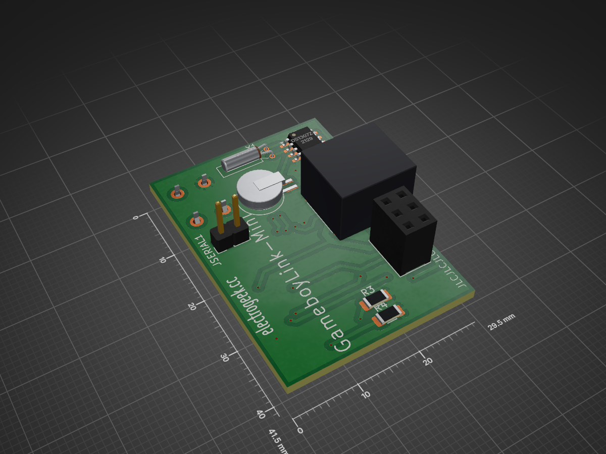
GameboyLinkMini is an open-source printed circuit board by AlanFromJapan, from the AlanFromJapan/pcb-design repository on GitHub, published under the MIT licence. It is a 2-layer board of 29.5 × 41.5 mm with 14 parts on 27 nets, routed with 158 tracks and 21 vias.
It is built around the ATTINY2313-20SU and DS1307Z+. Its parts include 4 resistors, 2 ICs, 2 diodes, 2 connectors and 1 switch. It belongs with the AVR (ATmega, ATtiny) boards of this library.


A simple NOT gate and a 555 monostable to "show" on a LED a 400 ns pulse every second that your eyes won't see otherwise.
| Qty | Value | Footprint | References |
|---|---|---|---|
| 2 | 10k | Resistor_SMD:R_1206_3216Metric_Pad1.30x1.75mm_HandSolder | R1, R2 |
| 2 | LED | LED_SMD:LED_1206_3216Metric_Pad1.42x1.75mm_HandSolder | D1, D2 |
| 2 | R | Resistor_SMD:R_1206_3216Metric_Pad1.30x1.75mm_HandSolder | R3, R4 |
| 1 | ATtiny2313-20S | Package_SO:SOIC-20W_7.5x12.8mm_P1.27mm | U1 |
| 1 | AVR-ISP-6 | Connector_PinSocket_2.54mm:PinSocket_2x03_P2.54mm_Vertical | J2 |
| 1 | Battery_Cell | Battery:BatteryHolder_Seiko_MS621F | BT1 |
| 1 | Conn_01x02 | Connector_PinHeader_2.54mm:PinHeader_1x02_P2.54mm_Vertical | JSERIAL1 |
| 1 | Crystal | Crystal:Crystal_C26-LF_D2.1mm_L6.5mm_Horizontal | Y1 |
| 1 | DS1307Z+ | Package_SO:SOIC-8_3.9x4.9mm_P1.27mm | U2 |
| 1 | SW_Reset | Button_Switch_THT:SW_PUSH_6mm | SW1 |
| 1 | ~ | kalshagar:GBA_Link_Connector_Male | J1 |


RZ3DDD/Spot_Welding_Controler
Development of a PCB for Spot_Welding_Controler

dunkelstern/NightClock
Small SMD based night clock with RTC and battery/supercap backup

DeshmukhMalhar/sch2header
Scripts to auto-generate pin defination header from schematics

pruttelherrie/Ehx9-All
Modifications for the Electro Harmonix '9' line of pedals.

reivax-boucoi/PCB_Kicad
Repo for all my home projects involving PCBs developped with Kicad


agranlund/raven
Homemade MC68060 + DSP56303 Atari-compatible computer. Hardware, firmware, and software stack
It measures 29.5 × 41.5 mm and has 2 copper layers, 1.6 mm thick.
14 parts, built around the ATTINY2313-20SU and DS1307Z+. The full list of its parts is on this page, with links to each part's symbol and footprint where PCBKit's library has them.
From the AlanFromJapan/pcb-design repository on GitHub, at the commit this page was made from: the board is GameboyLinkMini/GameboyLinkMini.kicad_pcb and its schematic BPi2m-Ethernet/BPi2m-Ethernet.kicad_sch. PCBKit opens the board in the browser, with nothing to install.
Its repository publishes it under the MIT licence: you may reuse it on that licence's terms (keep the author's notice, and for a copyleft licence share your changes alike).