2 layers60 × 52 mm
Gsm tracker
Abdullah-Atif/gsm-gps-tracker
Live vehicle tracker: ESP32 / ESP32-C3 + NEO-M8N GPS + SIM800L (2G) -> MQTT -> live web map. Firmware, KiCad PCBs, wiring diagram.
15 partsMIT

 Abdullah-Atif/gsm-gps-tracker
Live vehicle tracker: ESP32 / ESP32-C3 + NEO-M8N GPS + SIM800L (2G) -> MQTT -> live web map. Firmware, KiCad PCBs, wiring diagram.
Gsm tracker c3 is an open-source printed circuit board by Abdullah-Atif, from the Abdullah-Atif/gsm-gps-tracker repository on GitHub, published under the MIT licence. It is a 2-layer board of 53 × 52 mm with 16 parts on 10 nets, routed with 63 tracks and 19 vias.
It is built around the 100UF 10V. Its parts include 7 connectors, 3 capacitors, 2 resistors, 1 IC and 1 switch. It belongs with the radio and wireless boards of this library.
A compact 2-layer carrier PCB (60 x 52 mm) for the working tracker. The ESP32 DevKit, SIM800L module and NEO-M8N GPS plug into headers, so there is no loose wiring and no SMD soldering.
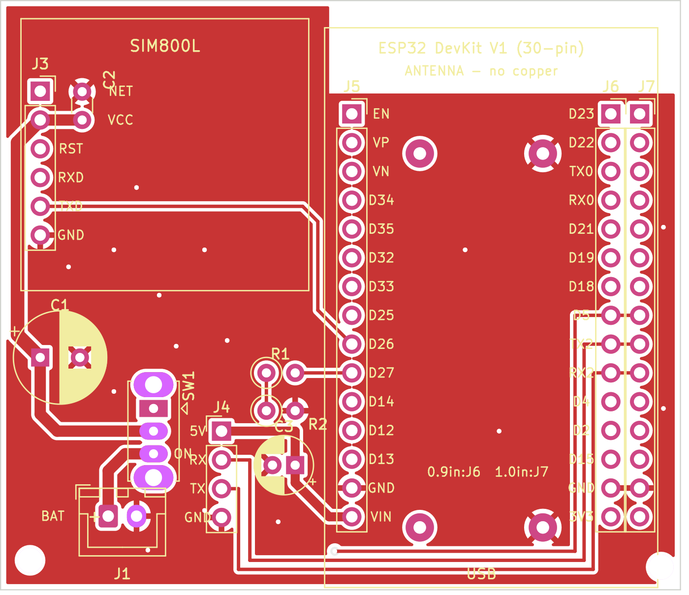
| File | Purpose |
|---|---|
gsm_tracker.kicad_pcb / .kicad_pro | KiCad 7 board (open in KiCad, or import into Altium) |
gsm_tracker_gerbers.zip | Gerber + drill files, ready to upload to JLCPCB / PCBWay |
BOM.csv | Parts list |
generate_pcb.py | Script that generates the board (re-run after changing positions) |
drc_report.txt | KiCad design-rule check report |
renders/front.png, renders/back.png | Copper + silkscreen views (back view is mirrored) |
gsm_tracker.kicad_pcb.Li-ion 1S (J1) --SW1--> VBAT --+--> SIM800L VCC (C1 1000 uF + C2 100 nF at the module)
+--> MT3608 IN+ --> 5.0 V --+--> ESP32 VIN (C3 100 uF)
+--> GPS 5V (J4)| Signal | ESP32 pin | Module pin | Notes |
|---|---|---|---|
| SIM_TXD | D26 (GPIO26) | SIM800L TXD | direct |
| SIM_RXD | D27 (GPIO27) | SIM800L RXD | 10k / 20k divider (R1, R2) |
| SIM_RST | D5 (GPIO5) | SIM800L RST | direct |
| GPS_TX | RX2 (GPIO16) | GPS TX | |
| GPS_RX | TX2 (GPIO17) | GPS RX |
These are the same pins the firmware already uses, so no firmware change is needed.
ESP32 row spacing. Measure the distance between the two pin rows of your DevKit.
Both footprints are on the board. The J6/J7 courtyard overlap in the DRC report is intentional.
SIM800L pin order. The module must sit so that its pins match the silkscreen labels: NET, VCC, RST, RXD, TXD, GND, from top to bottom.
MT3608 boost module. This needs extra care:
Battery. Use a protected 18650 cell and charge it outside the board (for example with a TP4056 module that has protection).
GPS. Connect it through J4 with a short cable and place the GPS antenna facing the sky. Keep it away from the SIM800L antenna.
| Qty | Value | Footprint | References |
|---|---|---|---|
| 2 | M2 | MountingHole_2.2mm_M2 | H1, H2 |
| 1 | 1000uF_10V | CP_Radial_D8.0mm_P3.50mm | C1 |
| 1 | 100nF | C_Disc_D3.0mm_W1.6mm_P2.50mm | C2 |
| 1 | 100uF_10V | CP_Radial_D5.0mm_P2.00mm | C3 |
| 1 | 10k | R_Axial_DIN0204_L3.6mm_D1.6mm_P5.08mm_Horizontal | R1 |
| 1 | 20k | R_Axial_DIN0204_L3.6mm_D1.6mm_P5.08mm_Horizontal | R2 |
| 1 | BATT_1S | JST_XH_B2B-XH-A_1x02_P2.50mm_Vertical | J1 |
| 1 | C3_GPIO5_21_ROW | PinSocket_1x08_P2.54mm_Vertical | J6 |
| 1 | C3_POWER_ROW | PinSocket_1x08_P2.54mm_Vertical | J5 |
| 1 | GPS | PinSocket_1x04_P2.54mm_Vertical | J4 |
| 1 | MT3608_5V | U3 | |
| 1 | PWR | SW_Slide_SPDT_Straight_CK_OS102011MS2Q | SW1 |
| 1 | SIM800L_AUDIO_17.78 | PinSocket_1x06_P2.54mm_Vertical | J8 |
| 1 | SIM800L_AUDIO_20.32 | PinSocket_1x06_P2.54mm_Vertical | J9 |
| 1 | SIM800L_IF | PinSocket_1x06_P2.54mm_Vertical | J3 |
Abdullah-Atif/gsm-gps-tracker
Live vehicle tracker: ESP32 / ESP32-C3 + NEO-M8N GPS + SIM800L (2G) -> MQTT -> live web map. Firmware, KiCad PCBs, wiring diagram.

Sid93/levram-biometric-attendance-scanner
ESP32-S3 face-recognition factory attendance terminal — firmware, KiCad PCB, OpenSCAD enclosure, BOM

xxdamlaxx/DroidVR
A DIY VR controller ecosystem — open-source hardware and firmware for SteamVR-compatible motion controllers.

8aChristian/InduLink-485
The board follows rigorous IPC (IPC-2152, IPC-2221, IPC-7351) standards, complete with galvanic isolation, industrial transient protection (TVS, Schottky, PTC Polyfuse), a wide-input step-down switching power…

pavan-firmware/EH-Master-Repo
This directory contains the KiCad Schematic and PCB Design Project for the EH Smart Switch (3X / 4X Channel with BL0942 Metering).

purpletue/TinyLilFella
An absolutely microscopic (metaphorically) microcontroller board based on an STM32C071. The name is fully deserved.

salvogendut/reverseMX4
An extension board for the Amstrad CPC which uses edge connectors instead of IDC ones


It measures 53 × 52 mm and has 2 copper layers, 1.6 mm thick.
16 parts, built around the 100UF 10V. The full list of its parts is on this page, with links to each part's symbol and footprint where PCBKit's library has them.
From the Abdullah-Atif/gsm-gps-tracker repository on GitHub, at the commit this page was made from: the board is esp32c3_supermini/pcb/gsm_tracker_c3.kicad_pcb. PCBKit opens the board in the browser, with nothing to install.
Its repository publishes it under the MIT licence: you may reuse it on that licence's terms (keep the author's notice, and for a copyleft licence share your changes alike).