
2 layers20 × 34.7 mm
Spi dediprog interface
9elements/spi_isolator_implant_pcb
Isolation board to connect programmers on an on-circuit SPI chip
8 parts2

 9elements/spi_isolator_implant_pcb2
Isolation board to connect programmers on an on-circuit SPI chip
SPI Implant is an open-source printed circuit board by 9elements, from the 9elements/spi_isolator_implant_pcb repository on GitHub. It is a 2-layer board of 25.9 × 18.9 mm with 14 parts on 25 nets, routed with 177 tracks and 22 vias.
It is built around the BAT60A. Its parts include 5 resistors, 3 connectors, 2 capacitors, 2 ICs and 1 diode.
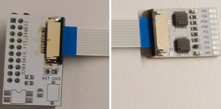 The picture shows the spi_implant on the right and the dediprog_interface on the left. The dediprog_interface is connected to the flasher (for example a dediprog). The spi_implant is supposed to be connected to the actual flash chip. The flat cable is connecting both boards. It was originally made to flash laptops and this is why it is composed of two boards (the flat cable can be more easily routed out of the laptop case).
| Qty | Value | Footprint | References |
|---|---|---|---|
| 5 | 100 | Resistor_SMD:R_0805_2012Metric | R1, R2, R3, R4, R5 |
| 2 | 100n | Capacitor_SMD:C_0805_2012Metric | C1, C2 |
| 2 | TMUX1511PWR | TMUX1511PWR:SOP65P640X120-14N | U1, U2 |
| 1 | BAT60A | Diode_SMD:D_SOD-323 | D1 |
| 1 | Conn_01x01 | Connector_Wire:SolderWirePad_1x01_SMD_1x2mm | J3 |
| 1 | Conn_01x10_Socket | Connector_FFC-FPC:TE_1-84952-0_1x10-1MP_P1.0mm_Horizontal | J1 |
| 1 | LOGO | pi_hat_spi_v2:9elogo | G*** |
| 1 | SPI_Socket | pad:wire_pad_row_1x09-2x3mm | J2 |
9elements/spi_isolator_implant_pcb
Isolation board to connect programmers on an on-circuit SPI chip
M17-Project/Module_17
M17 modem board for 9600-baud capable radios


crgarcia12/electronics-homeassistant-lightscontroll
A smart lighting controller PCB that integrates seamlessly with ESPHome and Home Assistant while maintaining full compatibility with traditional mechanical switches.


OnionDAO-git/oniondao-badge
An open-source, hacker-conference-style electronic badge built around the ESP32-S3-WROOM-1-N8R8 (8 MB flash + 8 MB Octal PSRAM), with swappable RF / audio / storage modules, an e-paper (or TFT) display socket, a secure…

It measures 25.9 × 18.9 mm and has 2 copper layers, 1.6 mm thick.
14 parts, built around the BAT60A. The full list of its parts is on this page, with links to each part's symbol and footprint where PCBKit's library has them.
From the 9elements/spi_isolator_implant_pcb repository on GitHub, at the commit this page was made from: the board is v1/spi_implant/SPI_Implant.kicad_pcb and its schematic v1/dediprog_interface/spi_dediprog_interface.kicad_sch. PCBKit opens the board in the browser, with nothing to install.
Its repository states no licence, so its author keeps all rights: ask 9elements before reusing the design.