4 layers85 × 170 mm

 8423/cryocooler-board
A 4-layer power and control board for a Ricor K508N cryocooler. It does two jobs, both controlled over I²C:
Cryocooler board is an open-source printed circuit board by 8423, from the 8423/cryocooler-board repository on GitHub. It is a 4-layer board of 58 × 49 mm with 54 parts on 27 nets, routed with 240 tracks and 165 vias.
It is built around the TPS55288RPMR, AD5258BRMZ1 and IPZ40N04S5L4R8ATMA1. Its parts include 16 capacitors, 9 resistors, 4 connectors, 3 ICs and 2 transistors. It belongs with the RP2040 boards of this library.


A 4-layer power and control board for a Ricor K508N cryocooler. It does two jobs, both controlled over I²C:
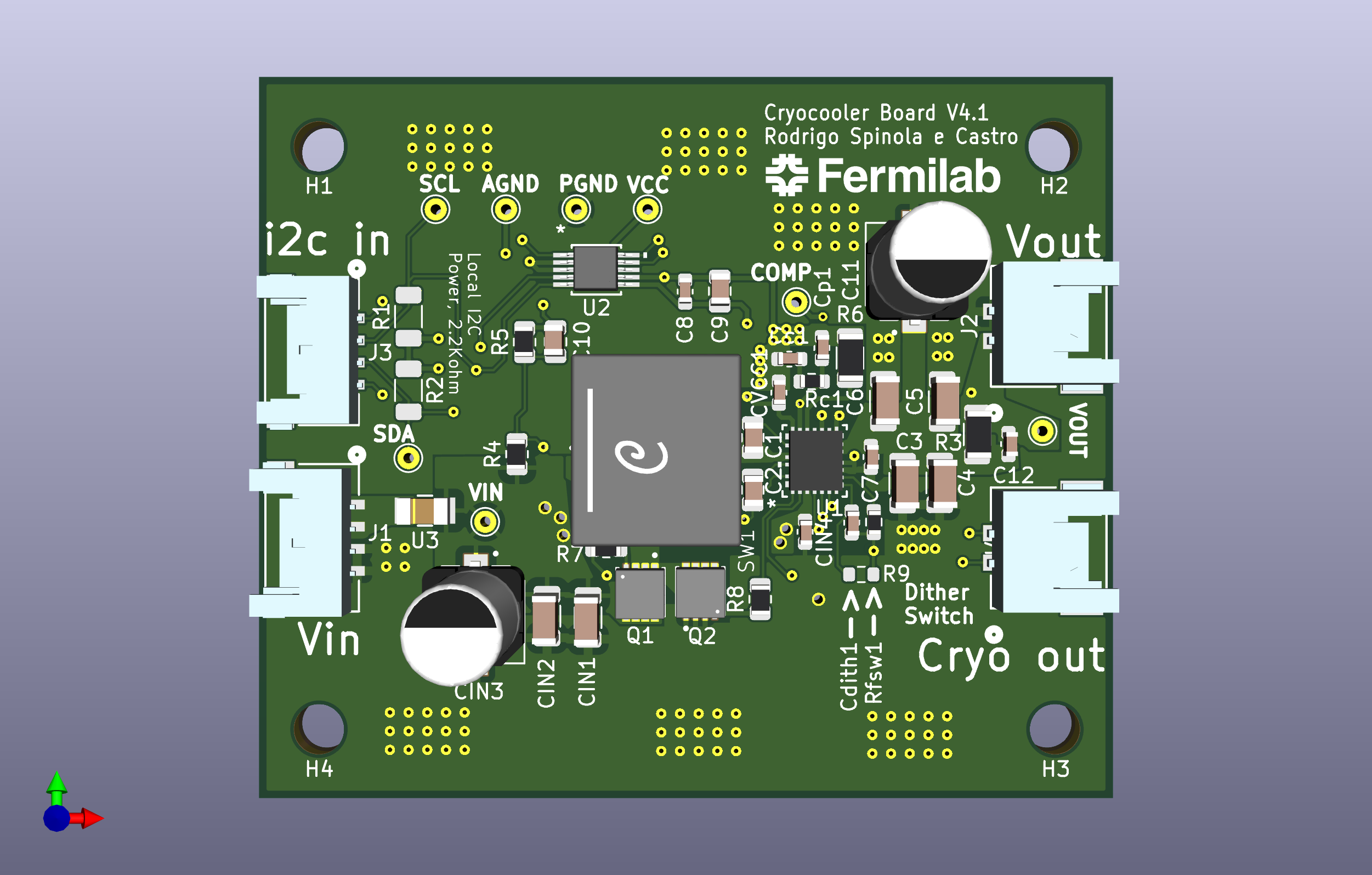
Designed in KiCad 8 by Rodrigo Spinola e Castro.
| Version | Tag | State |
|---|---|---|
| V1 | v1 | First fabricated board |
| V2 | v2 | Fabricated, faulty |
| V3 | v3 | Fabricated. I²C and digipot work; the converter output oscillates and efficiency is very low (see Lessons from V3) |
| V4 | – | Redesign addressing V3's problems: bulk output capacitor, current limit, thermal vias. Not built |
| V4.1 | v4.1 | Ordered from JLCPCB on 13 Oct 2026. A test build to confirm the control loop is stable before space-rated parts are chosen. See Changes in V4.1 |
Each built version is tagged. Browse any of them with the branch/tag selector on GitHub, or compare two, e.g. …/compare/v3...main.
| # | Requirement |
|---|---|
| 1 | Step the 24 V rail down to a set value between 12 V and 20 V. Expected load: up to ~2 A while cooling down, ~0.5 A at the set point. The cryocooler's maximum input power is 20 W. |
| 1a | The output must never exceed 24 V. |
| 1b | After a reset of I²C or of the 24 V supply, the output returns to 12 V. |
| 1c | Switching noise must not interfere with the CCD electronics, so the switching frequency stays above 500 kHz. |
| 2 | Set the cryocooler's target temperature (around 170 K) through a variable resistor. |
| 3 | Control both the output voltage and the temperature set point over I²C. |
| 4 | After a reset of I²C or of power, the temperature set point returns to 170 K. |
flowchart LR
    J1["J1<br/>24 V in"] --> U3["U3<br/>4 A fuse"] --> U1["U1 TPS55288<br/>buck-boost<br/>Q1, Q2, L1 10 µH"] --> R3["R3<br/>10 mΩ sense"] --> J2["J2<br/>12–20 V out"]
    J3["J3<br/>I²C in"] -- "0x74" --> U1
    J3 -- "0x18" --> U2["U2 AD5258<br/>1 kΩ rheostat"] --> J4["J4<br/>cryocooler<br/>set point"]
U1 -. "VCC (5 V LDO)" .-> U2All connectors are Molex Pico-Lock.
| Ref | Function | Part | Pin 1 | Pin 2 | Pin 3 | Pin 4 |
|---|---|---|---|---|---|---|
| J1 | 24 V input | 4-pin 5040500491 | VIN | VIN | PGND | PGND |
| J2 | Converter output to the cryocooler | 2-pin 2053380002 | VOUT | PGND | – | – |
| J3 | I²C | 4-pin 5040500491 | AGND | SCL | SDA | AGND |
| J4 | Cryocooler temperature set point | 2-pin 2053380002 | CRYO_2 | CRYO_1 | – | – |
On J1, each signal uses two pins in parallel.
Test points: TP_VIN1, TP_VOUT1, TP_PGND1, TP_AGND1, TP_SCL1, TP_SDA1, plus TP_COMP1 (error-amplifier output) and TP_VCC1 (gate-drive supply), new in V4.1. SW1 can be probed at the uncovered via at (129.5, 87.9) mm, on the SW1 copper beside L1; see Bring-up notes.
J1 and J3 are the same 4-pin part, and J2 and J4 are the same 2-pin part. A swapped harness puts 24 V on the I²C lines, or the converter output across the digipot. Label harnesses and check every plug before applying power.
Why this chip:
Drawbacks:
| Function | Parts | Value | Reasoning |
|---|---|---|---|
| Switching frequency | Rfsw1 | 32.4 kΩ → ≈610 kHz (datasheet Eq. 3) | Above the 500 kHz CCD limit even at the low end of tolerance with dithering (≈510 kHz), but as close as practical to the chip's typical 400 kHz |
| Inductor | L1 | 10 µH, Coilcraft XAL1010-103MED (JLC C6358489) | Gives ≈1 A ripple at the worst case (12 V out from 24 V in). The chip supports 1–10 µH; TI's evaluation board uses 4.7 µH with 3.2 A ripple at 400 kHz |
| Input-voltage turn-on | R4 / R5, C10 = 100 nF | 30 kΩ / 5.1 kΩ | Turns the converter on at ≈8 V; 24 V gives ≈3.4 V on the EN pin (limit 20 V). C10 filters the EN pin |
| Frequency dithering | Cdith1, R9 | 15 nF → ≈735 Hz modulation | Spreads switching noise over ±7 % of the frequency. R9 is an unpopulated 0 Ω across Cdith1: fit it to turn dithering off for an A/B test |
| Input fuse | U3 | 4 A, 72 V, 1206: prosemi 1206TD-4A (JLC C2838918) on the Bel C1T (0685T4000-01) footprint | Protects the 24 V bus. More than twice the expected 1–2 A, and well above the cryocooler's 20 W. Can be swapped for a jumper |
| Input capacitors | CIN1, CIN2, CIN4, CIN3 | 2 × 10 µF + 1 µF ceramic, plus 68 µF bulk | Datasheet recommends ~21 µF ceramic, plus bulk if the supply is far away; layout copied from TI's evaluation board |
| Output capacitors | C3–C6, C7, C11 | 4 × 10 µF (Samsung CL31A106KBHNNNE, 50 V X5R) + 1 µF ceramic, plus 68 µF hybrid (Panasonic EEH-ZA1V680XP) | ≈80 µF effective at 12 V and ≈74 µF at 20 V, because the ceramics lose most of their capacitance under DC bias. The compensation is designed for this. C11 is new in V4 |
| Boot capacitors | C1, C2 | 0.1 µF | As on TI's evaluation board |
| Input-side MOSFETs | Q1, Q2 | Infineon IPZ40N04S5L4R8ATMA1, with 1 Ω gate resistors R7 and R8 | As on TI's evaluation board. The 40 A rating is far more than needed. In V4.1, R7 sits next to Q1's gate, as TI's layout guide asks |
| Loop compensation | Rc1, Cc1, Cp1 | 26.1 kΩ, 5.6 nF C0G, 100 pF C0G | From the datasheet's Eqs. 24–26 with C11 fitted (C11 ESR ≈35 mΩ gives Cp ≈93 pF). TI's calculator gives crossover ≈11 kHz, 72° phase margin, 13.8 dB gain margin at 12 V out, and ≈13 kHz, 66°, 9.7 dB at 20 V out (plot below); calculated, not yet measured |
| Output current limit | R3, C12 | 10 mΩ, 1 W; 0.1 µF across it | Register 02h set to 30 mV gives a 3 A limit. C12 filters the sense lines, like C13 on TI's evaluation board. The sense point at ISP includes some output copper, so the limit may trip nearer 2.7 A |
| Average inductor current limit | R6 | 41.2 kΩ → 8 A (≈5.8 A at the low tolerance) | Well above the ≈2.75 A peak inductor current, below the inductor's saturation and the chip's switch limits. Keeps an unstable loop from damaging the board |
| I²C address | MODE pin to AGND | 0x74 | Operating mode and VCC source can then be changed over I²C |
| VCC | CVCC1, C8, C9 | 4.7 µF + 1 µF + 0.1 µF | As on TI's evaluation board (CVCC1 is the same part as its C14). CVCC1 returns to AGND, per the datasheet pin table |
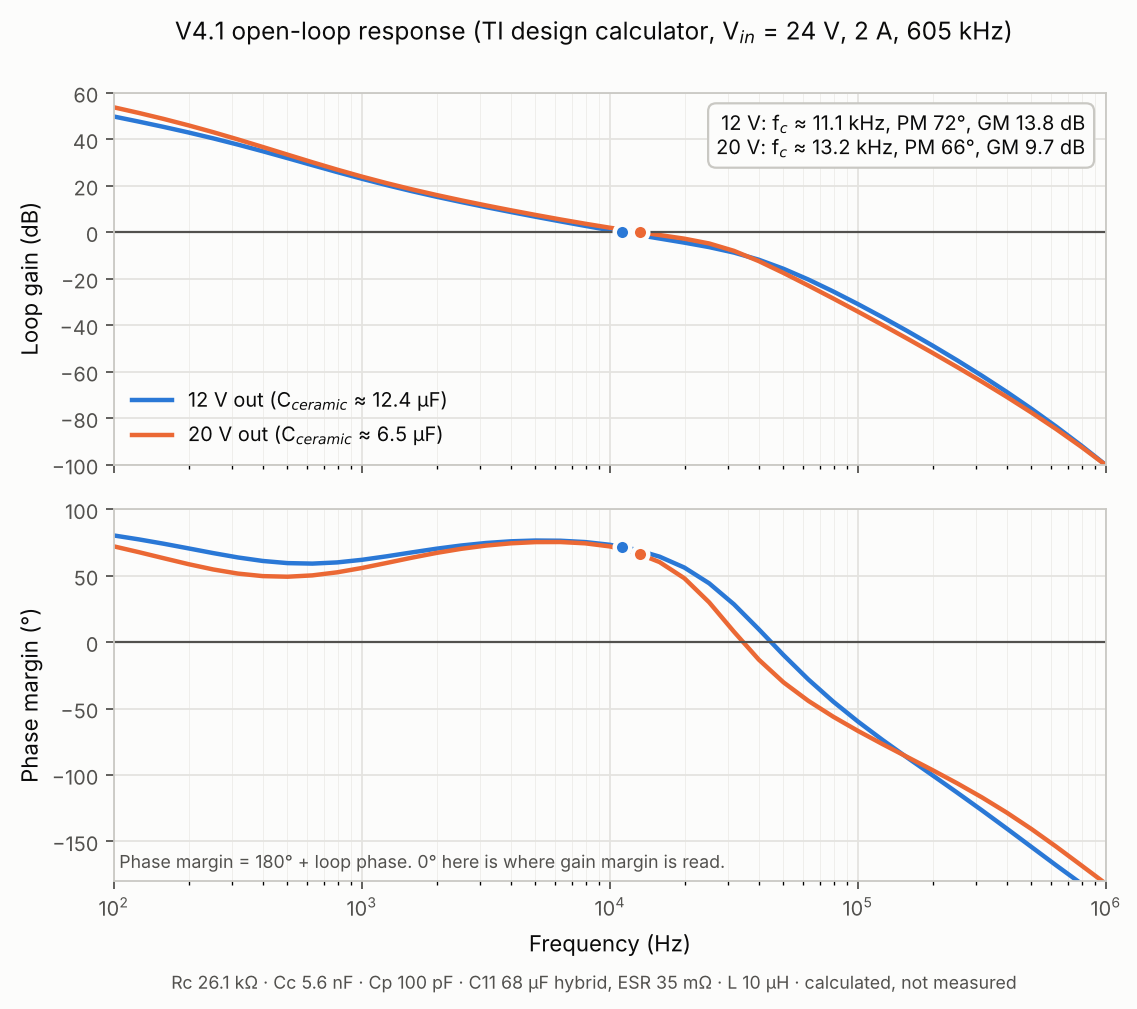
Open-loop response from TI's TPS55288 design calculator with the V4.1 values, at 24 V in, 2 A, 605 kHz. Effective ceramic output capacitance is taken from the V3 DC-bias measurement (≈12.4 µF at 12 V, ≈6.5 µF at 20 V). At 20 V the gain margin (9.7 dB) is just under TI's 10 dB guidance.
On V3, I²C and the digipot worked; the digipot covers its full 1 kΩ range. The converter did not:
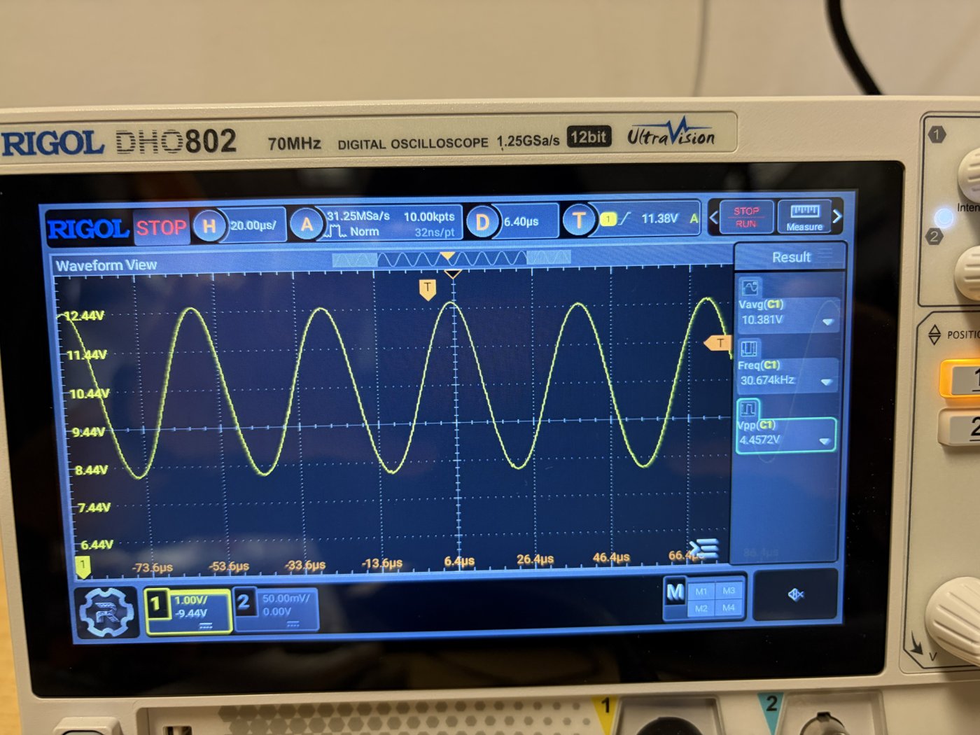
Cause: the compensation is designed for about 100 µF of output capacitance, ceramic plus electrolytic. V3 had only about 41 µF, all ceramic, and ceramic capacitors lose much of their capacitance at higher voltages. Measuring how the output decayed after setting 12 V showed ≈20 µF at 8–12 V and the full 41 µF only below 8 V. With so much less capacitance than planned, the control loop was unstable.
Changes in V4:
V4.1 is built to answer one question: is the loop stable with the bulk capacitor fitted? Changes that only matter in space (space-rated capacitors, vacuum heat path) wait until it is.
Values and parts
Additions
Layout
Schematic housekeeping
MF, MP and LCSC Part # fields. The MP is the part the LCSC number actually places, which for several V3 parts differs from the old footprint names.4 layers, 1.6 mm thick, 58 × 49 mm, with four M3 mounting holes. The stackup follows TI's evaluation board.
| Layer | Use |
|---|---|
| Top (F.Cu) | Components; copper pour mostly PGND, plus VOUT |
| In1 | PGND plane |
| In2 | Power: VCC, AGND, VIN |
| Bottom (B.Cu) | PGND plane |
| Top | In1: PGND |
|---|---|
 | 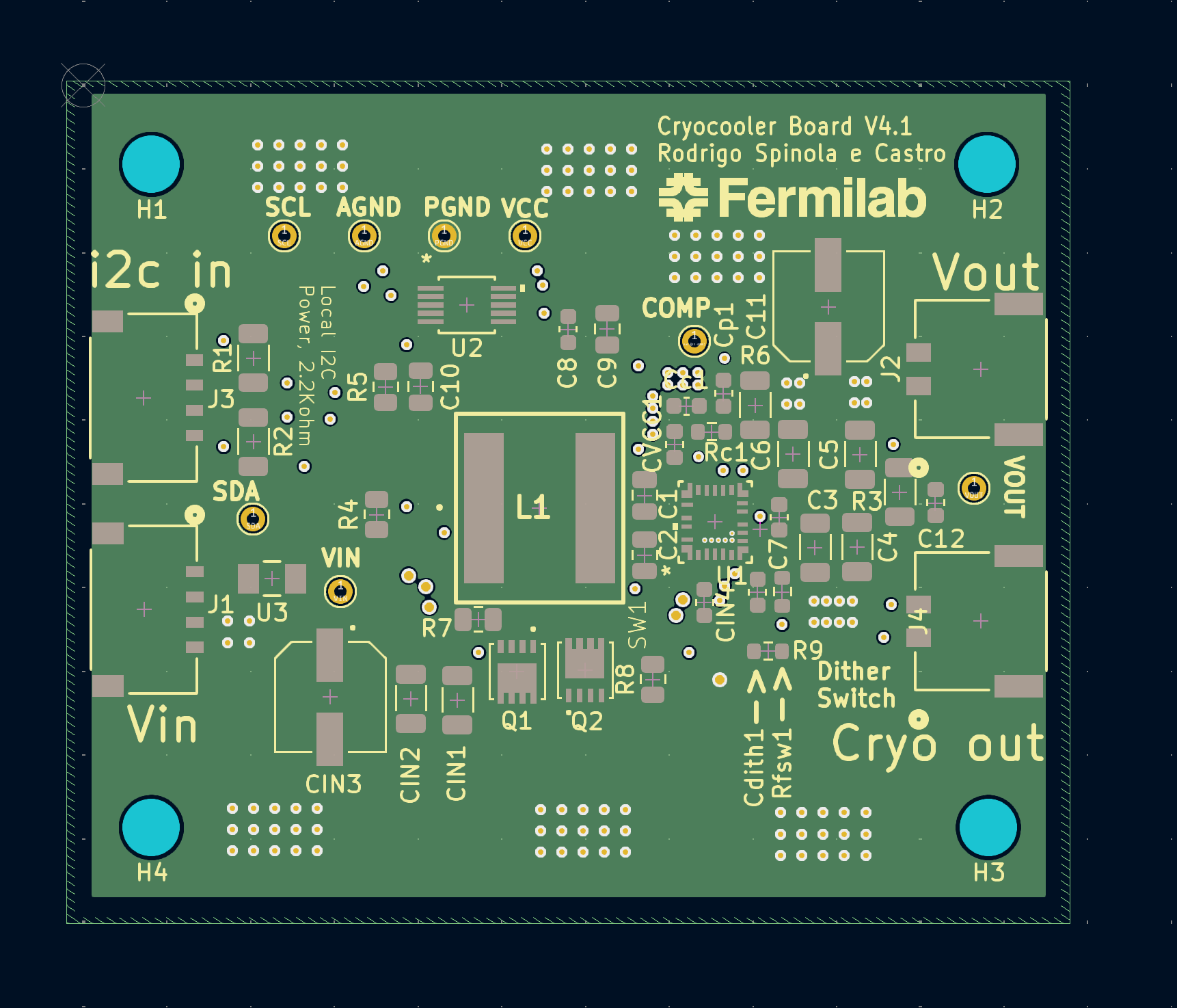 |
| In2: power | Bottom: PGND |
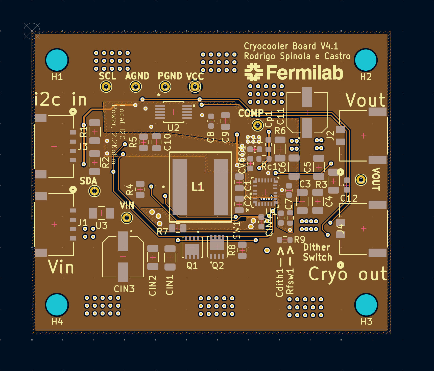 | 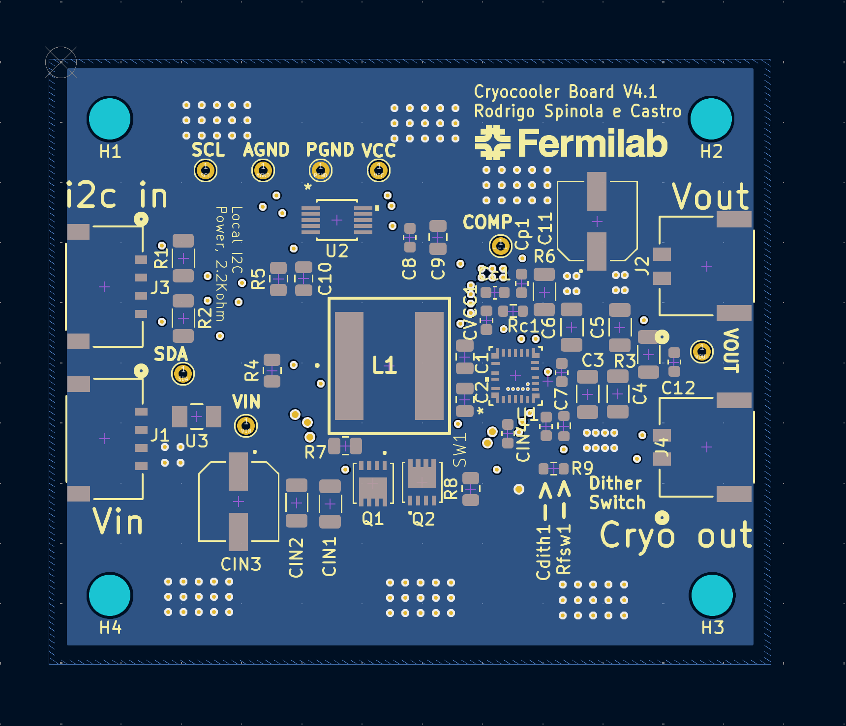 |
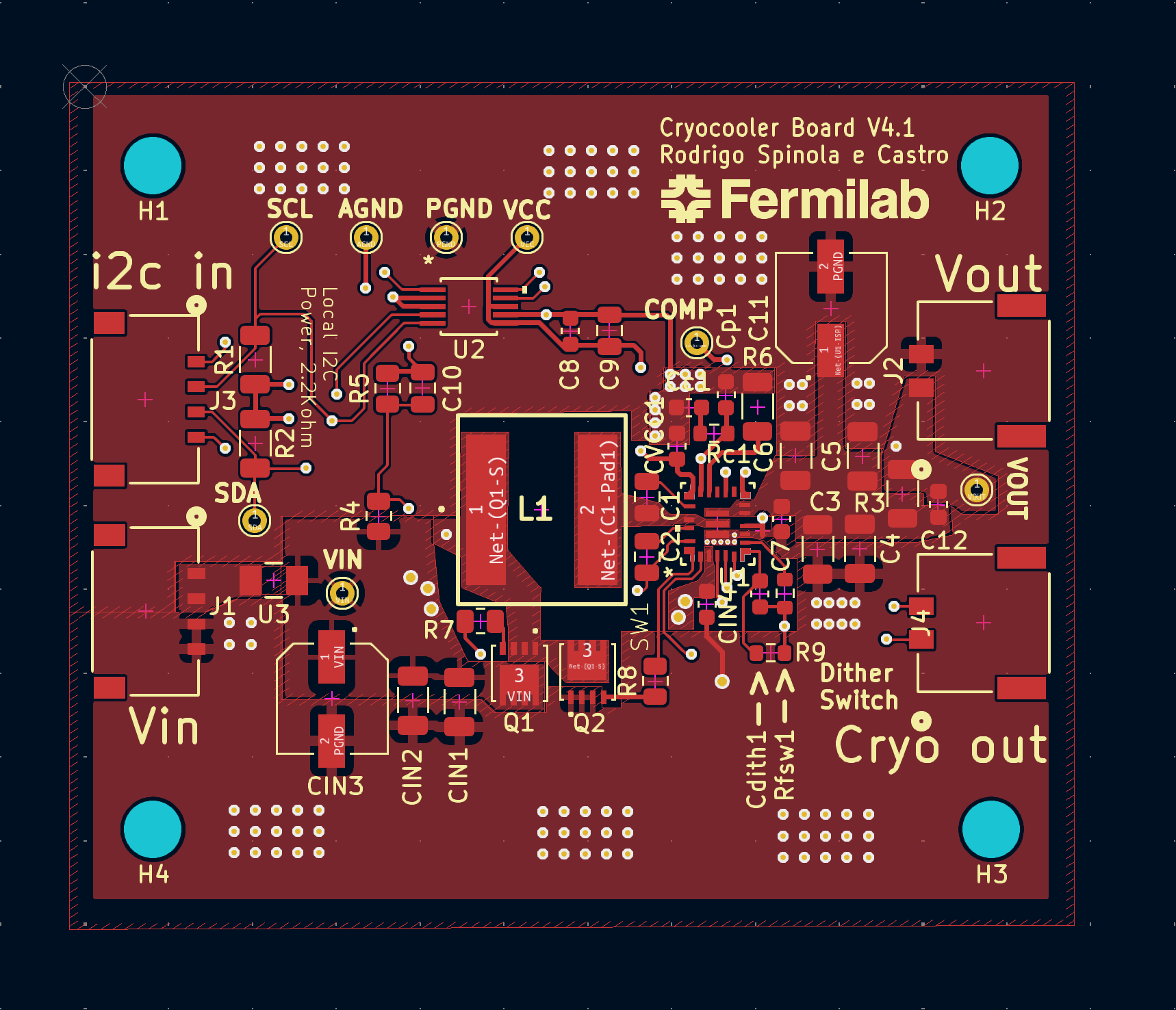
These images show V4.1 as ordered: each copper layer with the front silkscreen on top.
cryocooler-board/
├── cryocooler-board.kicad_pro / .kicad_sch / .kicad_pcb   KiCad 8 project
├── sym-lib-table, fp-lib-table                            point at lib/ (project-relative)
├── lib/
│   ├── Cryocooler.kicad_sym     custom symbols
│   ├── Cryocooler.pretty/       custom footprints
│   └── Cryocooler.3dshapes/     3D models (STEP)
├── production/                  JLCPCB files: Gerbers zip, BOM, pick-and-place
├── docs/                        switching-converter design primer, README images
└── scripts/sw1_duty_analysis.py analyse SW1 duty cycle and efficiency from scope CSVs
Opening it: clone or download, then open cryocooler-board.kicad_pro in KiCad 8. Every non-standard symbol, footprint and 3D model is in lib/, so there's nothing to install. The tags v1–v3 hold the old versions, but those used symbol libraries stored outside the project, so they may open with library warnings.
Scope analysis script:
python3 scripts/sw1_duty_analysis.py scope.csv --rload 176 --vin 24Boards are made and assembled by JLCPCB. The production files are generated with the KiCad Fabrication Toolkit into production/.
LCSC Part # field in the schematic, so the BOM names the exact JLC part. Also fill MF and MP with the part that LCSC number places.Resistor_SMD:R_0603_1608Metric and so on). Only parts with their own package have custom footprints in lib/.fabrication-toolkit-options.json: exclude DNP parts, refill zones, apply JLC rotation corrections.JLCPCB Rotation Offset field to those symbols.Carried to the test board and the flight design:
JLCPCB Rotation Offset to U2, Q1 and Q2.lib/Cryocooler.pretty/, and update the silkscreen note "Local I2C Power, 2.2 Kohm" (R1/R2 are not populated).| Qty | Value | Footprint | References |
|---|---|---|---|
| 8 | TestPoint | TestPoint:TestPoint_THTPad_D1.5mm_Drill0.7mm | TP_AGND1, TP_COMP1, TP_PGND1, TP_SCL1, TP_SDA1, TP_VCC1, TP_VIN1, TP_VOUT1 |
| 6 | 10uF | Capacitor_SMD:C_1206_3216Metric | C3, C4, C5, C6, CIN1, CIN2 |
| 4 | 0.1uF | Capacitor_SMD:C_0805_2012Metric | C1, C2, C9, C10 |
| 4 | MountingHole | Cryocooler:M3_3_4mm_hole | H1, H2, H3, H4 |
| 3 | 1uF | Capacitor_SMD:C_0603_1608Metric | C7, C8, CIN4 |
| 2 | 1 ohm | Resistor_SMD:R_0805_2012Metric | R7, R8 |
| 2 | 2.20k | Resistor_SMD:R_1206_3216Metric | R1, R2 |
| 2 | 68uF | Cryocooler:EEH-ZA1V680XP | C11, CIN3 |
| 2 | IPZ40N04S5L4R8ATMA1 | Cryocooler:IPZ40N04S5L4R8ATMA1 | Q1, Q2 |
| 2 | MOL Pico 2 | Cryocooler:MOLEX_2_pin | J2, J4 |
| 2 | MOL Pico 4 | Cryocooler:MOLEX_4_pin | J1, J3 |
| 1 | 0 Ohm | Resistor_SMD:R_0603_1608Metric | R9 |
| 1 | 0.1uF | Capacitor_SMD:C_0603_1608Metric | C12 |
| 1 | 100pF | Capacitor_SMD:C_0603_1608Metric | Cp1 |
| 1 | 10mOhm | Resistor_SMD:R_1206_3216Metric | R3 |
| 1 | 10uH | Cryocooler:XAL1010 | L1 |
| 1 | 15nF | Capacitor_SMD:C_0603_1608Metric | Cdith1 |
| 1 | 26.1k | Resistor_SMD:R_0603_1608Metric | Rc1 |
| 1 | 30k | Resistor_SMD:R_0805_2012Metric | R4 |
| 1 | 32.4K | Resistor_SMD:R_0603_1608Metric | Rfsw1 |
| 1 | 4.7uF | Capacitor_SMD:C_0603_1608Metric | CVCC1 |
| 1 | 41.2K | Resistor_SMD:R_1206_3216Metric | R6 |
| 1 | 4A Fuse | Cryocooler:0685T4000-01 | U3 |
| 1 | 5.1k | Resistor_SMD:R_0805_2012Metric | R5 |
| 1 | 5.6nF | Capacitor_SMD:C_0603_1608Metric | Cc1 |
| 1 | AD5258BRMZ1 | Cryocooler:AD5258BRMZ1_IC | U2 |
| 1 | NetTie_2 | Cryocooler:NetTie-2_SMD_Pad0.3mm | NT1 |
| 1 | TPS55288RPMR | Cryocooler:TPS55288 | U1 |
It measures 58 × 49 mm and has 4 copper layers, 1.6 mm thick.
54 parts, built around the TPS55288RPMR, AD5258BRMZ1 and IPZ40N04S5L4R8ATMA1. The full list of its parts is on this page, with links to each part's symbol and footprint where PCBKit's library has them.
From the 8423/cryocooler-board repository on GitHub, at the commit this page was made from: the board is cryocooler-board.kicad_pcb and its schematic cryocooler-board.kicad_sch. PCBKit opens the board in the browser, with nothing to install.
Its repository states no licence, so its author keeps all rights: ask 8423 before reusing the design.


hydazz/iasis
An optional Raspberry Pi Compute Module 5 carrier for Iasis. It plugs into the main board's HubPD population and carries Ethernet, NVMe storage, an accessory USB-C port and a service USB-C port.

mikesmitty/power-manifold
Six-port USB-C power supply: up to 100 W per port from one 24 V supply, with per-port control, priority-based power sharing and Home Assistant support. 100% local, no cloud required.

gschuurman/android_vendor_gschuurman_vehicle_interfaces
vehicle interfaces for android automotive for a custom headunit


gusmanb/logicanalyzer
24 channel, 100Msps logic analyzer hardware and software