
4 layers288 × 135.4 mm
Keyboard v2
ben5049/Keyboard
Features: - Wireless - 900mAh battery - Bluetooth (nRF52) - ZMK - 4 Port USB hub - BLDC Knob for haptic feedback - Kailh Choc V1 switches
344 parts1Apache-2.0

uConsole External I/O Breakout
Ext pcb is an open-source printed circuit board by 57Bravo, from the 57Bravo/uConsole_Ext_IO_Breakout repository on GitHub. It is a 2-layer board of 78 × 37.5 mm with 25 parts on 39 nets, routed with 634 tracks and 63 vias.
It is built around the SM04B-SRSS-TB(LF)(SN), GSB12J21C1EU and S2B-XH-A(LF)(SN), with the SFW15R-2STE1LF among its other parts. It belongs with the interfaces and adapters boards of this library.


This is a generic breakout board for ClockWorkPI's uConsole. I didn't order the cellular module, and wanted to use the external I/O slot. Here's the "REV: A" SWAG based off of renderings of the PCB.
I have not verified this design. Once I get the boards back from OshPark, stuffed, and tested on the uConsole; I'll tag a release.
Also, I don't work for CPI, and this is not an official board from them. I just threw their logo on there, since the uConsole is their gear. Show CPI some love, and checkout their products! :)
https://github.com/clockworkpi/uConsole/blob/master/clockwork_Adapter_CM4_Schematic.pdf
https://github.com/clockworkpi/DevTerm/tree/main/Schematics
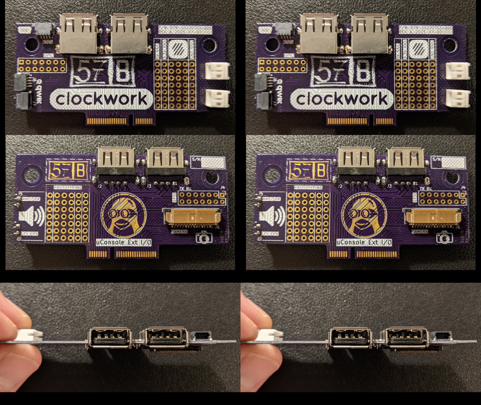
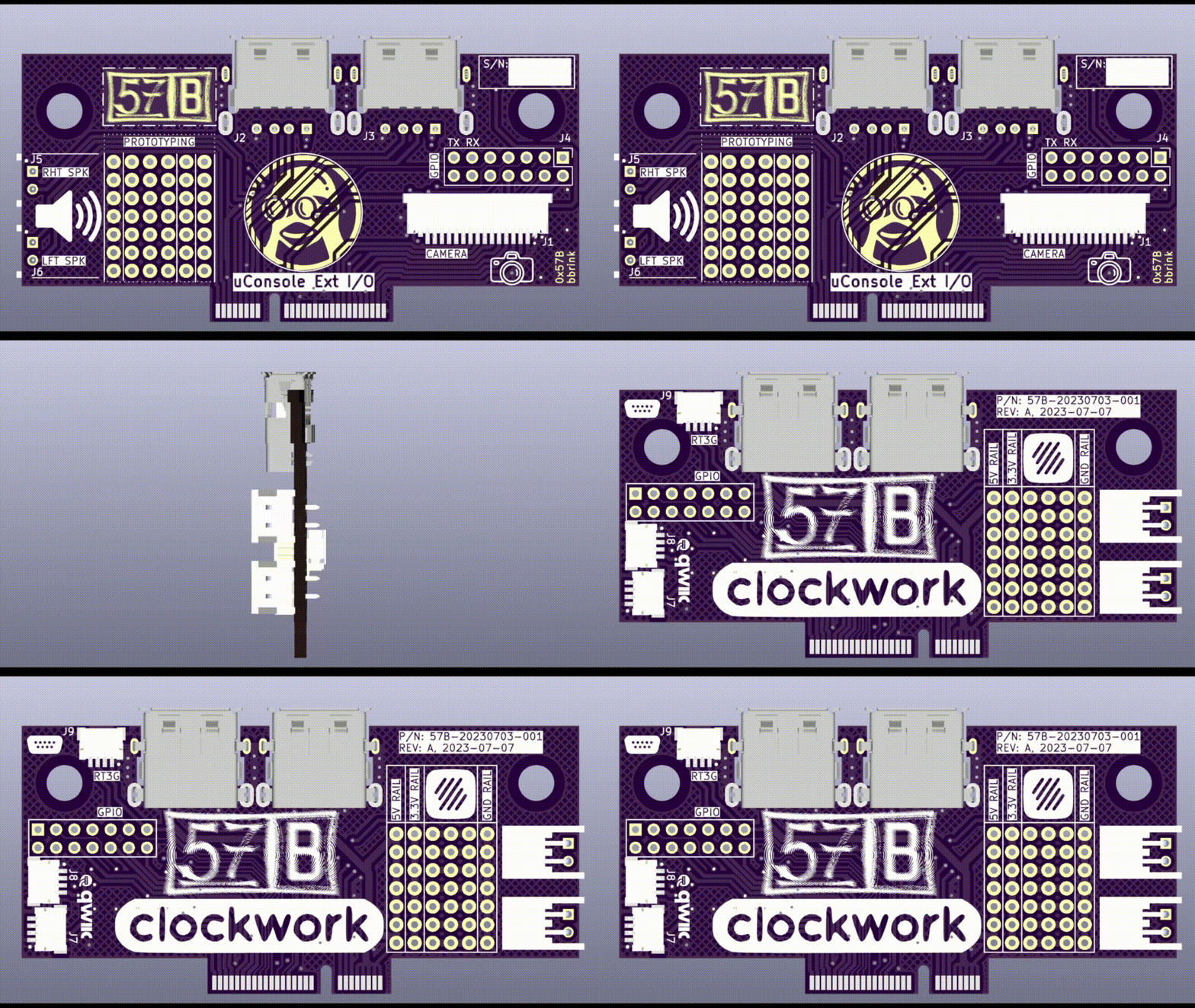
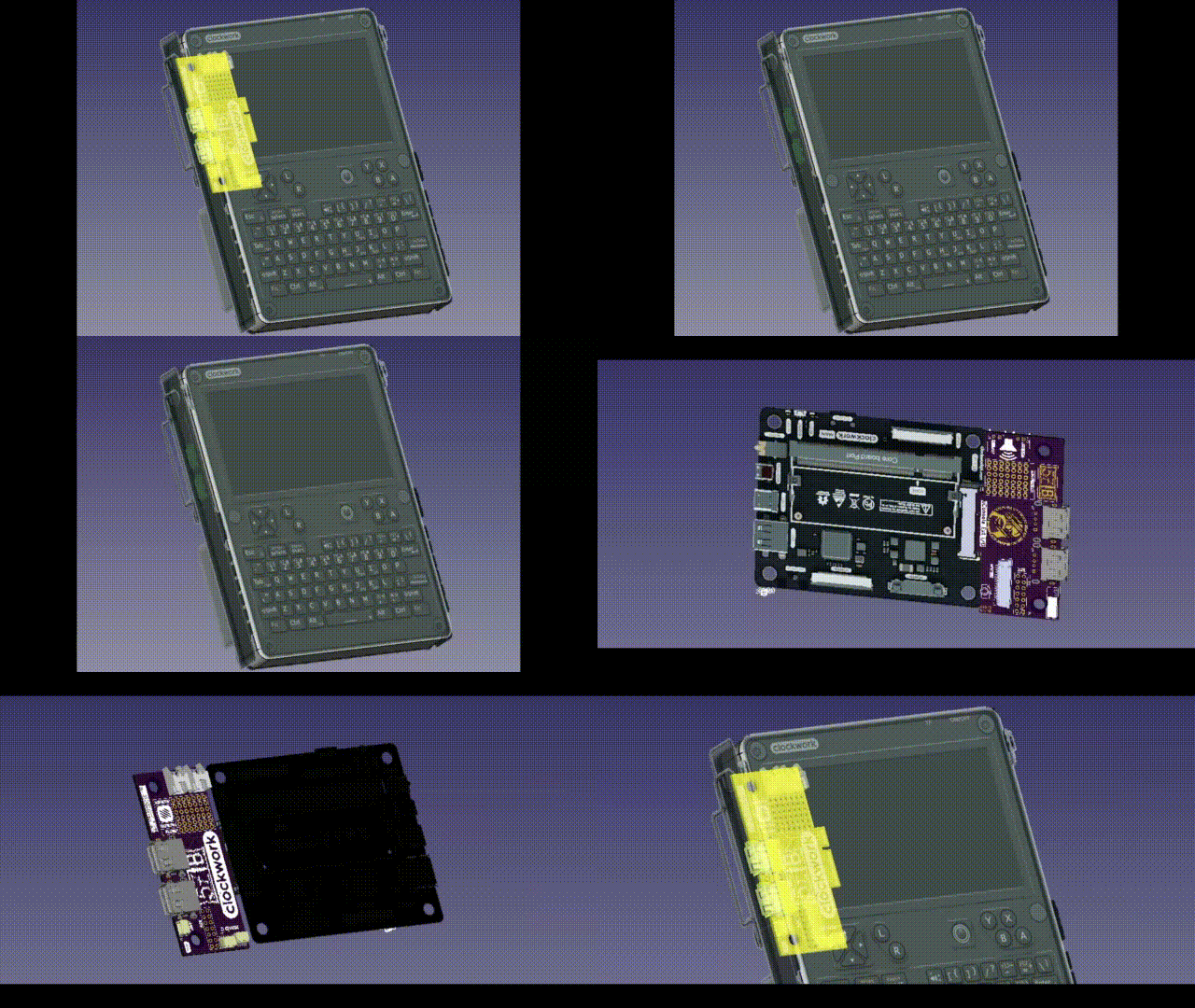
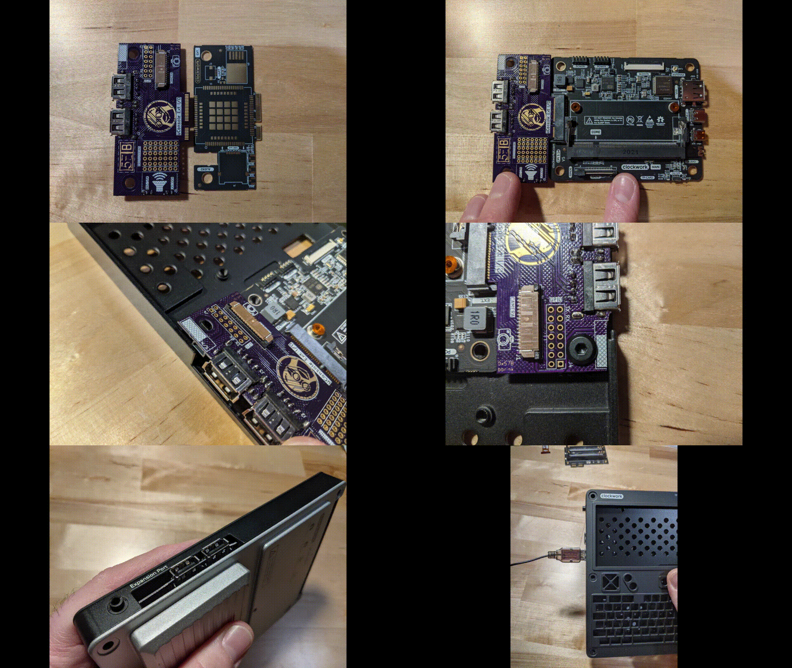
Epic fail on REV: A.
When I made it, CPI hadn't released the DXF for the 4G card yet. I had to eyeball the board outline based on the website images. I missed the outer edge by 1mm.
Luckily the edge was just ground plane, and I was able to file the FR4 back to get it to fit. Continuity checks out, but.... I think a REV: B is in order ha.
The fixes for REV: B are:
| Qty | Value | Footprint | References |
|---|---|---|---|
| 9 | LOGO | LOGO | G***, G***, G***, G***, G***, G***, G***, G***, G*** |
| 3 | SM04B-SRSS-TB(LF)(SN) | 1_project:JST_SM04B-SRSS-TB(LF)(SN) | J7, J8, J9 |
| 2 | GSB12J21C1EU | 1_project:GSB12J21C1EU | J2, J3 |
| 2 | S2B-XH-A(LF)(SN) | 1_project:JST_S2B-XH-A(LF)(SN) | J5, J6 |
| 1 | Conn_02x07_Counter_Clockwise | Connector_PinHeader_2.54mm:PinHeader_2x07_P2.54mm_Vertical | J4 |
| 1 | SFW15R-2STE1LF | 1_project:AMPHENOL_SFW15R-2STE1LF | J1 |
| 1 | ~ | 1_project:ext_card_fp | P1 |
The 19 most common of 25 parts.
ben5049/Keyboard
Features: - Wireless - 900mAh battery - Bluetooth (nRF52) - ZMK - 4 Port USB hub - BLDC Knob for haptic feedback - Kailh Choc V1 switches


RobertLukan/rpi-cm4-custom-board
Based on my previous projects I needed a customized RPI4 carrier board with 2 cameras input. The initial idea was taken from this project…


thingino/teacup-neo
Universal Ingenic SoC development platform: one carrier + per-SoC interposer modules (T10 through A1, any package) on a DDR4 card edge, with an ESP32-S3 BMC for autonomous LLM-driven development.

Mimoja/RPI5-DSI-ST7701-Adapter
An adapter board for DSI boards that have direct LED connection and need a reset pin

ngrabbs/ember
Open pvpanel.kicadpro with KiCad 10. The project contains the recovered schematic, routed PCB, project-local footprint libraries, and solar-module STEP model.
It measures 78 × 37.5 mm and has 2 copper layers, 1.6 mm thick.
25 parts, built around the SM04B-SRSS-TB(LF)(SN), GSB12J21C1EU, S2B-XH-A(LF)(SN) and SFW15R-2STE1LF. The full list of its parts is on this page, with links to each part's symbol and footprint where PCBKit's library has them.
From the 57Bravo/uConsole_Ext_IO_Breakout repository on GitHub, at the commit this page was made from: the board is pcb/ext_pcb/ext_pcb.kicad_pcb and its schematic pcb/ext_pcb/ext_pcb.kicad_sch. PCBKit opens the board in the browser, with nothing to install.
Its repository states no licence, so its author keeps all rights: ask 57Bravo before reusing the design.