4 layers54 × 120 mm
Kartonaut
Jan-Philipp-Munsch/kartonaut
TVC model rocket (after BPS.space Scout F): Teensy 4.1 flight firmware, mainboard spec, project log
174 partsMIT

 3amon/leaderless-light-mesh
Wearable LED rings that keep a shared clock with no leader: Zephyr/OpenThread firmware, signed OTA, carrier PCB, simulators and hardware evidence
Thread led node is an open-source printed circuit board by 3amon, from the 3amon/leaderless-light-mesh repository on GitHub, published under the MIT licence. It is a 2-layer board of 80 × 46 mm with 24 parts on 13 nets, routed with 70 tracks and 32 vias.
It is built around the SN74LV1T34DBVR-TP and AO3401A. Its parts include 5 resistors, 4 connectors, 2 capacitors, 2 transistors and 1 IC.


KiCad 10 project for an 80 x 46 mm, 2-layer carrier that takes a SuperMini
nRF52840 module (a nice!nano-style "Pro Micro nRF52840" clone) and drives an
external WS2812B ring or strip. Design files are CC BY 4.0
(../LICENSE-hardware.md).
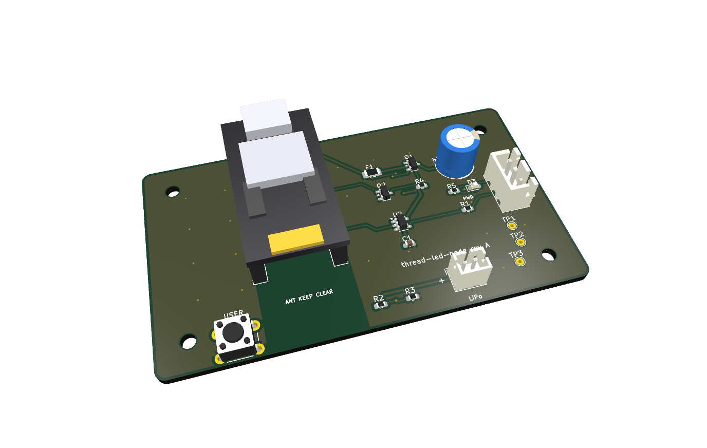
Rev A has two known errors. Read
../docs/hardware-rev-a-errata.mdbefore building one.
- The module has 13 positions per side (separate B-/B+ pins at the USB end); the carrier was laid out with 12-position sockets. Seat the module with B-/B+ hanging outside the sockets. Seating them in the sockets shifts every pin by one and shorts RAW to ground.
- J2+ is routed to RAW rather than the module's B+ charger terminal. Do not connect a rechargeable battery to J2. USB and current-limited bench power are verified; battery operation is not safe on Rev A.
The silkscreen pin labels also print partly off the board edge.
| Path | Contents |
|---|---|
thread-led-node.kicad_sch, .kicad_pcb, .kicad_pro | Schematic, board, project |
gerbers/ | Gerbers and Excellon drill files as sent to the fab |
assembly/ | BOM and placement (CPL) files for JLCPCB assembly |
fab_export.py | Regenerates the fab package; computes placement centroids from pad bounding boxes and applies per-footprint rotation offsets (why: see ../docs/kicad-notes.md) |
models/supermini_nrf52840.wrl | Generated box-model stand-in for the module, used for the 3D render |
renders/ | 3D render, top view (PNG and SVG) |
thread-led-node.kicad_pcb.drc.json | KiCad DRC report: 0 errors, 5 warnings (silkscreen), 0 unconnected |
fab_export.py needs KiCad's pcbnew Python module and kicad-cli. Footprints
and 3D models come from the stock KiCad libraries, which are not redistributed
here.
EN_LED (P0.17) high before the LED rail is live, wait
for it to settle, and send black before turning it off.| Signal | Pin | Board net |
|---|---|---|
| LED data out | P0.06 (J3-1) | LED_DATA_MCU -> U2 -> 330 ohm -> J1-2 |
| LED power enable | P0.17 (J3-5) | EN_LED (high = strip on) |
| USER button | P0.20 (J3-6) | BTN (to GND, internal pull-up) |
| Battery sense | P0.31 / AIN7 (J4-5) | VBAT_DIV. Measured floating on the tested modules: see the errata |
| Ref | Part | LCSC |
|---|---|---|
| U2 | SN74LV1T34DBVR, SOT-23-5 | C100024 |
| Q1 | AO3401A P-FET, SOT-23 | C15127 |
| Q2 | 2N7002, SOT-23 | C8545 |
| F1 | 1206L110THYR polyfuse 1.1 A | C126818 |
| J1 | JST B3B-XH-A 3-pin | C144394 |
| J2 | JST-PH 2-pin | C126363 |
| J3, J4 | 1x12 2.54 mm female header | C7509522 |
| C1 | 100 nF 0603 | C14663 |
| C2 | 470 uF 16 V radial | C105296 |
| R1 | 330 ohm 0603 | C23138 |
| R2, R3 | 1 M 0603 | C22935 |
| R4 | 100 k 0603 | C25803 |
| R5 | 1 k 0603 | C21190 |
| D3 | red LED 0603 | C2286 |
| SW1 | 6x6 mm THT tactile | C42416242 |
Recorded cost for five assembled boards: PCB $2 + assembly $28.52, before
shipping (../docs/kicad-notes.md).
| Qty | Value | Footprint | References |
|---|---|---|---|
| 4 | MountingHole_2.7mm | MountingHole_2.7mm | MH1, MH2, MH3, MH4 |
| 3 | TestPoint_THTPad_D1.5mm_Drill0.7mm | TestPoint_THTPad_D1.5mm_Drill0.7mm | TP1, TP2, TP3 |
| 2 | 1M | Resistor_SMD:R_0603_1608Metric | R2, R3 |
| 1 | 1.1A | Fuse:Fuse_1206_3216Metric | F1 |
| 1 | 100k | Resistor_SMD:R_0603_1608Metric | R4 |
| 1 | 100nF | Capacitor_SMD:C_0603_1608Metric | C1 |
| 1 | 2N7002 | Package_TO_SOT_SMD:SOT-23 | Q2 |
| 1 | 330 | Resistor_SMD:R_0603_1608Metric | R1 |
| 1 | 470uF | Capacitor_THT:CP_Radial_D8.0mm_P3.50mm | C2 |
| 1 | AO3401A | Package_TO_SOT_SMD:SOT-23 | Q1 |
| 1 | LED_0603_1608Metric_Pad1.05x0.95mm_HandSolder | LED_0603_1608Metric_Pad1.05x0.95mm_HandSolder | D3 |
| 1 | LiPo_1S | Connector_JST:JST_PH_B2B-PH-K_1x02_P2.00mm_Vertical | J2 |
| 1 | R_0603_1608Metric | R_0603_1608Metric | R5 |
| 1 | SN74LV1T34DBVR | Package_TO_SOT_SMD:SOT-23-5 | U2 |
| 1 | SuperMini_L | Connector_PinSocket_2.54mm:PinSocket_1x12_P2.54mm_Vertical | J3 |
| 1 | SuperMini_R | Connector_PinSocket_2.54mm:PinSocket_1x12_P2.54mm_Vertical | J4 |
| 1 | USER | Button_Switch_THT:SW_PUSH_6mm | SW1 |
| 1 | WS2812B_OUT | Connector_JST:JST_XH_B3B-XH-A_1x03_P2.50mm_Vertical | J1 |
It measures 80 × 46 mm and has 2 copper layers, 1.6 mm thick.
24 parts, built around the SN74LV1T34DBVR-TP and AO3401A. The full list of its parts is on this page, with links to each part's symbol and footprint where PCBKit's library has them.
From the 3amon/leaderless-light-mesh repository on GitHub, at the commit this page was made from: the board is hardware/thread-led-node.kicad_pcb and its schematic hardware/thread-led-node.kicad_sch. PCBKit opens the board in the browser, with nothing to install.
Its repository publishes it under the MIT licence: you may reuse it on that licence's terms (keep the author's notice, and for a copyleft licence share your changes alike).
Jan-Philipp-Munsch/kartonaut
TVC model rocket (after BPS.space Scout F): Teensy 4.1 flight firmware, mainboard spec, project log


brenocq/bldc-motor
High-precision BLDC motor and controller development from scratch (in progress...)


YuuichiAkagawa/USBMIDItoSyncConverter
Converts USB MIDI clock messages to sync signals

