
4 layers62.1 × 83.8 mm
Ss main board
loopj/short-stack
World's Smallest Nintendo Wii, using a trimmed motherboard and custom stacked PCBs
69 parts804

 19AJ137/SiliCa47
FeliCa®互換カード「SiliCa」
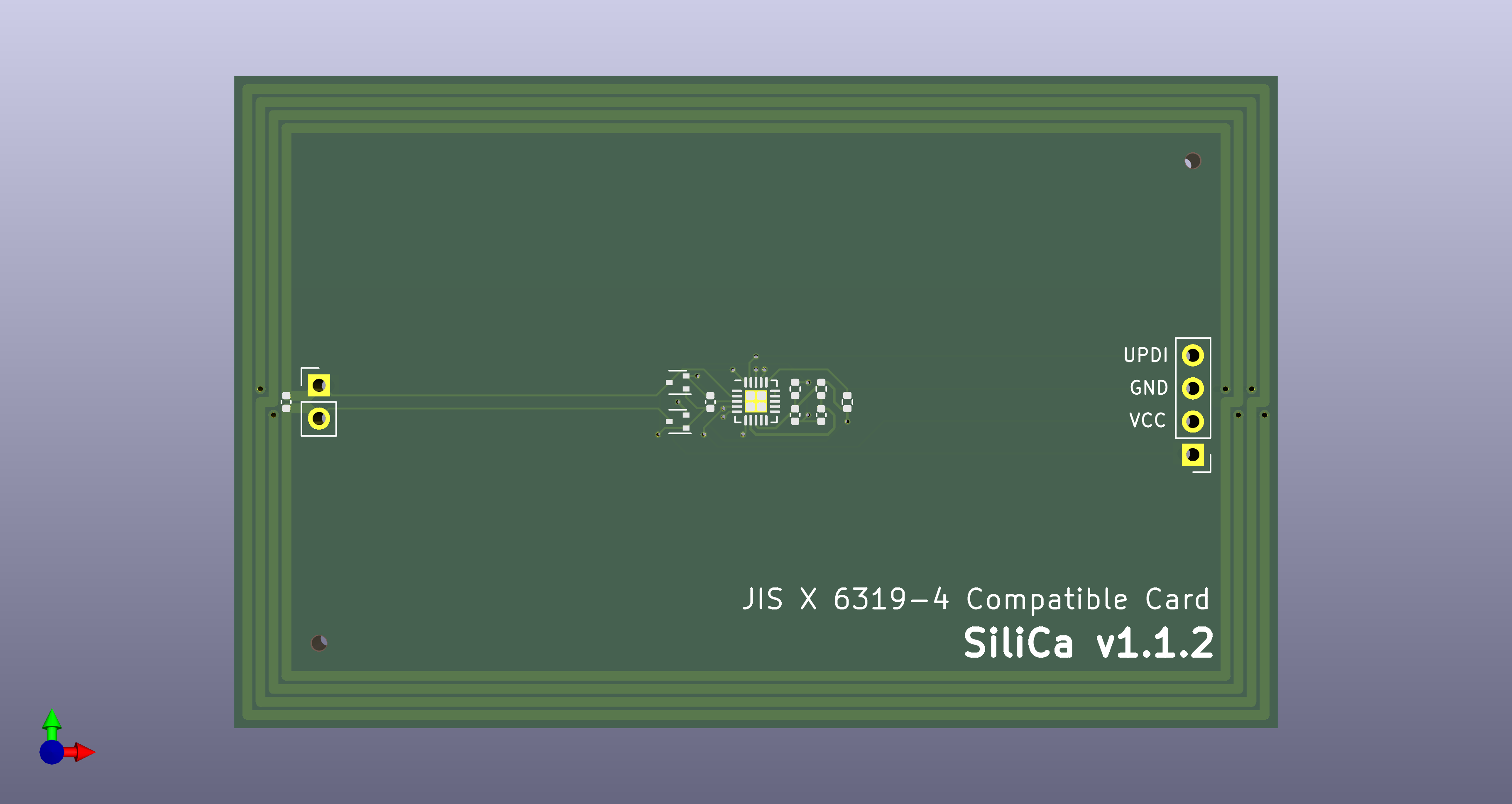
SiliCa is an open-source printed circuit board by 19AJ137, from the 19AJ137/SiliCa repository on GitHub, published under the Unlicense licence. It is a 2-layer board of 80 × 50 mm with 14 parts on 17 nets, routed with 145 tracks and 20 vias.
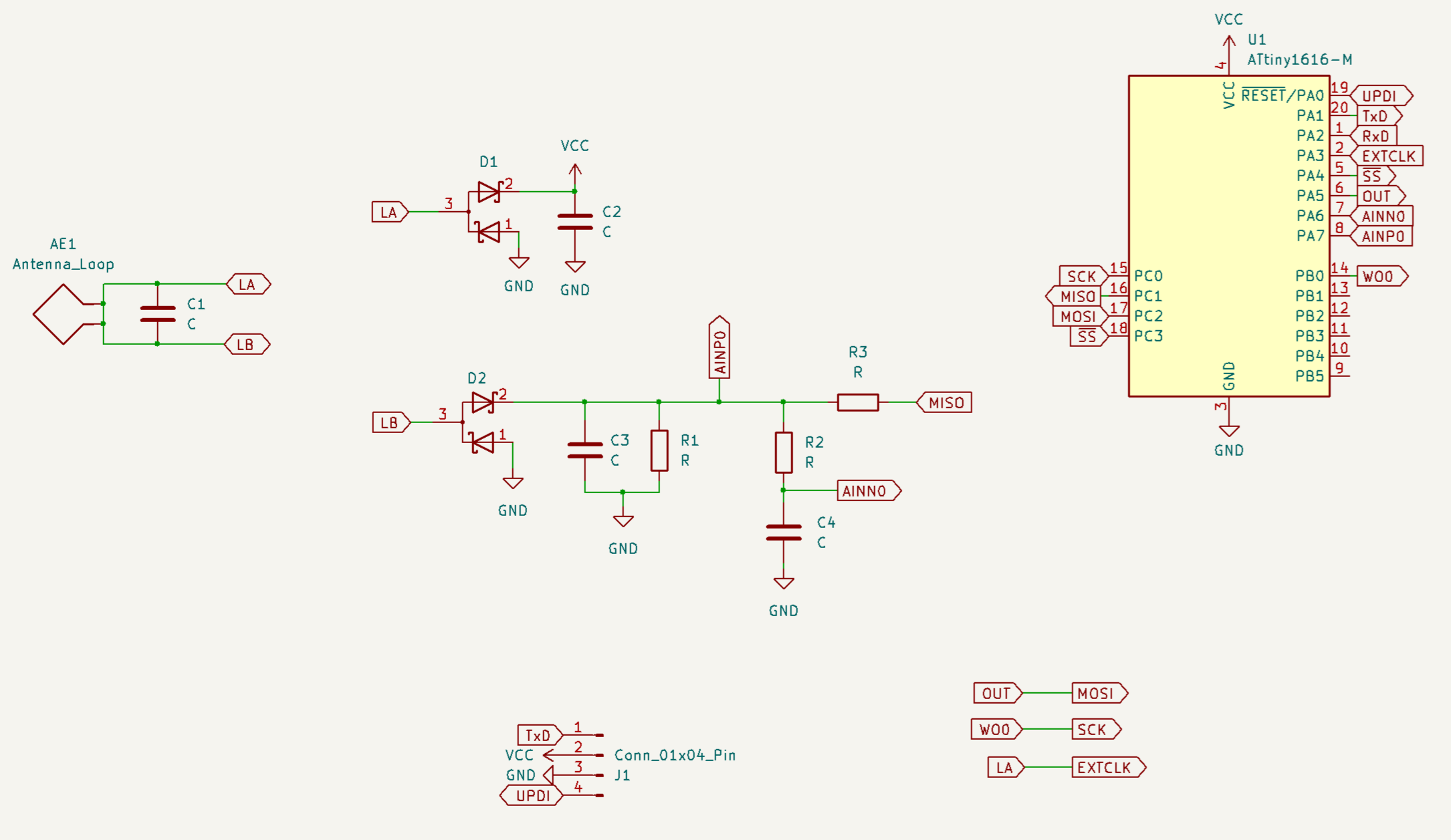
It is built around the ATTINY1616-MN. Its parts include 4 capacitors, 3 resistors, 2 diodes, 1 IC and 1 connector. It belongs with the radio and wireless boards and the AVR (ATmega, ATtiny) boards of this library.
SiliCa は、JIS X 6319-4(FeliCa)互換の非接触型 IC カードです。
マイコンとして ATtiny1616 を採用しており、外部電源を必要とせず、カードリーダからの給電によって動作します。
SiliCa は、最小限のハードウェア構成で、 FeliCa プロトコルをファームウェアによって再現し、FeliCa Standard や FeliCa Lite-S のエミュレーションを実現することを目的としています。
また、SiliCa では、実際の FeliCa カードで書き換えが不可能な IDm やシステムコードなどのパラメータを自由に書き換えることができます。
詳細な仕様や使用方法については、寄稿した同人誌 rand_r(&v3) をご参照ください。
本プロジェクトは、学術的および実験的な目的で提供されており、商業利用や実際の運用を目的としたものではありません。
FeliCaは、ソニー株式会社が開発した非接触ICカードの技術方式です。
FeliCaは、ソニーグループ株式会社の登録商標です。
本文では™、®は明記していません。| Qty | Value | Footprint | References |
|---|---|---|---|
| 4 | C | Capacitor_SMD:C_0402_1005Metric | C1, C2, C3, C4 |
| 3 | R | Resistor_SMD:R_0402_1005Metric | R1, R2, R3 |
| 2 | D_Schottky_Dual_Series_AKC_Parallel | Package_TO_SOT_SMD:SOT-523 | D1, D2 |
| 1 | ATtiny1616-M | Package_DFN_QFN:VQFN-20-1EP_3x3mm_P0.4mm_EP1.7x1.7mm | U1 |
| 1 | Antenna_Loop | Connector_PinHeader_2.54mm:PinHeader_1x02_P2.54mm_Vertical | AE1 |
| 1 | Conn_01x04_Pin | Connector_PinHeader_2.54mm:PinHeader_1x04_P2.54mm_Vertical | J1 |
The 12 most common of 14 parts.
loopj/short-stack
World's Smallest Nintendo Wii, using a trimmed motherboard and custom stacked PCBs


kieraneglin/hexagon-art
A passive breakout board: two lever-terminal inputs, three JST XH outputs, all six conductors (RX bus, two spares, +12V, GND, +5V) paralleled straight across. No active components, no regulation, nothing to configure.

engineerbo/flashlight-dev-hw
This repository contains design files for the development board for a flashlight boost driver. The test firmware can be found in the firmware repository.

hojadurdy/Flux_Capacitor_Micro
A tiny (36mm x 29mm) pin badge and keychain PCB version of Flux Capacitor featuring 25 animated LEDs that animate to create the “fluxxing” effect.


MertX2/PowerStripHavoc
Its name is a combination of loopj's PowerStrip, which is the base of this project, and the Havoc weapon from Apex Legends.
It measures 80 × 50 mm and has 2 copper layers, 1.6 mm thick.
14 parts, built around the ATTINY1616-MN. The full list of its parts is on this page, with links to each part's symbol and footprint where PCBKit's library has them.
From the 19AJ137/SiliCa repository on GitHub, at the commit this page was made from: the board is cad/1_1/1_1.kicad_pcb and its schematic cad/1_1/1_1.kicad_sch. PCBKit opens the board in the browser, with nothing to install.
Its repository publishes it under the Unlicense licence: you may reuse it on that licence's terms (keep the author's notice, and for a copyleft licence share your changes alike).