4 layers150 × 120 mm
Ephys test board
open-ephys/ephys-test-board
General purpose, automated electrophysiology test board
567 parts1

 zmcginty/OpenTMS20
Open-Source Transcranial Magnetic Stimulator. High energy pulse circuitry, simple controllers, and coil design.
TMS IGBT And Gate Drive is an open-source printed circuit board by zmcginty, from the zmcginty/OpenTMS repository on GitHub. It is a 2-layer board with 42 parts on 35 nets, routed with 21 tracks and 0 vias.
It is built around the IRG4PF50WPBF, ADS1115IDGS and MCP1415-E/OT, with the AD5683RARMZ and LM293DR among its other parts. Its parts include 12 resistors, 9 ICs, 3 capacitors and 1 transistor.


An open-source transcranial magnetic stimulator (TMS) project, including coil designs, pulse-generator hardware, and control/charging circuitry.
Safety Notice This is not a legitimate medical device and is not a substitute for real TMS treatment. This is an experiment I built in my garage, and I cannot verify that it does what it's supposed to (if anyone wants to build an open-source MRI.... let me know...) This device is dangerous, it operates at energy levels more than enough to stop your heart, kill you, blow up and do lots of damage. If you're going to play with high energy pulsed power systems; be careful.
I primarily build two coil geometries — single coils and figure-8 coils. What I've focused on are air-core windings in either single-layer or multi-layer form. The general architecture is adapted from research papers and the limited information published by commercial TMS coil manufacturers. The figure-8 CloudTMS coil (below) was a major influence on my designs in terms of hollow copper conductor carrying coolant.
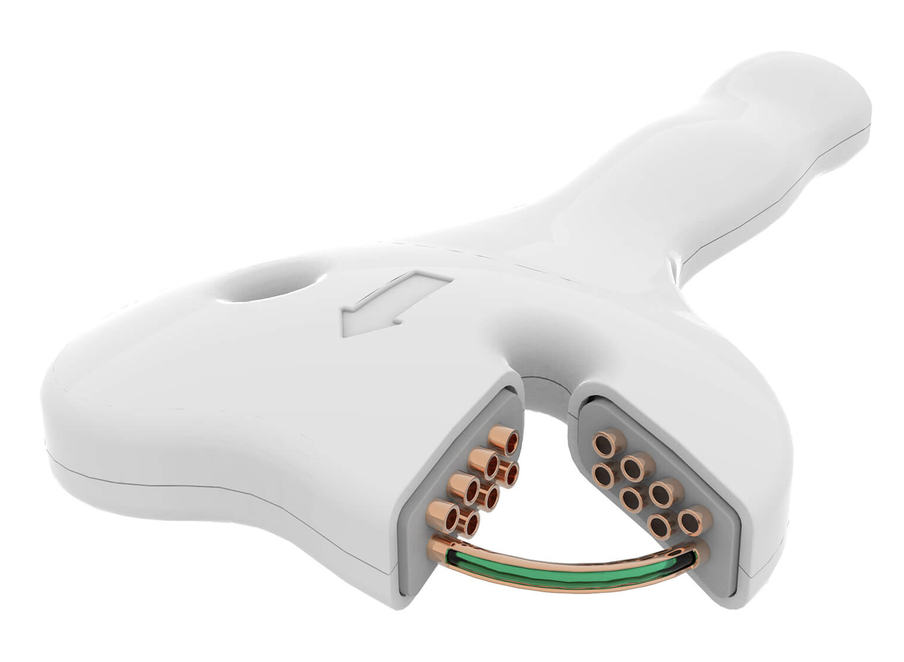
As I moved to higher pulse rates and energies, active cooling became necessary. My preferred approach, similar to the CloudTMS design, uses hollow copper tubing (sold for HVAC/refrigeration) insulated with PTFE heat-shrink. PTFE works well because it's a good dielectric, stays thin-walled after shrinking, tolerates high temperatures, and holds the coil shape better than thicker heat-shrink alternatives — though it does require fairly high heat to shrink fully.
Build process:
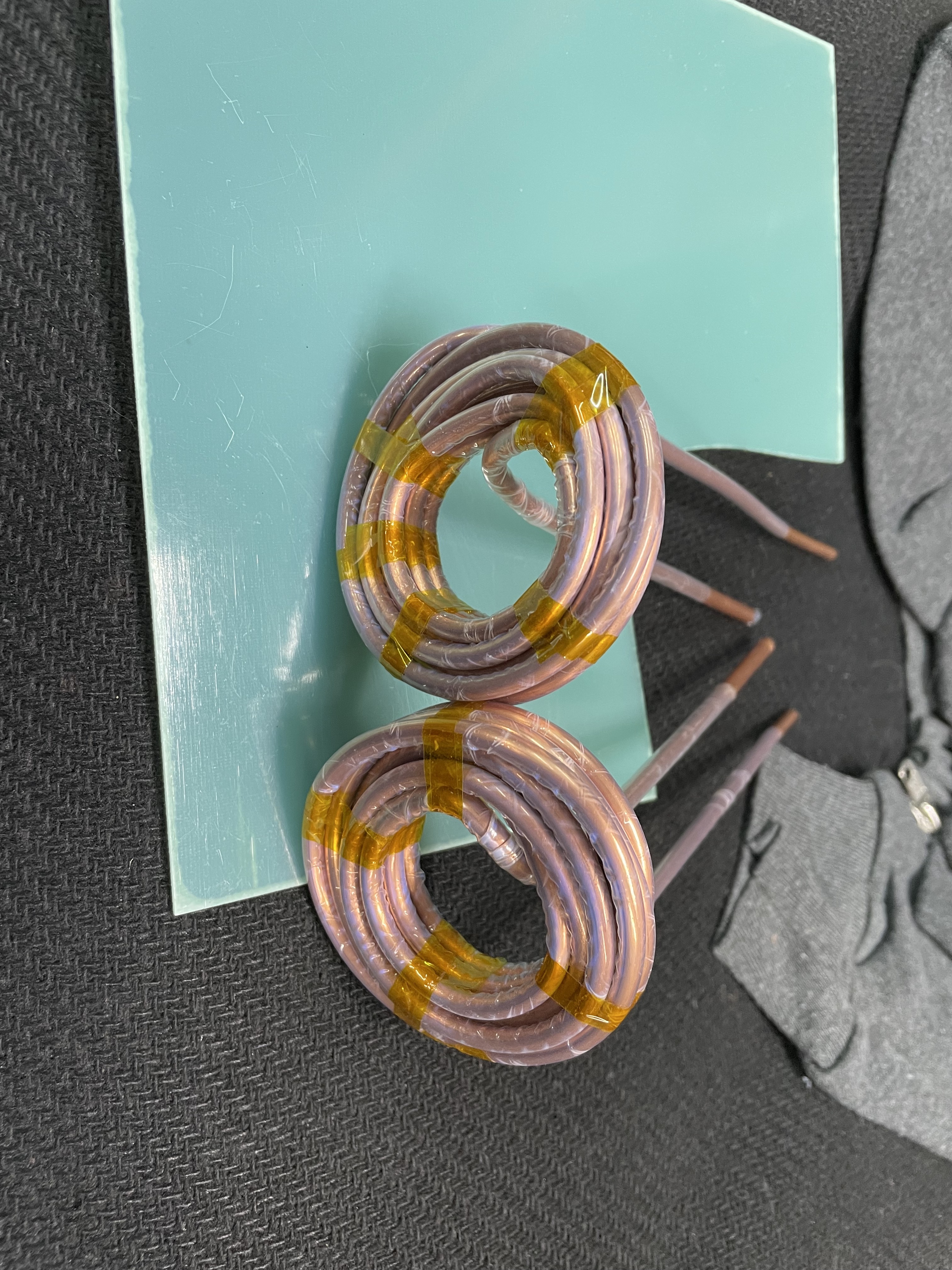
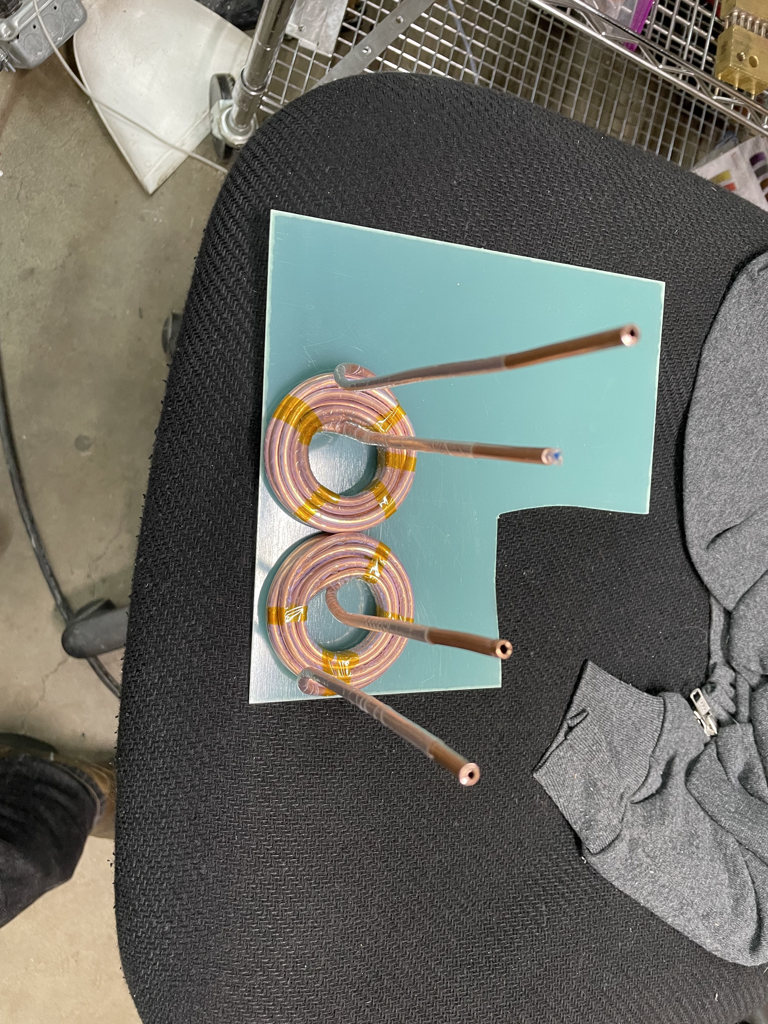
Example coil before potting
Potting the coil in epoxy significantly improves mechanical stability and reduces noise by keeping the windings from moving against each other under pulse forces. Hot glue works as an alternative but produces coils that are noticeably louder in operation — not confidence-inspiring at higher power levels.
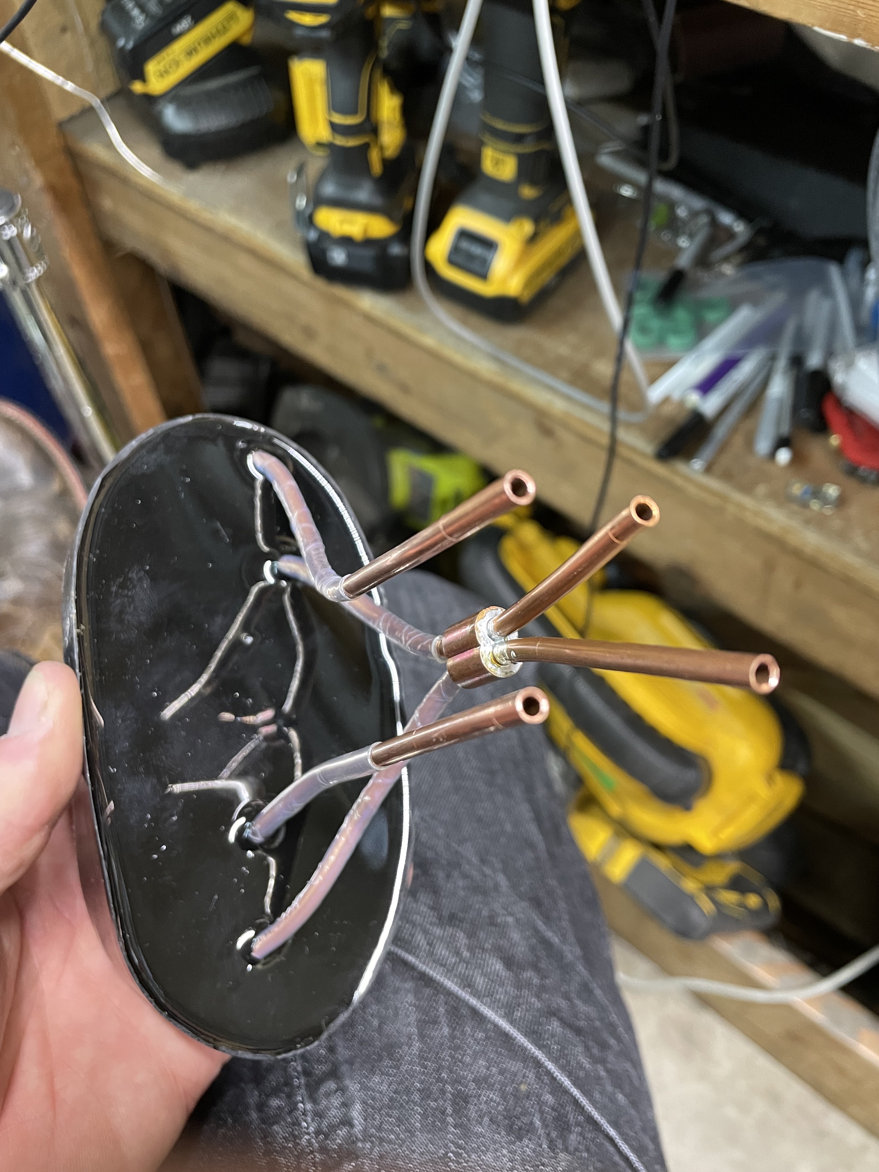
Example coil after potting
Coils built from hollow copper tube are cooled by pumping coolant through the winding itself.
| Material | Purpose | Notes |
|---|---|---|
| Hollow copper tube | Water-cooled coil winding | Standard refrigeration-grade tube; cheap and widely available |
| Fiberglass resin sheet | Application-side coil face | Sturdy, good electrical insulator, and appears permeable to magnetic fields — a disassembled commercial coil used what looked like FR4 fiberglass (PCB-grade) |
| MAX EPC epoxy potting compound | Coil potting | Inexpensive, good electrical insulator, decent thermal conductivity. For tube-cooled coils, MAX MCR (lower thermal conductivity) is also an option |
My current switch of choice is the Infineon/Eupec FZ1200R33KF2 — inexpensive and capable of handling substantial power. Prices on eBay range from ~$100–$400, and I've pushed 8kA pulses through a single unit. Adequate snubber capacitance/circuitry is essential to keep the voltage across the device under its 3.3kV rating (I target a safety margin below that).
I've used two Power Integrations gate drivers with this IGBT:
Monitoring Vce (collector-emitter voltage) across each IGBT is critical to staying within its rating — I keep a safety margin and stay below 2.5kV on 3.3kV-rated devices. Since these switches operate on the high side, measurement requires a high-voltage differential probe: I use a Micsig DP20003 (5600V, 100MHz). A similar, lower-range HV differential probe (1300V) monitors the main capacitor bank voltage.
A shunt resistor was my first attempt but never produced a trustworthy signal. Two methods have worked well since:
The charging circuit is a simple, open-loop design: mains power feeds a variable transformer (variac), which drives a microwave oven transformer (MOT) to step up voltage. The stepped-up AC is rectified by a full-bridge rectifier and used to charge the main discharge capacitor bank, which is then discharged through the coil via a high-side switch (latching SCR or non-latching IGBT).
The current two-switch flyback pulse generator uses two matched MOTs (matched by checking voltage and phase agreement between units — measurements/resources TODO). Drawing ~15A at 120V, two matched transformers stay below ~60°C with air cooling alone.
Earlier designs used a single MOT with low-pressure mineral-oil cooling, which worked up to ~14A — but oil cooling systems and pumps added complexity and were prone to leaks.
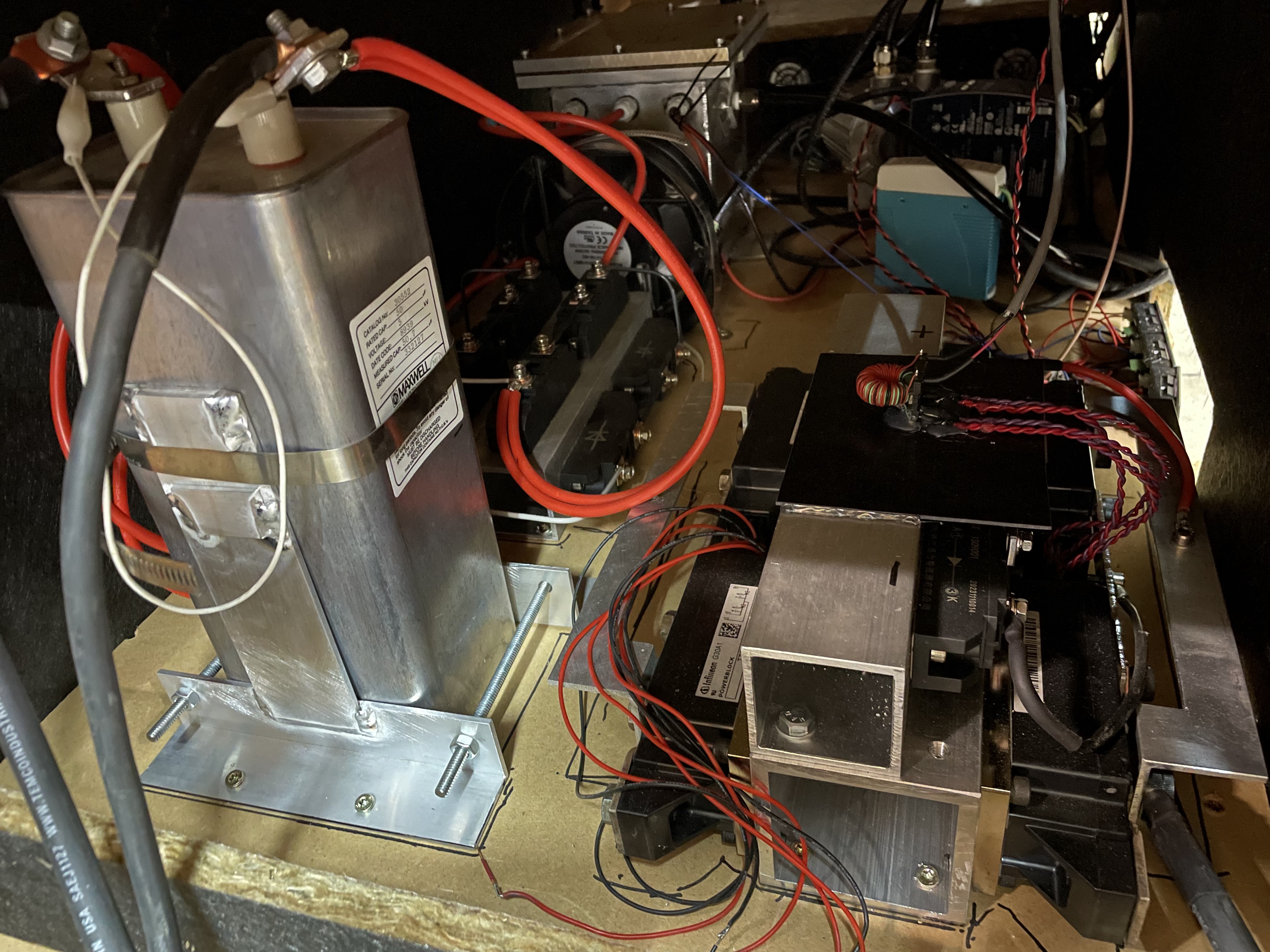
SCR-switch pulse generator (SCRs are bottom-right. Main capacitor front left. Rectifier behind capacitor. and mineral-oil cooled microwave transformer behid rectifier.
The first design I built. It handles very high energy levels well at consistent frequencies/patterns (e.g., the standard 5Hz/10Hz protocols used in early depression-treatment research). Its limitation is pattern flexibility: an SCR/thyristor is a latching switchable diode, so once triggered it fully discharges the capacitor. This steady current decay is gentle on flyback effects but rules out more complex patterns like Theta-Burst (50Hz bursts repeating at 4–5Hz).
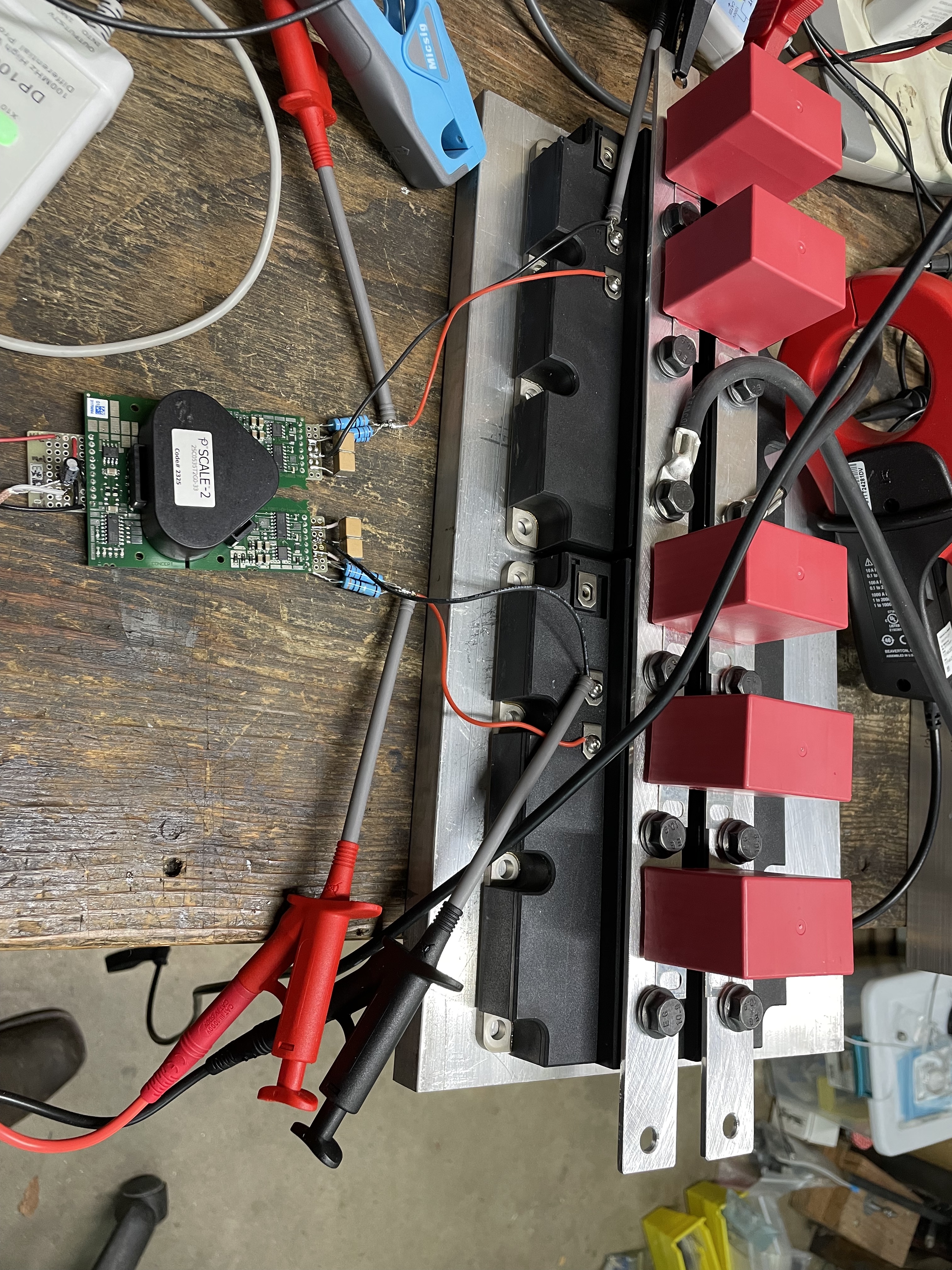
Single IGBT topology (note; two IGBTs in parallel), you can also see gate driver I used before using ones built specifically for the IGBT module
Since IGBTs aren't latching, they can be switched on and back off within a short pulse, allowing partial capacitor discharge and enabling patterns like Theta-Burst. The tradeoff is significant flyback voltage when interrupting current through the coil — this destroyed several IGBTs before I addressed it with a robust flyback diode across the coil and snubber capacitors across the IGBT(s) to absorb spikes from parasitic wiring/busbar inductance. HV differential probes are essential here to stay within the switch's voltage rating while tuning.
This design uses a flyback diode across the coil, producing a sharp current rise but a slow fall (as flyback energy dissipates through coil/wire resistance and the diode). It worked well and was relatively simple compared to the two-switch flyback design, but since flyback energy isn't recycled, it's ultimately limited by the 120V/15A charging circuit.
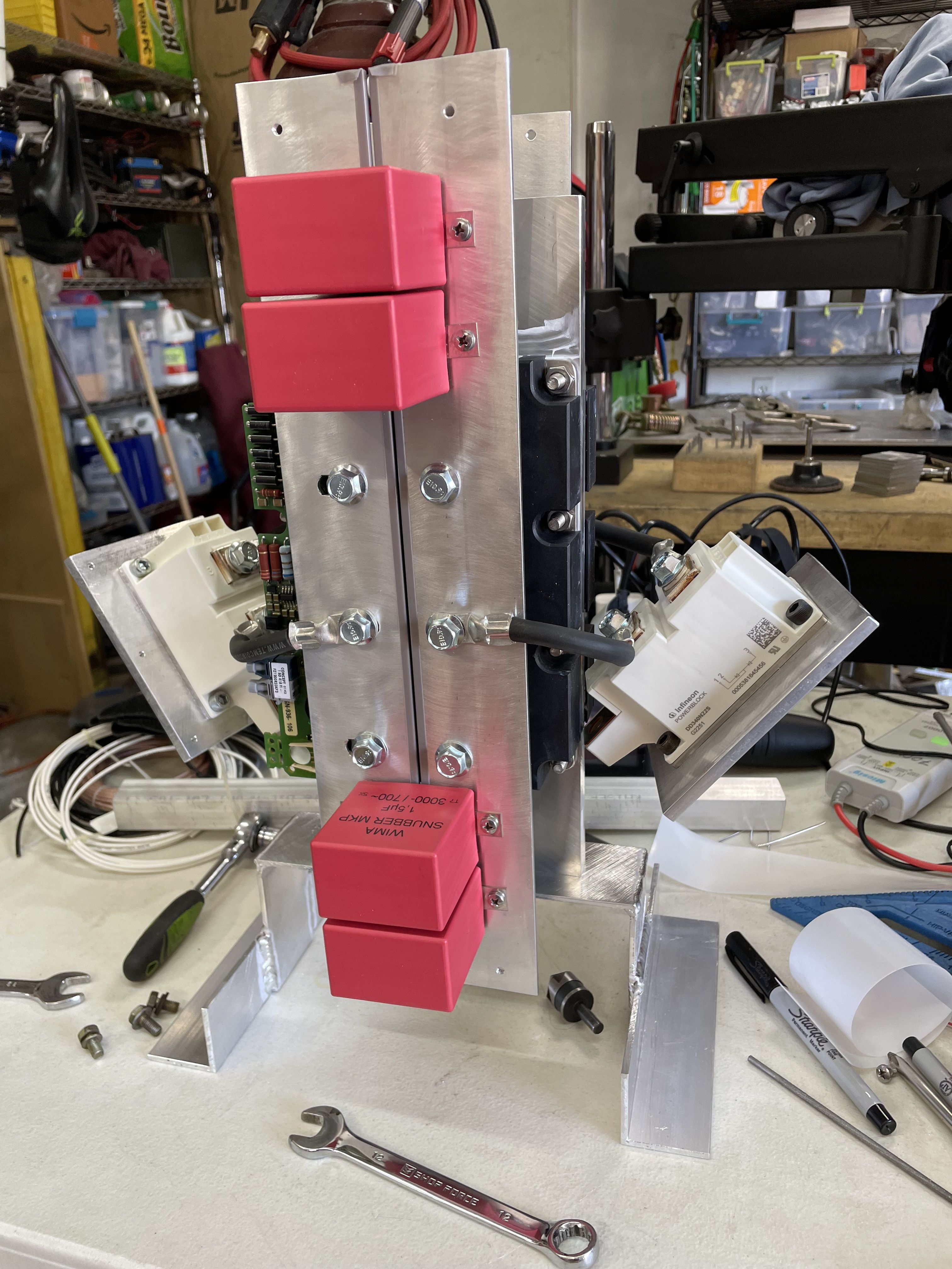
Two-Switch flyback topology being built. You can see the diodes hanging off to the sides. And gate drives are now on the left, bolted to IGBT modules behind bus-bars.
This design recycles more pulse energy than the single-IGBT version and produces both a sharp rising and falling current edge, increasing di/dt for a stronger but shorter magnetic field pulse. It noticeably reduced charging-circuit current draw and appears more effective at stimulating muscle/nerve tissue than the single-switch design, even at higher peak current — likely because faster field transitions induce greater current in tissue.
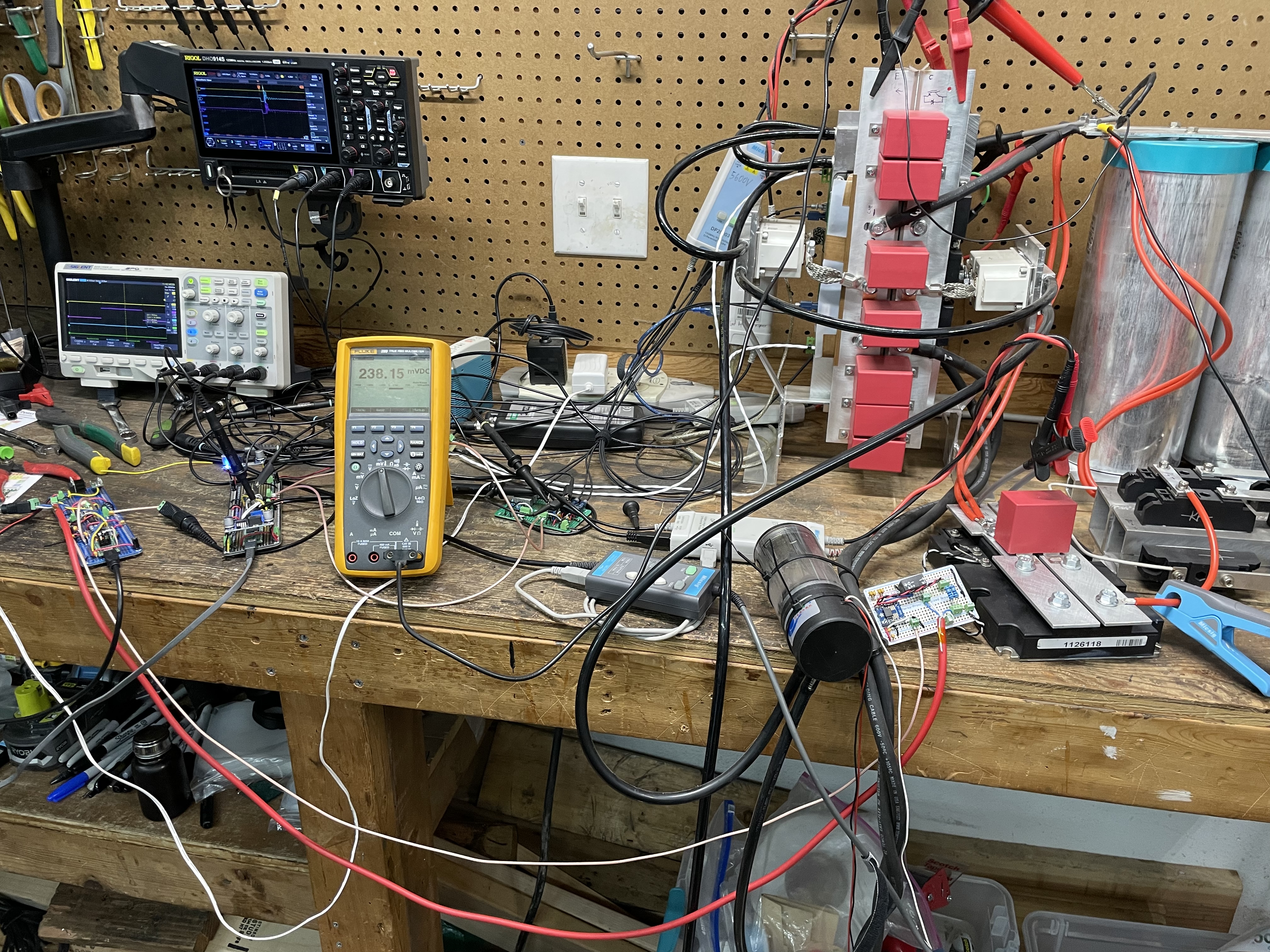
Photo of the system, from left-to-right; charge-control board, multimeter, main pulse-IGBTs (with many red snubber caps), charge-control IGBT (with single red snubber in front), charge-circuit-rectifier, and main pulse capacitor bank in back
Should double coil pulse current relative to the two-switch flyback topology by enabling current reversal. The complexity of positioning four large IGBT switches and the associated snubbers and diodes close to eachother, with cooling is going to be difficult without adding parasitic inductance that would offset the gains.
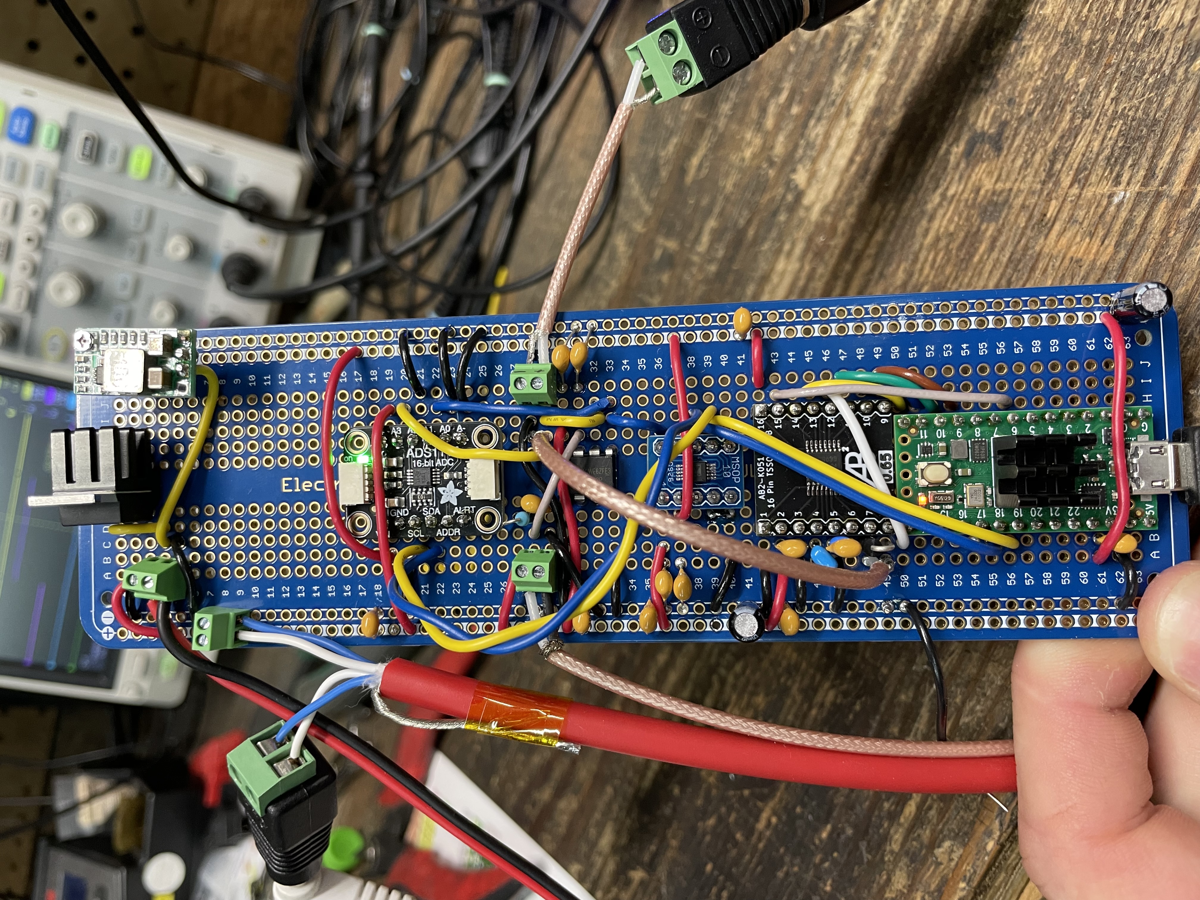
Newly Built Charge-Control Board with (from bottom to top) Teensy 4.0, ADS8699 high-speed ADC, AD5693 DAC, LM393P Comparator, ADS1115 4ch slow ADC, 5V LDO, and 3.3V buck-converter
The new charge-control system seems to be working well enough for calling it version 1!!! After many failed attempts to measure a voltage divider, and my ground plane shifting and making either the teensy and/or ADC shit itself, even after adding digital SPI isolators, I realized.... that's what HV diff probes are for! So ripped out some HV SPI/I2C isolators and I'm now just measuring the output of a Micsig 1300v diff probe. No glithes, no isolators causing signal delays, no fried chips and salsa. Perfect.
The new approach uses a DAC to output a reference voltage into a comparator, which compares it against the output of the Micsig 1300v differential probe. I have probe scale-factors in the teensy code as well as linear calibrations for both ADCs and DAC as well. I have the fast ADC on here as well incase I want to control the charge-circuit via the teensy reading ADC instead of from the comparator + DAC, but for now the comparator + DAC method is working great, so we have some extra/redundant ADCs. A weak pull-down on the DAC output ensures that if the microcontroller glitches or crashes, the DAC voltage falls to zero and the charge circuit fails safely.
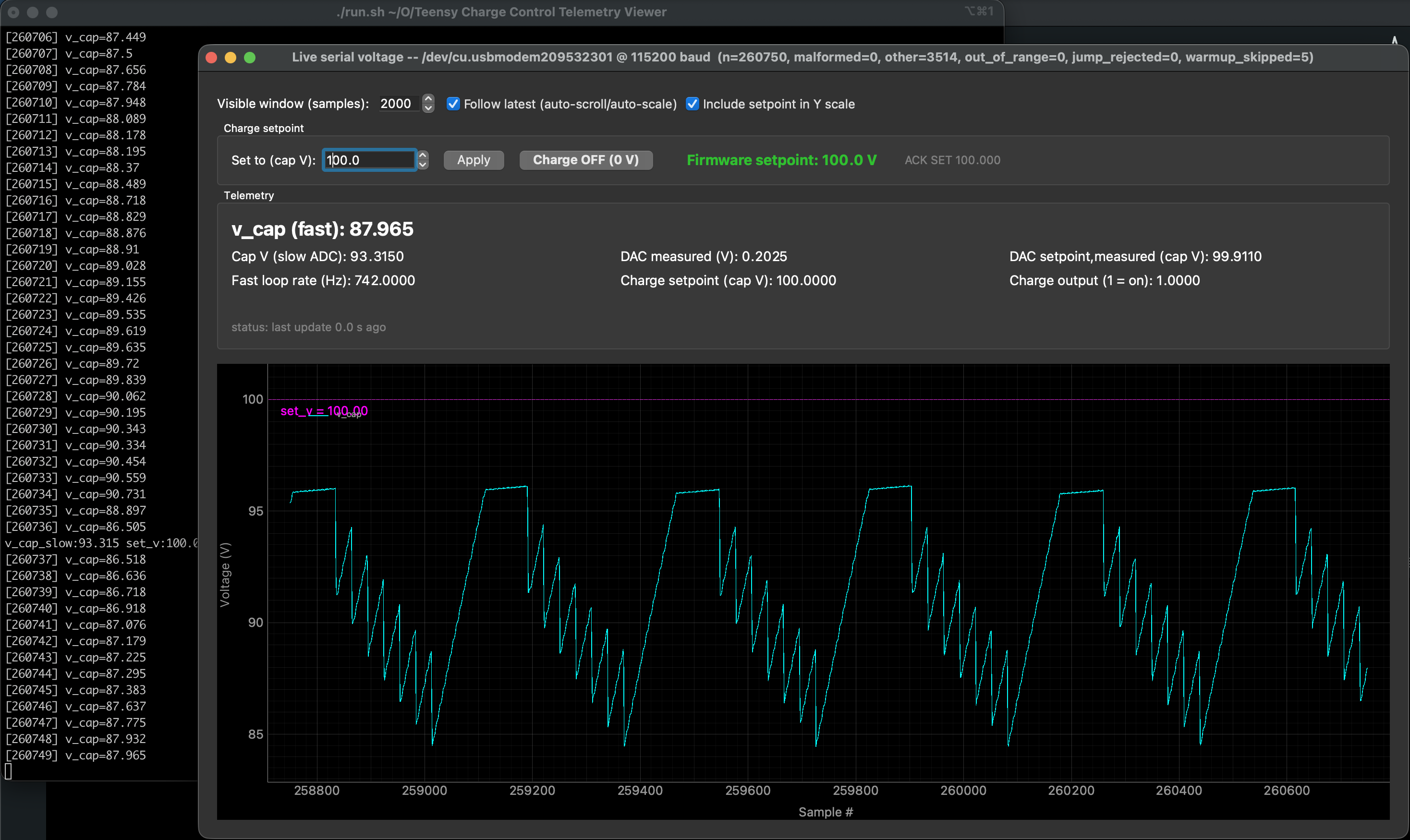
Screenshot of a python script which displays a realtime graph and telemetry from the serial output of the teensy charge-control. Also added the ability to adjust the charge-setpoint in the python window. You can see the pulse trains as the capacitor discharges, and the charge controller working as it limits the capacitor voltage at the setpoint of (close to) 100V!
Above is a screenshot of a python script which listens to voltage values sent over serial from the teensy charge controller and will display a live graph of the capacitor voltage, which is really useful for debugging as it's basically an autoscaling slow oscilliscope. The graph only shows the fast ADC's (ADS8699) calibrated capacitor voltage. It also displays other, slow-speed telemetry as numbers such as the slow ADC's calibrated capacitor voltage, slow ADC's measurement of DAC's output in both raw voltage, and the scaled/calibrated set-voltage it corresponds to (ie. I set the DAC to output a voltage which corresponds to 200V from the Micsig, I can verify that the ADC's measurement reads close enough, like 199.2V) I also added control to adjust the voltage setpoint from this python window which is useful for testing system starting from low voltage to be safe. I think there may be something with the comparator which is causing the cutoff to be slightly below the setpoint; in the screenshot you can see it cutting at ~95V instead of 100V. More calibrations....
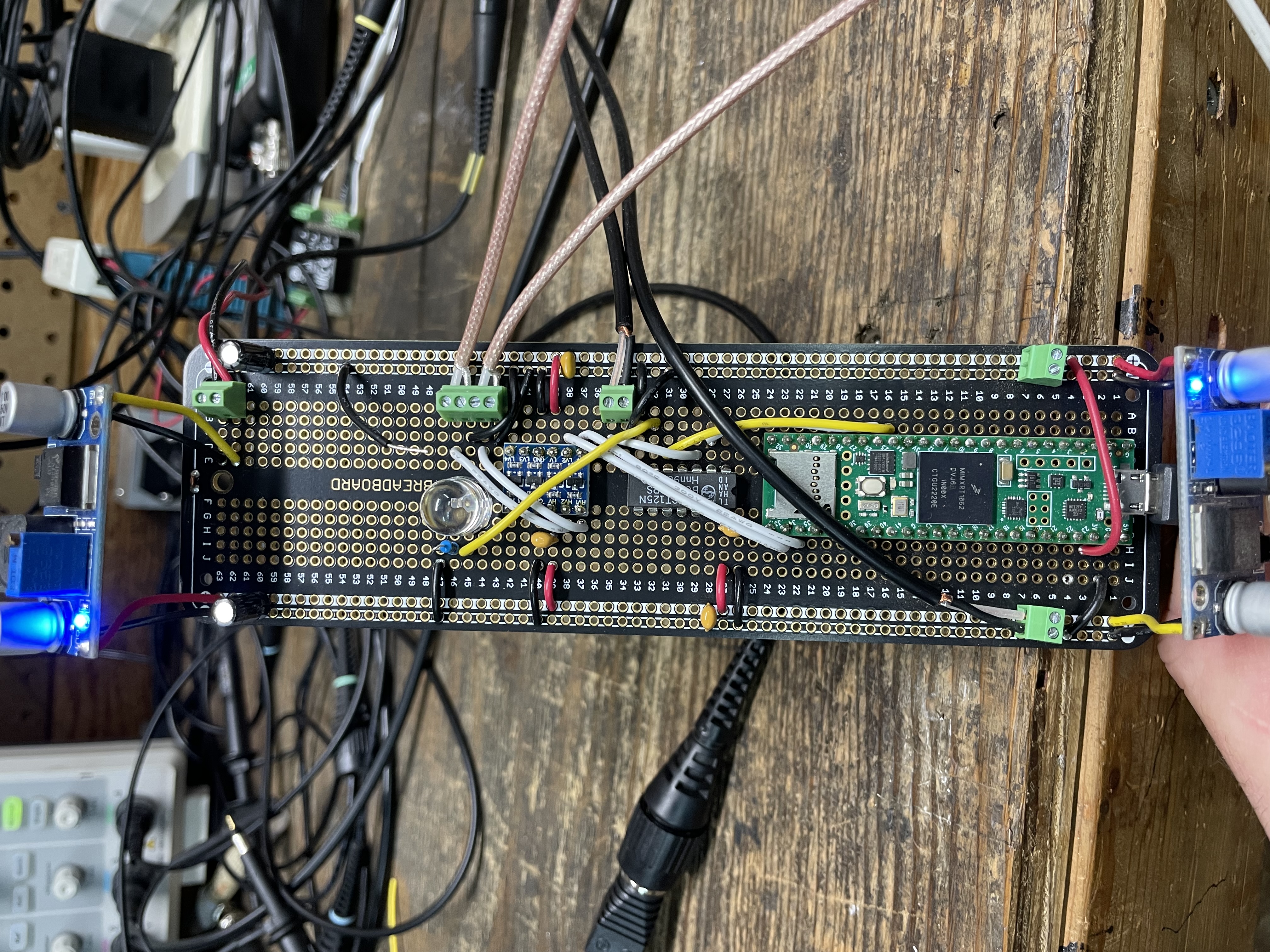
Pulse Driver Board with added inputs for RX signals from fiber-optic interface board, level-shifter and fault LED
I've made some additions to the pulse-driver control circuit as well; for a while I was just sending pulses from the teensy to the fiber-optic transmitters to fire the IGBT switches, and not reading the signal received from the other fiber line which acknowledges the driver received each pulse, and can indicate faults like a short-circuit. I wired up the fiber RX lines, ran them through a level shifter to 3.3v for the teensy to read and the teensy is now checking that each pulse was ack'd by each gate-driver, and can turn on the big-red fault LED if something's wrong. NOTE: Big-Red Fault LED will blink if the teensy detects a warning; like a an ack pulse was slightly off, or short/long. The LED will latch on if it detects a fault such as a short-circuit. It also prints this data + occasional status out over serial. The teensy code has the ability to control a safety relay to shut off main power to the system if a fault is detected, but I don't have that safety mechanical relay wired in yet, so for now, it just keeps going.
While I've built coils similar to what other systems use, I have difficulty understanding how fields from multiple coils interract/interfere to create focused peaks. I've asked Claude to build some tools to help visualise magnetic field strength in a 3-d map of various types of coils here Coil_Field_Simulator_Scripts. The simulations show for instance what happens to the field when you reverse current of one of the two figure-8 windings, or have the two coils overlap. I'm hoping that I can gather data with the Coil-Field Measurement System mentioned below, to confirm what these simulations show. I know that TMS companies construct special coils for studies called "sham-coils" which are meant to make the same sound, but the windings are wired such that the two halves of the figure-8 cancel out. These coils are used for TMS efficacy studies to give someone placebo treatment.
I've begun the coil-measurement system! at the moment I only have the data-acquisition side built and working which is in Coil-Field_Measurement_DAQ, and will have to integrate this with a 3-axis machine to move a probe around the coil to take measurements. As much as I wanted to use a high-speed ADC and teensy to measure pulses, it would have been alot of work to read and buffer 1M samples/s.... So I decided to use a faster USB oscilliscope instead; DreamSourceLab DSCope and had Claude write some python scripts which access it via the sigrok library, and visualize the results of the measurements it takes. Note; the scope I have which this code is built to interface with is a DSCope B20.
| Qty | Value | Footprint | References |
|---|---|---|---|
| 8 | 1M | Resistor_SMD:R_2512_6332Metric_Pad1.40x3.35mm_HandSolder | R15, R16, R17, R18, R19, R20, R21, R22 |
| 3 | Non-Isolated DC-DC Converter | Converter_DCDC:Converter_DCDC_Murata_OKI-78SR_Horizontal | U2, U8, U9 |
| 2 | 10K | Resistor_SMD:R_1206_3216Metric_Pad1.30x1.75mm_HandSolder | R7, R8 |
| 2 | C_0603 | Capacitor_SMD:C_0603_1608Metric | C1, C2 |
| 2 | Isolated DC-DC Converter | Converter_DCDC:Converter_DCDC_Artesyn_ATA_SMD | U1, U13 |
| 2 | R_0603_1608Metric_Pad0.98x0.95mm_HandSolder | Resistor_SMD:R_0603_1608Metric_Pad0.98x0.95mm_HandSolder | R1, R2 |
| 1 | 10000p | Capacitor_SMD:C_0603_1608Metric | C28 |
| 1 | AD5683RARMZ | Package_SO:MSOP-10-1EP_3x3mm_P0.5mm_EP1.68x1.88mm | DAC |
| 1 | AD5693RxRM | AD5683RARMZ:AD5683RARMZ | U4 |
| 1 | ADS1115IDGS | Package_SO:TSSOP-10_3x3mm_P0.5mm | U12 |
| 1 | ADS8699IPWR | Package_SO:TSSOP-16_4.4x5mm_P0.65mm | ADC |
| 1 | IRG4PF50W | Package_TO_SOT_THT:TO-247-3_Vertical | Q3 |
| 1 | LM2931-5.0_SO8 | Package_SO:SOIC-8_3.9x4.9mm_P1.27mm | U11 |
| 1 | LM293DR | Package_SO:SOIC-8_5.3x5.3mm_P1.27mm | Comparator |
| 1 | MCP1415 | Package_TO_SOT_SMD:SOT-23-5 | U10 |
The 28 most common of 42 parts.
open-ephys/ephys-test-board
General purpose, automated electrophysiology test board


Bojtronic/TFG
Trabajo final de graduación para el grado de licenciatura en ingeniería en computadores


Jsnchg/Heavy-Operations-UI-Industry-System-B-C-eVTOL

42 parts, built around the IRG4PF50WPBF, ADS1115IDGS, MCP1415-E/OT and AD5683RARMZ. The full list of its parts is on this page, with links to each part's symbol and footprint where PCBKit's library has them.
From the zmcginty/OpenTMS repository on GitHub, at the commit this page was made from: the board is Kicad System Schematic/TMS_IGBT_And_Gate_Drive/TMS_IGBT_And_Gate_Drive.kicad_pcb and its schematic Kicad System Schematic/TMS_IGBT_And_Gate_Drive/TMS_Charge_Controller/TMS_Charge_Controller.kicad_sch. PCBKit opens the board in the browser, with nothing to install.
Its repository states no licence, so its author keeps all rights: ask zmcginty before reusing the design.