
2 layers
 zinziroge/split_keyboard
split_keyboard
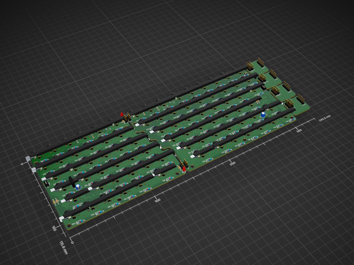
Skb i2c lefthand is an open-source printed circuit board by zinziroge, from the zinziroge/split_keyboard repository on GitHub, published under the MIT licence. It is a 2-layer board of 330.5 × 115.6 mm with 231 parts on 209 nets, routed with 1,520 tracks and 229 vias.
It is built around the PCA9515AD. Its parts include 85 diodes, 85 switches, 10 connectors, 6 resistors and 4 ICs. It belongs with the keyboards and input boards of this library.
split_keyboard.
| Qty | Value | Footprint | References |
|---|---|---|---|
| 83 | 1N4148 | Diode_THT:D_DO-35_SOD27_P7.62mm_Horizontal | D1, D2, D10, D11, D12, D13, D14, D15, D16, D17, D18, D19, D20, D21, D22, D23 +67 |
| 83 | SW_PUSH | keyboard_parts:Kailh_MX_Socket | SW1, SW2, SW10, SW11, SW12, SW13, SW14, SW15, SW16, SW17, SW18, SW19, SW20, SW21, SW22, SW23 +67 |
| 11 | Val** | kbd:HOLE | Ref**, Ref**, Ref**, Ref**, Ref**, Ref**, Ref**, Ref**, Ref**, Ref**, Ref** |
| 10 | Conn_01x04_Male | Connector_PinHeader_2.54mm:PinHeader_1x04_P2.54mm_Vertical | J_PIKO_4E1, J_PIKO_4E2, J_PIKO_4E3, J_PIKO_4E4, J_PIKO1, J_PIKO2, J_PIKO3, J_PIKO4, J3_PIKO_R1, J5 |
| 6 | Conn_01x05_Male | Connector_PinHeader_2.54mm:PinHeader_1x05_P2.54mm_Vertical | J_PIKO_1, J_PIKO_2, J_PIKO_3, J_PIKO_5, J2, J3_PIKO_L1 |
| 6 | R | Resistor_THT:R_Axial_DIN0204_L3.6mm_D1.6mm_P7.62mm_Horizontal | R1, R2, R3, R4, R5, R6 |
| 4 | Conn_01x03 | Connector_PinHeader_2.54mm:PinHeader_1x03_P2.54mm_Vertical | J7, J8, J9, J10 |
| 3 | I2C_A2 | Jumper:SolderJumper-3_P1.3mm_Open_RoundedPad1.0x1.5mm_NumberLabels | JP_A3, JP_SCL1, JP_SDA1 |
| 2 | CP | Capacitor_THT:CP_Radial_D5.0mm_P2.50mm | C1, C2 |
| 2 | Conn_01x04_Male | Connector_PinSocket_2.00mm:PinSocket_1x04_P2.00mm_Vertical | J3, J4_GROVE1 |
| 2 | I2C_EN | Jumper:SolderJumper-2_P1.3mm_Open_RoundedPad1.0x1.5mm | JP_I2C_EN1, JP4 |
| 2 | LED | LED_THT:LED_D3.0mm | D84, D85 |
| 2 | MCP23017_SO | Package_SO:SOIC-28W_7.5x17.9mm_P1.27mm | U1, U3 |
| 2 | MJ-4PP-9 | kbd:MJ-4PP-9_1side | J1, J2_TRRS1 |
| 2 | PCA9515AD | Package_SO:SOP-8_3.9x4.9mm_P1.27mm | U2, U4 |
| 2 | SW_DIP_x01 | Button_Switch_THT:SW_DIP_SPSTx01_Slide_6.7x4.1mm_W7.62mm_P2.54mm_LowProfile | SW84, SW85 |
| 1 | Conn_01x04 | Connector_PinSocket_2.54mm:PinSocket_1x04_P2.54mm_Vertical | J6 |
| 1 | I2C_A0 | Jumper:SolderJumper-3_P1.3mm_Open_RoundedPad1.0x1.5mm_NumberLabels | JP_A1 |
| 1 | I2C_A0 | Jumper:SolderJumper-3_P1.3mm_Open_RoundedPad1.0x1.5mm | JP1 |
| 1 | I2C_A1 | Jumper:SolderJumper-3_P1.3mm_Open_RoundedPad1.0x1.5mm_NumberLabels | JP_A2 |
| 1 | I2C_A1 | Jumper:SolderJumper-3_P1.3mm_Open_RoundedPad1.0x1.5mm | JP2 |
| 1 | I2C_A2 | Jumper:SolderJumper-3_P1.3mm_Open_RoundedPad1.0x1.5mm | JP3 |
| 1 | I2C_SCL | Jumper:SolderJumper-3_P1.3mm_Open_RoundedPad1.0x1.5mm | JP5 |
| 1 | I2C_SDA | Jumper:SolderJumper-3_P1.3mm_Open_RoundedPad1.0x1.5mm | JP6 |
| 1 | Power | Connector_PinSocket_2.54mm:PinSocket_1x04_P2.54mm_Vertical | J4 |


Envious-Data/Env-KB
A custom mechanical keyboard inspired by the CFTKB Mysterium utilizing the Raspberry Pi Pico

UzixLS/zxuno1010-board
10x10cm PCB variant of ZX-UNO project for G738/G706 enclosure

OpenModbus/OM-64DO
A compact industrial-grade 64-channel Modbus RTU output module.

Duckle29/pulsr
A simple tiny PCB for handling the high peak currents of periodically firing a solenoid


It measures 330.5 × 115.6 mm and has 2 copper layers, 1.6 mm thick.
231 parts, built around the PCA9515AD. The full list of its parts is on this page, with links to each part's symbol and footprint where PCBKit's library has them.
From the zinziroge/split_keyboard repository on GitHub, at the commit this page was made from: the board is kicad/skb_i2c_twohand/skb_i2c_lefthand.kicad_pcb. PCBKit opens the board in the browser, with nothing to install.
Its repository publishes it under the MIT licence: you may reuse it on that licence's terms (keep the author's notice, and for a copyleft licence share your changes alike).